Note: Descriptions are shown in the official language in which they were submitted.
` 13239 ~ 3
OADB~D MICROSTRIP TO COI'LANAR
W~EGUIDE T~NSI~ION l~lr
ANISOTROlPIC ETClE3[ING
OF GALI,IlLJM ~SENIDI~
s
Field of the InYentiort
This invention pertains to a method and apparatus for
connecting dissimilar miniature electronic transmission lines, more
particularly or broadbandl connection of a microstrip to a coplanar
10 waveguide.
~ackground of the Inve~tion
Electronic devic~s for ultra-high frequen~y microwave signals
(>10 GHz) are difficult to design because interconnections have
15 unintentional capacitance and inductances, causing undesirable side
effects. Dissirnilar families of microwave electronic devices, desirable
approaches in themselves, become an extremcly dificult problem to
put together without causing parasitic distortions of the signal.
At microwave frequencies there are no simple interconnects to
20 be used in integrated circuits. Simple low frequenc3~ interconnects
show dispersion, attenuation, and phase shift at microwave frequencies
and therefore have to be designed and treated as transmission lines.
There are a number of popular transmission line geometries available
for microwave circuits. The simplest and most widely used structure
25 is known as a microstrip. (see
T.C. Edwards, Foundations for Microstrip Circuit Design, John Wiley
and Sons, 1981.) A microstrip consists of a metal strip of contrvlled
willth on the surface of the semiconductor or ceramic substrate. The
~r 87--~1
-~ ~ 323913
other side oE the substrate is completely metalized and forms the
microstrip ground plane. Another transmission me~!ium used in
microwave circuits is known as coplanar waveguide (CPW).
The difference between Cl'W and microstrip is
5 that CPW has all the conductors including the ground plane on Ihe
sarne side of the substrate ad~ling the a(lvantage of easier access to
ground.
Microstrip and CPW are generally not combined on the same
monolithic circuit. But it is desirable to be able to connect CPW
10 circuits to microstrip circuits in order to forrn larger subsystems.
Obi?ects o~ the Invention
An object of the invention is to provide a broadband transition
for microstrip to coplanar wave~uide in a GaAs monolithic circuit,
It is a further object of the invention to provide such a
ttansition without the use of via holes in the GaAs substrate.
Summa~y of ~the ln~ention
These objects of the invention and other objects, features an~l
20 ~dvantages to become apparent as the specification progresses are
accompl~shed by the invesltion according to which, briefly stated, a
procedure is described for making a broadband transition between a
microstrip line and a coplanar waveguide on a thick GaAs substrate.
In order to form a broadband transition between two transmission
25 media, it is necessary to minimize the parasitic reactances associated
with the geo~netr;cal discontinuities of the transition. In order to
achieve this for a transition between microstrip and coplanar
waveguide, we keep the center conductors vertically at the same level
connectetl by a tapered section. The ground planes ~herefore call not
87 ~1
., ' :~ .
, ' ., ~ ~ :, ,
: ?
:
: ` ., .
~.3 ,c~3~3 13
be at the same vertical level and need to be connected by a low
inductance path. This is achieved by a metalized sloped wall formed
by anisotropic etching of GaAs. In silicon monolithic circuits, the need
for the extra bandwidth that this transition offers does not exist,
S because silicon integrated circuits are not yet fast enough. The
advantage of GaAs circuits is their added speed. It is at these high
frequencies (greater than about 10 GHz) where (i~aAs integrated
circuits operate that the extra bandwidth becomes necessary.
These and filrther constructional ar~d operational characteristics
of the inven~on will be more evident from the detailed description
given hereina~ter with reference to the figures of the accompanying
drawings which illustrate one preferred embodirnent and alternatives
by way of non-limitLng examples.
BrieDescription of the Drawin~s
FIG. 1 shows a schematic of a coplanar waveguide.
FIG. 2 shows a schematic of microstrip.
FIG. 3 is a schematic of the planar approach for coplanar
waveguide to microstrip transitions.
FIG. 4 is a schematic of the coplanar ground planes approach
to coplanar waveguide to micros~ip transitions.
FIG. 5 is a schematic of the coplanar center conductors
approach to coplanar waveguide to rnicrostrip transitions.
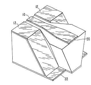
FIG. 6 is a schematic perspective view of the tapered microstrip
to coplanar waveguide transition on ceramic.
FIG. 7 is a detailed layout of the tapered microstrip to coplanar
waveguide transition on ceramic.
FIG. 8 is a schematic of a microstrip to coplanar waveguide
transition on GaAs USillg anisotropic etching according to the
87-4
`"
:
ll 323~
invention.
FlG. 9 is a simplified top view of top surface of t~le ~levice of
FIG.8.
FIG. 10 is diagram of an array of the devices of FIG. 11 on
5 a semîconductor substrate.
FIG. 11 is a diagram of the same array as in FIG. 10 with the
areas to be etclled shown in shading.
Fig. 12 is a section of the etch along the section line 12-12 on
FIG. 11.
FIG. 13 is a section of the etch along the section line 13-13 on
F~G. 11.
FI~. 14 shows the array of FIG. 11 highlighting the pattern of
met~ zation imposed on the top surface after etching in shading.
FIG. 15 shows in dotted lines the die separation of the array of
FIG. 1:1 into individual devices.
FIG. 16 shows a sample mask used for the substrate etching of
the transitiQn device .
FIG. 17 shows a sample mask used for the top surface
nnetalization oE the transition device.
FIG. 18 is a graph of measurements of insertion loss and return
loss measured for two back to back transitions.
Lexi~olll
-
~e portion of the elestromagnetic spectrum between UHF and
infrared is normally referred ~o as microwaves. It corresponds to the
frequency range between 1 GHz and 300 GHz.
A transmission line is a structure used to guide the
electromagnetic wave. Microstrip and coplanar wavegui(le are
examples of transmission lines.
~.
87-41
:
: ~ .
,
" ~3~3~13
A transmission line is normally used in a regime where it can
carry only one propagation mode. Other propagation modes
unintentionally excited are referred to as extraneous modes. (See:
Ramo et al., Fields and Waves in Communication Electronics, John
S Wiley and Sons, 1967.)
Glossa~
The following is a glossa~y of elements and structural members
as referenced and employed in the present invention.
lû coplanar waveguide
12 ground plane of the coplanar waveguide
14 wafer
- 20 micros~rip
22 ground plane of the microstrip
30 via hole
Deser~ption of the Preferred Emlbodimellts
Refening now to the drawings wherein reference numerals are
used to designate parts throughout the various figures thereof, tllere
20 is shown in FIG. 1 a schematic of a coplanar waveguide 1(), in the
prior art. The ground plane 12, a thin film of metal, on this stn~cture
is on the top side of the wafer.
The wafer 14 material is GaAs or other suitable semiconductor
material on which most microwave integrated circuits are fabricated.
25 The thickness of this wafer, h9 in the case of coplanar waveguide is
usually kept at 400 microns or higher for ease in handling. This
dimension is not critical for propagation characteristics of CPW. The
characteristic ;mpedance of the transmission line is mainly determined
by the dimensions W and G. In the case of microstrip, wafer
87 1]
.
323~13
thickness h is a critical dimension. This dimension together with the
width of top conductor W, determines the characteristic impedance of
the transmission line. In this case substrate thickness is usually on the
order of 100 microns. The thin substrate allows for via holes to be
5 etched in the wa~r to connect top surface components to bottom
surface ground.
A microstrip 20, as shown in FIG. 2, has its ground p]ane 22,
a thin film of metal, on the bottom side of the wafer, as shown in
FIG. 2. One side of wafer is comp3ete3y metalized. This is the
10 bottom side of the wafer. r~he meta;ization is used as the ground
plane for the micro~trip line. The role of a transition between these
two dissimilar transmission lines is to elec~rically connect the ground
planes of ~he two lines and also the center conductor of the coplanar
waveguide to the top conductor of the microstrip.
At ~equencies below 10 GHz~ some of the approaches taken
are shown in FIGS. 3-5. The planar alpproach, as shown in FIS~. 3, is
inherent~y narrow band. Such narrow band transitions can not be used
in conjuDction with wideband components such as distributed
amplifiers. Also, narrow band interconnections cause signal distortion
in fast digital circuits. The non-planar approaches, as shown in FIGS.
~5, use bond wires ~small sections of gold wire) to connect either the
ground planes or the center conductors. At higher ~equencies, the
bond wire inductance can lead to the excitation of e~traneous modes
on the coplanar line. ~See Riaziat et al., Coplanar Waveguides for
MMICs, Microwave Journal, June 1987, pp. 125-131; Riaziat et al.,
Single Mode Operation of Coplanar Waveguides, Electronics Letters,
Vol. 23, No. 24, Nov. 1987, pp. 1281-12~3.~ Via holes can be used
instead of bond wires to reduce the inductance. However, since one
of the advantages of using coplanar waveguides is the possibility of
avoiding via holes in $he GaAs process, this is not an attractive
87-1 1 ;
: ` ~
` ~ , ,
.
~.
3L323~1~
solution. The via hole process for G~As monolithic circuits ;s an
expensive and yield limiting step. Via holes in ceramic substrates are
more practical since they are drilled using lasers or ultrasound, and
their process is separate from that of the monolithic circuit.
5 Broadband transitions can be designed using via holes in ceramic. An
example of this device is shown in FIGS. 6-7. However, since the
inductance of a via hole 30 is in general higher than that of the sloped
surface used in the invention, these transitions are not as broadband.
The approach according to the invention makes use of an
10 anisotropic etching of the GaAs substrate to achieve a slope~ surface.
This sloped surface, when metalized, makes a low inductance
cormection between the two ground planes, as shown in FI~;. 8. To
unders~and the fabrication method of the device of FIG. 8, Figs. 9-11,
1~15 should be studied in sequence. FIG. 9 is a simplified schematic
15 top view of top surface of ~he device of FI&. 8. FIG. 10 shows the
layout of an array of the devices of FIG. 9 for batch fabrication on a
semiconductor substrate. FIG. 11 shows the etched area shaded. The
etch must continue all the way through the serniconductor subtrate.
Any of the etches used for mesa and gate recess definiation for GaAs
20 F~T's will do if GaAs is the chosen material. Because of the slowness
of the [ii1~ surface lo virtually any wet etch, the wafer should be
aligned so that a "vee" will form in the vertical direction, as shown in
the section 12-12 of FIG. 11 and FIG. 12. Also, a "dovetail" will form
in the or~horgonal direstion, as shown in the section 13-13 of FIG. 11
25 and FIG. 13. The "dovetail" is not necessary for the operation of the
device of the invention. If anything, it complicates things. The angle o
shown in FIG. 12 is approximately 55~. (See: J.Electrochemical Soc.
~, p.118, 1971; J. Electrochemical Soc. 128 p. 874,1981.) The type
of etch used is dictated more by the ability of the mask (photoresist
30 etc.) used to stancl up to it for a lon~ period of time than by anything
8741
239~3
else. Even dly etching could be used, taking care that the angle ~ lies
in the 40 to 70 range. Angles less than 40 will result in an
excessively large device and greater than 60 will result in poor metal
coverage and a sudden transition from coplanar to microstrip, causing
S spurious mode generation and larger radiative losses. ~IG. 14 shows
in shading the metallation patterm superimposed on the array of FIG.
11 after the etching step. FIG. 15 shows in dotted lines how where the
array is die cut to separate individual devices either by diamond or
Iaser scnbing.
Two optical masks are used in the fabrication of the transition.
The i~rst mask, shown in FIG. 16, is used for substrate etching using
a solution of H2SO4:H2O2:H2O. ~IG. 17 shows the second ~nask used
for top su~ace metalization.
An example of the the de~ails of the photolitho~aphy steps
follows:
(1) GaAs wafer is cleaned using TCE, Acetone, and IPA.
(2) The backside of the wafer is metalized with evaporated
Ti/PtlAu, at 2SO/1SO/26~8L
(3) The backside of the wafer is coated with AZ; 1350J
photoresist at 3000 P~Ph~[ and baked at 80C for 30 minutes.
(4) The front surface is liquid pnmed using HMDS at 6000
RPM, then coated with photoresist according to step ~3~.
(S) Mask No. 1 as shown in FIG. 16 is used to e~pose the
front side of the wafer with W400 light at 20 mW/cm2 for 10 seconds.
The long side of the rectarlgles shoulcl be aligned parallel to the [011]
direction on the wafer.
(6) The resist is developed in AZ 351 developer (5:1), for
30 seconds, and baked at 100C for one hour.
(7) The wafer is ashed at 100W for one minute.
87~1
'
,
.
:L3239 ~?J
(8) GaAs is etched in a 1:8:1 solution of H~04:H202:H20
for 35 minutes (etch rate: 10 ~m/min at room temperature).
(9) The photoresist is stripped by Acetone.
(10) Front side of the wafer is coated with AZ 1350J
S photoresist at 3000 RPM, and baked at 80~C for 30 minutes.
(11) Mask 2 as shown in FIG. 17 is exposed for 13 seconds
and developed according to step 6.
(12~ Layers of TUPt/Au are evaporated on the front surace
with thicknesses of 150/50/30~
(13) Steps 10 and 11 are repeated.
(14) The wafer is baked at 1~C for 30 minutes.
~153 2 microns of Au is electroplated on the surface.
(16) Photoresis~ and extra metal is removed by a lift-off
process in ~But~rol Ac~one.
Measured insertion loss and re~urn loss for two back to back
trarlsitions is shown in FI~:;. 18. ~s can be seen, 15d~ return loss is
achieved with a band width of 23 ~:;Hz. This large bandwidth has not
been obtained by any of the other $ransition schemes mentioned.
This invention is not lirnited to the preferred embodiment and
alternatives heretofore describsd, to which variations and
improvements ma3r be made, i~cluding mechanicaDy and electrically
equivalent modifications to component parts, without departing form
the scope of protection of the present patent and true spirit of the
invention, the characteristics of which are summar~zed in the fo]lowing
claims.
87-4 1
. .
. .