Note: Descriptions are shown in the official language in which they were submitted.
~323~21
~5
This inY~ntion rola~es to opti~al component~ for use with
optic~l fi~r~ ~nd osh~r op~ic~l w~eguid~s, ~nd t~ methods of
5 m~nufacturing sucbl compo~eIIts. I~ pnrticular9 th~ugh not
excl~sivel~r~ thi~ inv~ntion ~elat~ to outo-elec~ronic ~omponent~
for eransmitting, ~oiYin~ or other~i~ proces~;ng opti~l signal~,
arld, their manuf~t~
,
T~ae dimension3 of th~ ~cti~e, or ll~ht ~mitting, ~e~ ~f ll~h~
~ources ~such a~ s~ conducto~ la~ and ll$ht emlttlllg ~od~)
u~cd in opti~al flbse communications sys~em~ a~o typically of th~
o~der of ~ f9w ,Um. In a 8~n~le n~odo op~ical i~b~c suitabl~ for
us~ in ~lle 1.3,um ~nd 1.~11nn w~Yele~lgth ~ions th~ ~ore is
~bout 5-10~m in diamo~er.~ e~nt optic~1 eoupl~ng betwe~n
the 1b~ ~nd tho light sourco ~equ~r~s th~t their al~nment b~
a~cura~ to within ~ few ,u~ (o~ 1~3s), both ~ran~v~s~ly and
axially.
2 0 Tho dltn~n~lon3 of the a~ti~o ~e~ of photo~dete~tors are
usually lar~er, of th~ order of 5~-lOO~lm and tho ali~nnlent
tolorances betweell the ~ib~ ~nd thç dete~to~ an~ally moro
~elaxed. ~owever, in th~ ~a~e of an optical t~:aYelli~g WAYQ
amplifi~r, for ~x~mplo, th~ l~ght sen~ reçoiving area o~ ~he
2S devl~ of th~ ~ne dlmen~ions ~s th~ act~vo are~ o~ a las~.
'~
...... .. . . . ..... ,.. ", ....... ~.. .......... .......... . ................... . . ....... .... .. ....... . . . ', . '
~ ~ ,
~" :
; .
~.
.3 2 ~, ~ S~3J ~
.
Th~ n~ for ~on~tently high a~cura~y of optic~l
alignm~nt~ fo~ms o~o of tho n~a~o~ p~oblem~ whlch needa to b~
overco~o lf op~iaal d~ cG6 aro to be manufactu~od ~n la~e
vol~mes, Lar~o Yoll~lme tm~nuf~tllre i8~ of oollrse, o~sential to
5 reducin~ tho ~ost of optic~l fib~ ~oln~unic~on~ syst~ms.
P~rman~ntIy attachin~ a fibro "pi~tail" to the dovi~ is ~no oil the
wid~ly ~dopted solutions. H~re, the critical alignment betw~en
the fi~rc and thc devi~e is made dur~ng mallu~a~ture. To connect
10 the d~Yice to an optical fib~ ~ansmlss~o~ lin~, a ~lati~ly ea~ily
ali~ned fib~e-to-fibr~ . spli~o is formod betwee3l Sho pi~tail ~nd
tho t~ansmi~sion ibre. U~e of a spliced conneati~n i~ readily
acceptablo only in applio~ions wher~ tho coImoc~ion betwoer~ tho
optical devico and the tran~mi~siorl fibre needs r~ely i~ ov~r to
15 ~e bsoken ~r ~e-made.
,
GB PRtent 155~0~3 (VImp~ov~ment~ in or relating to
. dioloat~iG optii~al wav~uid~ ~ouplings", T}~ P~st ~)ffio~ disclo~a
an opto-cle~on~o ~ompon~nt in ~vhlch t~ op~-oleatron;~ d~vlc~
2 O ~8 hOgSI~d il~ An .optic3ill fibre conn~tor. Th~ opt~-olectroni~
d?vice may be located in ei~hos tho malo c~r tho fom~lo p~rt of
tho connector. This a~an~msnt of ~n optical dsvic~ mounted in
~rl optical fibre ~onneoto~ ometimes re~er~cd to a~ a
"connectorisQ~ deYic~
26
................ ... .... ...... ....... .. . ... .... . ....... .. .. . .. .. . . . .. . . . .. .
1323~2~
use of a connector-mounted device permits easy
and repeated connection and disconnecti~n between the fihre
and the device and is potentially fairly cheap to
manufacture. Ensuring adequate optical alignment between
the fibre and the device does, however, present some
difficulties.
The present invention aims to provide a method of
manufacturing optical components, which will more reliably
yield adequately accurate optical alignment. The present
invention also aims to provide a connector-mounted optical
component made by that method.
According to the present invention, a method of
making an optical component comprises inserting a pre-
assembl0d device carrier, comprising an optical componenk
mounted on a support structure, into a mould, filling the
mould with light and/or thermally curable material,
optically aligning the device assembly and, on achieving
alignment, at least partially curing the material to form
an alignment shell about the device carrier.
Any partial curing of the material must be
sufficient to ensure adequate rigidity to avoid relati~e
movement of the parts until full curing has taken place.
Full curing preferably takes place at elevated
temperature.
i ~
.
~ .
. .
:,
:
~ : ,
~323
.. ,
A~ording to anoth~r a6p~t of th~ present in~ention, aln
optlcal compotlent compris~s ~ pre~assembled devi~e ~arrior
~omp~ising a 31~pport ~tru~ture and an opti~ omponent
m~unted the~on, ~nd further comprises an a~i~nment shell
5 about th~ ~v~ caxrl~r form~d of li~ht and/or theTmally cured
matGrial.
Prefe~Ably, th~ optlc~l component i~ ~n opto-olect~onic
compon~t ~apab~ oP conv~rdn~ ht into an elec~ ig~ r
10 vi~e v~r~a.
Th~ p~e~ nv~ntlon ~vlll now b~ ~scribod fur~ho~ by
way o~ ex~mpto only, an~ witlh f~r~nc~ to tho acaompanying
drawin~, of whiah:7
1~ , .
~i~ure~ 1~ to lf a~ sch~matic illustrations o~ v~iou~ sta~e~
in tho manufactu~o accordin~ to ~he p~e~ent inv~ntion of an
opto-elGc~ronic eornponent;
.20 ~igur~ 2 is ~ s~hem~tic BO~S~Ollal ~tiew of a~ opto~ onic
componont mado ac~o~ding to thc m~th~d illu$~te~ in
~ig~e l; and
Figure 3 i~ a schemati~ ~ect~onal ~iew of a modifi~d ~pto-
2 5 electronic componon~.
.. ' ; ' . . : . ' '
,- : , .
i, ~ '
~32~
.. .
~ efor~in ~o~ ~l~o to the d~awln~s, Fi~ sh~w~ a pf~-
ass~lnbled ca:rrier 1 for an opto-elec~onia doYic~ 13, Tho ~arrie~
1 comp~isa~9 ~ tubular ~er member 11 ~f con~u~tlve material,
having mounted on a flnt mounting ~u~face at a st3pped end ~2
5 thereo~ ~n opto~olect~onlc device 13. Secured ~y adhosi~ ln
14 to the opto~ tronic devlc~ 13 and tll~ 3tepped end 1~ of the
eamer mern~er 11, i~ ~ spherical ~oll~n~atin~ o~ P~cus3ing lerls lS.
~lectri~t collne~ions t~ the opto-el$ctroni¢ d~vico 13 a~e
pr~Yi~ed by th~ tubulal me~3b~r 11 i~lf9 and by a t~mlnal 1
10 of ~ wiro 17 (see Pi~ure ~) lnsulated ~rom, and o~tendi~ h~
len~th of, th~ tubul~ m~mb~r I 1.
l~igur~ 1 b show~ a mould 2 in wh~ to form an alignment
shell around ~he c~e~ 1 of ~i~ure la. The mould ~ompri~es
16 ~wo ~xl~lly ali~led cyli~ al ~lee~ portions 21 and 22,
~epa:rat~d by an intermediate w~ . Thc ~leeve portion 21 is
of an inter~al diameter l~ger tha~ th~ maximum transYer~e
dlmension of tho c~ r l; ~he ~leev~ po~tiorl 22 plio~i~e~ a push
fit a~out all optic~l fibr~ connocto~ ferrule ~4 ~nclosing All
2 0 opti~l fibre 25 and ~nding flu~h wi~h tho ~ 25. The
in~ermediato wall 23 i~ ~la8 an aper~ure ~6 which l~cat~ a plu,~
~7 o~ silicone ~ubb~r o~ another ~u;t~ly re~iiient ~ate~i~l which
i3 tFan~pa~ont at the w~Yel~n~th o~ operation of the opt~-
ele~t~onic devi~e 13.
~6
, ", ,, , ,,,, .. " . ", . ........ .. .. ..... . .
:~. 3 ~
,
A~ illustrat~ y FiKu~e~ lc ~o lf, e}lo manu~t~ of . ~n
opto-elect~on~c comp~nent p~oc~ds a~ follow~:-
The p~e~a~sembl~d ~ r 1 is in~tcd fully into th~
S sleove portion ~2 of mould 2 llntil it tou~h~s and xlightly d~orm~tho plug ~7. The~eupon the mould is filled wlt~ a liquid, IJV and
th~ eurablo mat~rial as ~ch~m~ti~lly ;~dicated by ~ho funnel
2~. To b~ suitablo sho ~rial n~ust have ~oo~ e~Yironmen~al
sta~ility wh~n cured. M~tlla~ylate re~n p~oviding ~ Ina~ix ~r
1 Q finely gro~nd b~ro-sil~ate ~la~s h~s ~ecn found to be ~atisf~ctoxy
in thi~ ~esp~t.
~ G~ tho mould ls filled, t~. ç~Tricr 1 ia mov~d
transv~rBe,ly until optimum ~lignmGnt b~t~n th~ do~ 13
and tho co~e 2~ of tho op~lc~l fib~e 2S h~ ~eon a~hi~ved a~ :
m~asured by th~ unt of li~ht ~Qupled il~o o~ ~u~ of the f~br~
~5. It should be noted th~t th~ les~ nt plug ?-7 w~11 p~o~,ride
ba~ior to tho liquid mould fe~d ~hereby to aYoid contaml~tlon
of the f~ont po~l~n of tho 5urfACO of the long 15.
~ .
On reaching optimurn ali~s~flnt, the mould f~d ;s at l~ABt
pa~tly ~lr~d ~y ~lTadi~tlon with li~h~ ~rom a UV ~ou~ 31)9 ~s
~ohematically s~ow~ in ~i~ure le This UV. c~ring p~oces~ ~ust
~ult in sdequate dimens10nal stability to ~llow removal of the
5 complet~ ;I component 4 ~rom the m~ul~ 2 without ~ rse~y
affect~ the positior~in~ of the carr~er i ~i~hin the nlolllded shell
' , ' '~,~ ,' , : '
.~
~32392 ~
31. Ins~ead of irradiating the resin from the end of the
mould, a transparent mould irradiated from all directions
could be used, for example.
If required by the material properties, the
curing process can be completed at elevated temperatures as
indicated by Figure lf.. Suitable elevated curing
temperatures are typically 80C to 150C.
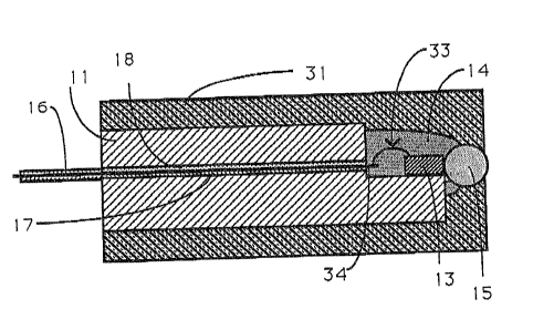
Figure 2 shows a schematic length-wise section
through a completed opto-electronic componellt. In addition
to the features of the carrier already described with
referance to Figure la, there is shown the central
conductor 17 leading, within an insulating sleeve 18, from
the terminal 16 to a bonding pad 3~. A bond wire 33 is
attached to the bonding pad 34 at one end, and to a top
contact of the device 13 at its other end.
The shell 31 provides a highly concentric
alignment surface around the component which thus can
provide a male portion of an optical ~ibre connector, for
example.
Figure 3 shows a schematic length-wise section
through a modified form of the component of Figure ~.
Using a resin matrix for ground boro-silicate glass
provides an external surface to the shell which is of
excellent thermal and mechanical stability; however, the
glass particles in the material or the matrix
.~.
' :
''
. .
:,
1 3 ~ J ~
mat~rial it~lf may provG to b~ too nbra~iv~ in ~e~tain
applications. To ~-~er~mo this, tho shell may ~o ~nclos~d in a
thin sle~ 35 of nnaterial mors closely m~t~h~d ln hardn~ to
the material ~ the ~ocke~ in~o which the con~po~onS ~ to b~
5 in~erted.
I .
,
,
... ..... .. . ... .~.. , ............ ...... ..... .. . __.. . .. ... .. .... ,, ,.. , , ....... ........ .... ...... , ., .. _, .,.. .
. ~ . ; .... ._
. -
.