Note: Descriptions are shown in the official language in which they were submitted.
132~7
MICROPROCESSOR HAVING EXTE~L
CONTROL 8TORE
Field of the Invention
This invention relates generally to digital data `
processors and, in particular, relates to an integrated ` -
circuit microprocessor having a number of new and
useful features~
Bac~ground of the InventioA
IntegratQd circuit microproce~sors are widely used for
a variety of digital data processing applications. In
general, most coAventioAal microprocessors comprise an "~
arithmetic~logic unit (ALU), a plurality of rQgistQrs,
. ~ ~
and a m~mory address and data buæ which may or may not
be drlv~n e~ternally from the chip. Program
instruction~ read from th memory are decoded into one
or more microinstructions, the microinstructions
opQrating to control the internal logic of the
microprocessor to accomplish a predefined action as
spQcified b~ the instruction~ For example, an ADD
.
1324~7
instruction is ~ypically decoded into a plurality of
microinstructions which perform the task of accessing
the data to be added, directing the data into the ALU `~
and storing the result of the addition. In
conventional microprocessors these microinstru~tions
are stored internally within a control store which is -- -
typically a read only memory which is integrated within
the microprocessor circuitry. This creates a problem
in that the control store is normally inaccessible to -
devices outside of the microprocessor, making the
reading and/or modification of the microinstructions ``
within the control store by external devices difficult - :
or impossible. `
"'^-"'"`'`"`'.
One such external device may be a coprocessor, such as
a floating point arithmetic acceleration unit. Such
acceleration units typically work in con~unction with `
the~microprocessor and pro~ide extended mathematical
capability in those applicationæ where such extended
cap~bility i8 required. As can be appreciated, the
degree of coupling between the microprocessor and the ` `
coprocessor is an importan~ system consideration in
that the degree of coupling typically affects the speed ; -
and efficiency of the execution of a given program. ~
-2- :
,''',''''.'',"' .
. .,~. .
132~ 7
Other factors which influence the speed and efficiency
of conventional microprocessors are the flexibility of
various internal registers, such as a status register
which has bits reflecting the results of various
logical, arithmetic and other conditions within the
device. The ability to se~, reset and modify the state
of the status bits in order that conditional branch -
instructions may be employed is thus an important
aspect in the overall efficiency and instruction
processing capability of the microprocessor. .
Furthermore, for those microprocesæors which employ
some type of memory management unit ~MMU) for
translating virtual machine addresses to a physical .`
memory address the efficiency of the MMU in maintaininq
an address tranælation table which ensures a high "hit"
ratQ for translated instructions is an important system
consideration. .
,
SUMMARY OF THE INVENTIQN
The foregoing problems are overcome and other `
advan~ages are realized by a microprocessor having, in ~ -
accordance with the in~ention, arithmetic/logic . `
execution means for performing arithmetic and/or
. ,:
'",`'.'
-3- :
: . .
-- . . .
132~4~7
logical operations on data in response to one or more
microinstructions corresponding to a macroinstruction;
memory interface means for reading data from a first
memory means and for storing data within the first
memory means, the first memory means storing at least
data and macroinstructions, the memory interface means :
comprising a first address bus and a first data bus,
the first data bus being operably coupled at least
between the arithmetic/logic execution means and the
first memory means; macroinstruction decoding means, -
coupled to the first data bus, for decoding into a
corresponding microinstruction or microinstructions the
macroinstructions read from the first memory means, and ~ .:
wherein the macroinstruction decoding means comprises
second memory means disposed external to the
microprocessor for storing the microinstructions; means
for converting a macroinstruction into an address `
within the second memory means of a corresponding one
or onQs of the microinstructions; a second address bus
coupled between the converting means and the second ;;
memory means for providing the address to the second
memory means; and a second data bus coupled between the `~
second memory means and the arithmetic/logic execution ~ ``
means for reading in an addressed microinstruction for
controlling the operation of the arithmetic/logic -
execution means.
.'.'.,". ' ~
-4- ;`- ~ :
,':.,
,~'. , '
132~
In accordance with another aspect of the invention
there is disclosed a microprocessor ha~ing a status
register comprising a first predetermined number of
status bits the logical state of which are determined
at least by the result of the operation of an
arithmetic/logic execution means, the status register
further comprising a second predetermined number of
status bits the logical state of which are directly . .
determined only by the logical state of a predefined
bit or bits of predetermined microinstructions.
In accordance with a further aspect of the invention
there is disclosed a microprocessor having a condition
code register comprising a predetermined number of
condition bits and at least one input signal pin the
logical state of which is determined by a logic means ~ .
e~ternal to the microproceæsor; wherein a logical state
of at least one of the condition code register bits is .:` ``
determin~d by the logical state of one of the input
signal pins in accordance with the logical state of a
prQdefinQd bit or bits of predetermined ~ .
microinstructions.
` `'' ,'
-5- ~ `
: .~'' ' ' ` .-
132i~ 17
In accordance with a still further aspect of theinvention there is disclosed a microprocessor which
comprises an arithmetic/logic execution means for
performing arithmetic and/or logical operations on data
in response to one or more microinstructions
corresponding to a macroinstruction; memory interface -
means for reading data from a first memory means and
for storing data within the first memory means, the -
first memory means storing at least data and
macroinstructions, the memory interface means
comprising a first address bus and a first data bus, - :
the first data bus being operably coupled at least
between the arithmetic/logic execution means and the
first memory means. The microprocessor further -
comprises macroinstruction decoding means, coupled to `
the first data bus, for decoding into a corresponding
microinstruction or microinstructions the
macroinstructions read from the first memory means and
addrQss genQration means bQing operable for generating
at l~ast a virtual memory address for accessing address
locations within thQ first memory means. The address `` `~
gen~ration mQans has an output coupled to the first
address bus and comprises address translation means
responsivQ to a logical state of a predefined bit or
bits of predetermined on-s of the microinstructions for
`.;'' '; ';
. . .
-6-
'.; '' ~',~
' .:
13244~17
translating the virtual memory address to a physical
memory address. The address translation means comprises
address translation entry storage means having a
predetermined number of storage locations for storing
at each of the storage locations at least a virtual
memory address page number and a corresponding p~ysical
memory address page number; comparing means for
comparing a virtual memory address page number,
generated in response to a first memory means read or
write operation of the microprocessor, to the stored
virtual memory address page numbers for determining if
one of the stored virtual memory address page numbers :
equals the generated number; and means, responsive to the .
operation of the comparing means determining that one of the
stored virtual memory address page numbers
equals the generated number, for replacing the
generated virtual memory address page number with the
corresponding stored physical address page number such :
that the first address bus transmits the corresponding
physical m~mory address page number to the first memory
means. Only predetermined ones of the address :~
translation entry storage m~ans are responsive to a
first logic state of a predefined bit or bits of -~
pred~tQrmined ones of the microinstructions for having ;: .
one of the virtual memory address page numbers and one
'' :..'
.' - '` '
-7- ~. :.
` ',
. ',
1324~ 17
of the physical memory address page numbers stored
within at a storage means location which corresponds to
a location least recently used for translating a
virtual memory address to a physical memory address.
In accordance with one more aspect of the invention
there is disclosed a microprocessor having an address
bus which comprises a predetermined number of signal
lines for expressing a predetermined maximum memory .
address value, the microprocessor also having an .
address generation means which comprises means, . .
responsive to a logic state of a predetermined bit or .
bits of predetermined ones of microinstructions, for
generating an address having a maximum value which is
less than the predetermined maximum memory address `
value~ ``. .
"'``.',
Ther~e is also disclosed, in accordance with a still ``.`
further aspect of the invention, a data processing
SystQm having a microprocessor which comprises an .
ari~metic~logic execution means for performing :
arithmetic and~or logical operations on data in
response to one or more microinstructions corresponding
to a macroinstruction; memory interface means for
reading data from a first memory means and for storing `
'`:
-8- : : -
132~7
data within the first memory means, the first memory
means storing at least data and macroinstructions, the
memory interface means comprising a first address bus
and a first data bus, the f irst data bus being operably
coupled at least between the arithmetic/logic execution
means and the first memory means; macroinstruction -
decoding means, coupled to the first data bus, for
decoding into a corresponding microinstruction or
microinstructions the macroinstructions read from the
first memory means, and wherein the macroinstruction
decoding means comprises second memory means disposed
external to the microprocessor for storing the ~-
microinstructions; means for converting a
macroinstruction into an address within the second
memory means of a corresponding one or ones o~ the `.
microinstructions; a second address bus coupled between ~ :
the converting means and the second memory means for "
providing the address to the second memory means: and a `:
second data bus coupled between the second memory means
and the arithmetic~logic execution means for reading in
an addressed microinstruction for controlling the
operation of at least the arithmetic/logic execution ;~:
means. ThQ data processing system further comprises
means, coupled to the second data bus, for receiving
and decoding the microinstructions as they are read
_9_ ..
: ", ,
,. .: .
1~2~7
into the microprocessor. The receiving and decoding
means may be a coprocessor means operable for executing
one or more instructions independently of the
microprocessor, the coprocessor means being coupled at
least to the first data bus for receiving data from and
sending data to the first memory means. In accordance
with the invention the memory interface means may
further comprise means, responsive to a logical state ~ -~
of a predefined bit or bits of predetermined ones of
the micrôinstructions, for generating an address on the
first address bus and a write strobe signal to the
.
first memory means and wherein the coprocessor means `
sends data to the first memory means for storage at an
address specified by the generated address. ` ~
~ ''; .
BRIEF DESCRIPTION OF THE DRAWING
' ''":
These and other aspects of the invention will be made
more apparent in the following Detailed Description of "`
a Preferred Embodiment read in conjunction with the
accompanying drawing wherein:
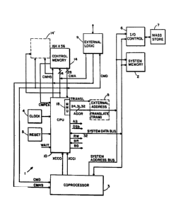
Fig. 1 is a block diagram showing a data processing
system 1 having a CPU 10 which is constructed and
operatQs in accordance with the invention;
'',''.':.' '
-10- ',~
,."'~``:
i32~ ~7
Figs. 2a and 2b are a block diagram of internal
registers and buses of the cPu lo;
Fig. 2C iS a block diagram of a Branch Unit of the CPU
10: ,
Fig. 2d iS a block diagram of the Memory Management
Uhit (MMU) 18 of Fig~ 2a;
Fig. 2e is a block diagram of the Status Register 70
and associated logic; . :
:: ,.
Fig. 3 shows the format of a microinstruction which is
stored in the external control memory 14 and which -
directs the internal operation of the CPU 10, the `~
microinstruction comprising a process field, a memory .
field, a condition code field and a branch field;
Fig. ~ shows in re detail the format of the process ~`
field of the microinstruction of Fig. 3:
. . . . ..
Fig. 5 shows in more d~tail the format of the memory
field of the microinstruction of Fig. 3; .
~. ",.
: . " .:,
Fig. 6 shows the condition code field of the ..
microinstruction of Fig. 3;
,."',.'-
-11- '''.. ,~
,''`'. '",.`
.',' ,,- ',' '; ' '
132~7
Fig. 7 shows in more detail the format of the branch
field of the microinstruction of Fig. 3;
Fig. 8 shows the format of the branch field for a
branch to next macroinstruction (BNM) branch field
opcode:
Fig. g shows in more detail the format of the branch
field for a microinstruction which includes a status
setting (SS) branch field opcode;
Figs. lOa and lOb show the format of a virtual address
and a physical address, respectively, which is employed
by the MMU 18 of Fig. 2;
Fig. lla shows the format of a typical address
tranælation entry (ATE) which is a fea~ure of the NMU
18 of Fig. 2;
`~
Fig~ llb dhows in more d~tail the format of the page
frame entry of the ATg of Fig. lla; and
,..
Figs. 12a-12d show various aspects of the timing states
of the microprocessor 10.
;'" :.' ,' ~
..., . .:-
-12- "
:. '.
~ ~,. . .
132~7
DETAILED DESCRIPTION OF A PREæ~RRED EMBODIMENT
AS an aid in describing the microprocessor of the
invention the description has been partitioned into
several sections, each being designated by a reference
letter (A-E). These sec~ions are:
A. Architecture
Al. Register Set `
A2~ Arithmetic Execution Uhit
A3. Status Register
A4. Instruction Fetch
B. Microinstruction Set
C. Address Translation
D. Processing States and Timing
E. External Intcrface
A. ARCHITECT~K~ ~
`" ~`'' `
Referring to Fig. 1 there is shown in block diagram `~
form a data processing system 1 having a Central
Processing Uhit (CPU 10) constructed in accordance with
the invention. CPU 10 in general executes assembly
language statements which, in a preferred embodiment of
thQ invention, are Virtual System (VS) assembly
,~. ,,,, -,., "
-, ~ , X ; , , ~ , "; ,, ", ,; i, ;" , , " ,
132~7
language statements of Wang Laboratories, Inc. of
Lowell, Massachusetts. CPU 10 is designed to
efficiently execute the vS assembly language
instructions set; however, it can also be used as a
general-purpose microprocessor. CPU 10 in the
preferred embodiment of the invention is fabricated in
a 2-micron CMOS process; the chip itself being housed
iA a 144-pin grid array package~ However, the
teachings of the invention may be practiced with other
microprocessor devices fabricated with any suita~le
processing and packaging technology~
Programs are written in the VS Assembly Language, or
macroinstructions. The macroinstructions, which are
described in the VS Principles of Operation, copyright
lg83 by Wang Laboratories, Inc~, call up routines
composed of microinstructions~ CPU 10 processes the VS
macroinstructions and executes the corresponding
microinstructions~
To increase the speed of macroinstruction proceæsing
CPU 10 fetches the macroinstructionæ in sequencQ from a
syætem memory 2 and places them in an internal prefetch ~` `
buffer~ The prefetch buffer stores up to four 32-bit
full-words, on~ of which is considered to be the
currQnt inætruction~ If the current macroinstruction
' .'
-14-
', ,'
;.'
132~ ~7
requires a program control branch, the contents of the
prefetch buffer are replaced with the specified
instructions. The microinstructions that execute the
functions requested by the macroinstructions are stored
in a control memory 14 which, in accordance with one
aspect of the invention, is external to the CPU lo
whereby the microinstructions may be accessed by
external logic 9 and, if desired, loaded, read and/or
modified. External access to control memory 14
preferably occurs during a time when the control memory
address and data lines are in a high impedance state,
such as during a reset or wait state condition.
External logic 9 may be another microprocessor and/or :
other circuitry coupled to the control memory address ~`
and data lines and which is operable for accessing
memory locations within the control memory 14~ The
microinstructions may be loaded from, for example, a `
maqnetic disk or from data received by a communications
bus from a local or remote location.
. ~ .;
Typically, a macroinstruction requires multiple
microinstructions to complete the requested operation, `-
but many macroinstructions require only one
microinstruction. The address of the current
macroinstruction's microinstruction routine is ` ;-
calculated from the macroinstruction's operation code
.'.'` - ~.
-15- . '' ~.
.
~opcode). CPU 10 fetches the microinstruction routine
from the calculated address and executes the
microinstruction(s). Control logic routes the
microinstruction operands from CPU lO's internal
registers or memory interface to an Arithmetic and
Logic Unit (ALU), which includes a pseudo-barrel
shifter, and returns the results to the appropriate
register or to external memory. After the
microinstruction routine is executed, control branches
to the next macroinstruction to be processed, and the
above sequence begins again~ A more detailed -
description of the execution of macro and micro
instructions will be provided hereinafter. -
System 1 also comprises a 32 bit system data bus and a
32 bit system address bus which couples CPU 10 to the
system memory 2 and also, in some embodiments of the
invention, to external accelQration logic such as a
coprocessor 3. System 1 also typically comprises a
cloc~ gQnerator ~ and a reset generator 5 which provide
timing and initialization signals, r~spectivQly, to CPU
10 . ,
-16- ;
~ ' ',:
'''"' ''.
1 3 2 ~ 7
In accordance with aspects of the presently preferred
embodiment of the invention, coprocessor 3 may be
coupled to the output of control memory 14 for directly
receiving and decoding the microinstruction stream as
it is fetched for execution by CPU 10. The coprocessor
3 may also be coupled, via cPu lo input signal pins -
XCco and XCCl, to cPu lo whereby coprocessor 3 is
enabled to directly set the contents of a condition ;
code register within CPU 10. These aspects of the
invention provide for a tightly coupled, synchronous
CPU~coprocessor interface. CPU 10 is also provided
with bus reguest and bus grant signal lines which -- -
provide for a loosely coupled, asy~chronous ` -
CPU~coprocessor interface. Furthermore, the ~ ;
coprocessor 3 may be coupled to the system data bus
such that, in accordance with one aspect of the -
invention, coprocessor 3 may read data from or store ` `~
data within the system memory 2 at an address provided -
by CPU 10. This aspect of the invention will be
discussed b~low. `
: ` ,', '
System 1 may also comprise an I/O controller 6 which is
coupled to the system bus and is also coupled to a mass
storage devicQ 7 for transferring data and programs -
between the mass storage device and the system memory
,.,: ,. :~ .
'-. '`~., .`'' ,'`
:;:
-17-
.~ .
132~ 1~7
2. Other I/O controllers (not shown) may couple data
communications devices, operator keyboards and similar
apparatus to the syst~m 1.
CPU 10 also comprises an internal memory management
unit (MMU) 18 which may be selectively enabled or
disabled from translating virtual memory addresses into
physical addresses. If the internal MMU 18 is not
employed an optional external address translation unit
8 may perform the address translation. "
Referring now to Figs. 2a-2d there is shown a block
diagram of CPU 10. CPU 10's internal architecture
includes an Arithmetic Bxecution Unit (AEU) 12, a
prefetch buffer 16, and the internal Memory Management
Unit (MMU) 18.
''.'', '
The A~U 12 includes a 32-bit binary Arithmetic Logic
Unit ~AL~) that performs logical and binary arithmetic
operstions, an ALU that performs eight bi~ binary-coded
decimal (BCD) operations, a 6~-bit pseudo-barrel shift
registQr, and various other registers which are not
shown in Pig. 2.
-18- ~ -
,, , '` .
'~` ~'`
132~7
In accordance with one aspect of the invention, the
architecture of CPU 10 enables CPU 10 to support either
24, 31 or 32 bit external addressing.
Externally, and in accordance with another aspect of
the invention, CPU 10 employs the 56-bit-wide control
memory 14. CPU 10 has 14 control memory address (CMA)
lines enabling the addressing of up to 16K locations of
stored microinstructions.
CPU lO's internal architecture includes four buses:
the A bus 22, B Bus 24, C Bus 26, and Effective Address .
(EA) Bus 28~ The A Bus 22 provides a path from
r~gister operands and ROM to the ALU and the 64-bit
pseudo-barrel shifter. The A Bus is also used to
transfer immediate operands from the control memory 14 .`
to the ALU shift register. The B Bus 2~ provides a : `
- .
path from ~arious register operands, including the ` :
memory address registers, to the ALU and shift ;"
regiæter~ T~e C Bus 26 routes the result of a AEN 12
.
operation bac~ to the internal registers or to external
mflmory~ The EA ~us 28 is used to transfer memory ` `
addrQsses and provides a path for either a memory
addreæs regi~ter or a BD/ D X-generated address to the
memory interface 30~ The EA Bus also provides a path
into the ~ffective Address Register (EAR) 32 which
capturos the memory address used during a given c~cle.
-19- ,,'` :,.. `"
: ,;' '-
~ 32~7
Al . REGI STE:R SET
The functional register bloc~s shown in Fig. 2 aredesQribed below in Table 1.
Table 1
Register Description
AEU 12 Arithmetic Execution Uhit. The AEU
performs binary arithmetic and logical
operations~ binary-coded decimal
operations, shift operations, and
generates BD- and 8DX-type effeQtive
address calculations. The AEU 12 also ~
supportæ hardware assisted multiply and "
divido operations.
` ' `
AT~ S~t 3~ MMU ATE Register Set. This register set
containæ four p~rmanent and sixteen
temporary rQgistQrs, ~ach of which
contains translation information and a ~ "
valid bit.
' ' '
- ~
.`. '.
` `
: :'':
.
: '
132~7
BDXR 36 BD/BDX Register. The BDXR stores the
base-plus-displacement (BD) or the -
indexed base-plus-displacement (~DX) sum
from the ALU. -
BMWR 38 Branch Multi-Way Register. The contents ~
of BMWR are used by some branching ;`
microinstructions as a portion of the
branch address.
.''.` ,.....
BSR 40 Barrel Shift ~Qgister. The BSR stores :~
the number of bit positions for the
shifter to shift. ;~;
CH ~ Current Half-Word. The CH register
contains ths half-word (2 bytes) of
macrocodQ curr~ntly being dQcodQd. ~ ;
DISP ~3 Displacement. The DISP ~3 stores a 16
bit address displacemQnt for thos
- macroinstructions which require sme.
EAL 106 Eff~ctiv~ Address Latch. The EA Latch
holds th effective address for
translation by the MMU 18.
~.
~ . . .
-21- ; :
... ... .
'.,:
, ".,~.....
~32~7
EAR ~2 Effective Address Register. In the
event of a trap condition, the EAR holds
the faulting effective address.
FR 44 File Registers. The file registers are :
32 directly addressable registers that
are accessible only by microcode
(microinstructions).
'
GR 46 General Registers. The genQral
registers are 16 registers that are
addressed by macrocodQ
(macroinstructions)~
IAD ~8 Instruction Address RegistQr. The IAD
maintains the starting address of the
curreRt macroinstruction~
::: : . . .
IMAR 50 Instruction Memory Address Register. `-
The IMAR contains the address of th
next instruction to be loaded into the
prefQtch buff~r for po~æible futur~
processing by CPU 10.
. . ... .
~ ~ .....
'" .
-22- -`
. . .
.~;
,"",'.~ ',:
..
132~7
IREG 52 Indirect Register. The IREG contains a
pointer into the General Registers 46. ~
~ .. '
MAR0 54 Memory Address Register o. MARo points
to the half-word (2 bytes~ currently
being processed by CPU 10. This
half-word is part of the current
macroinstruction. -
: . :
MARl 56, Memory Address Registers 1 and 2. MAR 1
MAR2 58, and MAR 2 ara general-purpose address ~ ~ ;
registers which also autoincrement and `~
decrement by ~ 4 and-4.
. ,~ '`
MDR 60 Memory Data R~gister. The MDR contains
the data read into CPU 10 from the
system data bus~ ` ` `
`:.' '
PMR 62 Program ~ask Register. The PMR contains
the condition codes that are set as a
result of certain conditions impased by
the condltion code (CC) field of a
microinstruction, as shown in Table 8
below~
.
, ~. "~ .
.:.,, ,. - '
,,: ' ~
. ~
...,. ~..
:: .''
132~7
ROM 64 Read-only Memory. The ROM contains
constants that are used by CPU 10 during
operation. The ROM 64 has outputs
coupled to both the A bus 22 and B bus
24 and is addressed by selected bits of
microinstructions which employ the
constants stored within the ROM 64~ One
feature of ROM 64 is that for a given
address RQM 64 can provide an output to "
either the A bus or the B bus, the
output data not necessarily being the
same. For e~ample, the RQM address 2
may provid~ the pattern rr~r~rl6 to
- .
the A bus while if the B bus is the
destination the ROM may provide the
pattern 5555555516. Such patterns are
utili~ d g ~ rally by the AEU 12 for
mas~ing ~nd as fill patterns for shift
operations~
O~
~ 32`~7
RING REG 66 Ring Register. A ring is a three bit
unsigned integer that indicates the -
process level of the current process. -:
The value of the RING REG 66 is used to
determine the occurrence of protection
violations.
.:
XRE6 78 Index Register. The XREG is used ~or :~
indexed address calculations.
., ,,, ,','
XL 68 XL is a 32 bit register which for ; -
multiplication stores the multiplier and ;
the least significant word of t~e `
product after the multiply. XL 68 is `
also us~d for di~ide operations. ;
~ ., :,. . .
XR 69 ~R is a 32 bit regiStQr on the A bus
æide of the AEU. XR StorQs the most :: `
~ ... ;. . ~
significant word of a partial product. `;
XR 69 is also used for divide
~. . . ,:
opQratioAs. ;.~
--25--' .- . -~ : "
, ". . :
::.. . .
132~7
SR 70 Status Register. The SR has 32 status
bits for indicating the results of
various operations and for modifying or
conditioning the results of other
operations. The SR 70 is shown in Table
2 below and in further detail in Fig.
2e.
RAM Stack A CPU 10 internal RAM Stack register -
file is made up of a directly
addressable 32-word by 32-bit structure
(FR 4~) and a 16-word by 32-bit
indirectly addressabl~ structure (GR `~
6). 256 full-words of externally `" `
provided register file are addressed ~ia
bits ~-31 of th~ sQlected MAR in the ` :`
XRF addr-ssing space, as will be
describQd below~ : ;
~ -
~ A2. ~ ARITH~TIC EXECUTION UNIT
: : .
The ArithmQtic ~xecution Unit (AEU) 12 comprises
arith etic~logic units (ALUs) and supports 32-bit
binary operations, supports both 8-digit and 2-digit
; BCD opQration~, provid s a 6~-bit ps~udo-barrQl
: ' ,, ' '
. . .
-26-
: ~ ~ - : ". ~:
~;~
1324~7
shifter, provides required status inormation (binary
carry, decimal carry, overflow, zero, sign, carry from
bit 21, and invalid BCD digit), supports full-word and
half-word multiplication, supports full-word division,
and to also functions as an address generation unit.
The Binary Coded Decimal (BCD) ALU complements the main
binary ALU and shifter, and accepts thQ same operands
(A, B, and C Buses). Its activation is caused by a
family of BCD process field opcodes, as will be `
descri~ed.
'','.'"'.`.:' .'
.
The BCD ALU accepts 32-bit values, eight 4-bit BCD
digits (long operations), or two 4-bit BCD digits with
the remaining bits zeroed (short operations) from the A ;~
and B Buses and generates a 32-bit output that is
driven onto the C Bus~ For tho short BCD ALU, the
: .: . . ..
upp r ~hreo bytes of t~e output to the C Bus are zeros.
For ~ub~rac~ion, the nine's complement of the A Bus
. .. . ..
value is added to the B Bus value. Tho appropriate
carry-in~borrow is det~rmined by the process field ;-
opcode. ~`
. `'''.,"`''
.
:` ' ,
-27-
:., .
.
. .
1324~7
status register (SR) 70 bits affected by the BCD ALU
are ALU (SR 12), DCA (Decimal Carry-Out (SR 15), and
DEC (Invalid Decimal Digit) (SR 18). The ALU status
bit is reset to O when the BDC ALU operation generates
an output of magnitude zero (i.e., a decimal O is
driven onto the C Bus as a result of an operation~.
The D Q status bit corresponds to the CA (SR 13) status
bit of the binary ALU. The DEC status bit (SR 18) is
an error flag generated by the BCD ALU when the BCD ALU
is activated and an illegal input digit is detected on
the A or B Bus. A digit is considered to be illegal if
its binary representation is lOlx or llxx, where x is a
"don`t care."
Two binary ALU operations are multiplication and -
division. Both full-word and half-word multiplication ~` `
are implemented~ Full-word multiplication takes two
signed 32-bit quantiti~s as input and produces a 64-bit
product~ ThQ multiplication hardware implements
Booth's Algorithm. Full-word multiplication uses four
registers: XR, YR, XL and SR. The three opcodes
r~lated to multiplication are MDSET, MUL, and SQLP, as :
will b~ doscribQd~
.
'`' ` ` `
-28- `
';..
. .
1 ~) 2 1 1 1 1
Half-word multiplication (HMUL) multiplies a signed
16-bit multiplier by a signed 32-bit multiplicand and
produces a signed 48-bit product. The multiplier is
obtained from the least significant half-word of the XL
register. The multiplicand is obtained from the A-bus
operand. The C-bus result of HMUL is the most
significant 32 bits of the product. HMUL stores the
least significant bits of the product in the most
significant half-word of the XL register 68. `
:'
Division takes a 64-bit dividend and a 32-bit divisor ~ -
and produces a 32-bit guotient and a 32-bit remainder.
Division uses the same registers as multiplication: XR, `
YR, XL and SR. The three opcodes related to division
are MDSET, SQLP, and DIV. `
:` :
After a di~ision operation, the specified C Bus operand `~
contains the remainder and XL 68 contains the
unadjustQd guotient. The SGN status bit indicates the
8ign of the remainder. The remainder may reguire
firmware ad~ustment after the DIV operation. The
firmware adjustment is described as follows: If the
sign bit of the remainder is 1, then add the diviæor to
the stored remainder to form the final remainder~
-29-
1 32~'17
When dividing a large dividend by a small divisor, it -
is possible to generate a quotient overflow, which
indicates that the quotient has exceeded a 31-bit
positive value. Quotient o~erflow may be detected in
two ways. First, overflow is indicated if the divisor
is less than or equal to the most significant word of
the dividend. If this is not the case, overflow has
occurred if the quotient is negative.
A3. STATUS REGISTER
' ~ `
CPU 10 comprises the 32-bit status register ~SR)70
having bits numbered SRO-SR31. Bit manipulation
operations and conditional branching are available for
all ætatus bits. All status bits ar~ set to zero by `~
POR (Power-Qn Reset). ~ : `
'' ` ` `' ` ``
RQferring now to Fig. 2e there is shown in block
diagram form the status register 70 and associated
logic. Status register 70 comprises a 32 bit register
having a plurality of condition inputs which originate
in the AEU 12 and the MMU 18. These inputs are related `~
to thQ condition of status bits ALU (SR12), CA (SR13),
PCA (SRl~), DCA (SR15), SGN (SR26), OVF (SR17), ALW
(SRl9), ALH (SR20), M2S (SR21) and MMISS (SR28). A
.: ;~` .
,'' '`'` ' ,..' '` ~
. .
:
-30-
~"~
" `
~32~7 :
plurality of load condition input signal lines are also
provided for latching in the state of status bits at an
appropriate time in a cycle~ Outputs of SR70 are
applied to a buffer, shown schematically as the buffer
140, which outputs those status bits which are applied
to other logic within the cPu lo. For example, the
ISET (SR29) bit is applied to the control memory branch
unit (Fig~ 2c). ~ -
.' "' .
A status bit select logic block 142 receives
microinstruction CDl bits 14:13] (Fig. 9) and
sequentially selects status bits for operations~ A
select output is applied to SR 70 and the selected bit
is applied to an ~ latch 1~, a B latch 1~6 or
directly to an operation logic block 148. operation
logic block 1~8 also receives as inputs
microinstruction CDl bits 11~:17] (Fig. 9) which define
the type of operation to be performed upon the selected
bit(s) as shown in Table 12 below. The output of A
latch 1 U is also applied to branch control logic as a
qualifying input for those branch instructions which -
test a status register bit, for example BF and BT
(Table 9).
: .
, "
,.:', ''' '
'',~'
' ,': ' '
-31- -.
' .`'''.'` ~ '
.',.` ': , ,
132~ ~ 17
The result bit output of operation logic block 148 is
applied to status register 70 for storage within the
selected status bit.
Table 2 describes the function of each status bit. In
accordance with another aspect of the invention, each
of the 32 status bits are branchable. Thus, CPU 10
microcode may use any of the spare status bits
(SRO-SRll) as branchable flags within routines.
` -' '''-
Table 2 -
Status Bit Description
(SRO) SPO Spare bit O
(SRl) SPl Spare bit 1
(SR2) SP2 Spare bit 2
`'' ' ' . '
(SR3) SP3 Spare bit 3 ~-`
~, '
(SR~) SP4 Spare bit 4
-32-
~,,
"' '`' ~
: . .
132~7
( SR5 ) SP5 Spare bit 5
(SR6) SP6 Spare bit 6
(SR7) SP7 Spare bit 7
(SR8) SP8 Spare bit 8~ SP8 is also used in the
formulation of condition code CCS.
(SR9) SP9 Spare bit 9~ SP9 is also used in the
formulation of condition code CCS.
(SRlo) SPlo Spare bit lo
. .
(SRll) SPll Spare bit 11
~SR12) ALU The ALU status bit is set to 1 to
indicate a nonsero magnitude result from :.
t~e A~U. The ALU status bit is set to O ~."
to indicate a zero magnitude result from .``
the AEU.
. .
: ,' " .`'.
`:.~' '
`,- :,`
, - ~ .
. .
--33-- : .
~, , .
."''.,.'"`'','. '.
132~ 7
(SR13) CA The CA status bit is the carry-out and
is also one of the carry-in choices for
binary arithmetic operations (binary
addition and subtraction). The CA
status bit is set ~qual to the carry-out
of bit 0 at the end of these operations.
(SR14) PCA ~he PCA (Page Boundary Carry-Out) status
bit is affected by binary addition and
subtraction operations. The P Q status --
bit is set to the carry-out from the
11th rightmost bit (bit 21) of the C
BUS . ' `'' " '' "
" '```'` ~'.' ,`
(SR15) DCA The DCA status bit is the carry-in and
is also the carry-out bit for decimal ; `
addition and subtraction process field " `
- operations. The DCA status bit is set ~
to I by four decimal process field : ~`
opcodes ~DAC, DACZ, DSC, and DSCO).
(SR16) SGN The SGN status bit indicates whether a
particular 32-bit value is positive or
negativ . The SGN status bit is set
equal to C Bus tO] by the AND, OR, XOR, `
. . .
' ',','..",.' ',''
~34~ -
132'14l~7
and shift families of opcodes. It is
also affected by the opcodes SQLP, MUL,
and DIV.
iSR17) OVF The o~erflow condition is iaffected by
binary arithmetic operations. The OVF
status bit is set to 1 when the carry-in
to result bit 0 `is different from the
carry-out of bit 0. Otherwise, OVF is
set to O.
iSR18) DEC The DEC status bit is set to 1 if a
decimal operation (DAC, DACZ, DSC, or
DSiOO~ encounters an invalid digit (A-F)
in eithQr the A or B Bus operand. The
DEC status bit is not affected by the "`
hardware when invalid digits are not
encountered. The microcode must preset ;``
DEC to 0 before tQ8ting decimal digits: -
thQ hardwarQ nQvQr SQtS DEC to 0.
``:
":'' '`,~.
'` ' '
`'''""~
-35-
`. ',: "
. ''.'' ::,' ''
.. ... .
132~ 7
(SRl9) ALW The ALW (Full-Word Alignment) status bit
is used to check full-word alignment.
The ALW status bit is set equal to
MARxr30] ORed with MARx131] whenever
MARx is used as a C Bus operand. (MARx
represents MARo, MARl, or MAR2 . )
', -', " `
(SR20) ALH The ALH (Half-Word Alignment) status bit
is used for half-word alignment ` ;
checking. The ALH status bit is set
equal to MARx131] whenever MARx is used ;'
as a C Bus operand. `
(SR21) M2S The M2S status bit is affected during a
cycle in which MAR2 is specified in the ~ ;
Address Select field~ M2S is SQt to 1
only when one of the following
:: , .
conditions~occurs: -
:-.,.:','
~AR2 - O and is decremented; ~:
.. ..
' ..',':.
MAR2 - FFFFFFFFN and is incremented by ``
l; or .~`
...
, ~ .
- : : , , .
: ~, ., . -
-36-
132~47
rrrr~H < MAR2 < ~ FH, and MAR2 is
incremented by 4.
M2S is set to o on all other operations
in which MAR2 is the selected address.
When a cycle that specifies MAR2 in the `
Address Select field immediately follows
a cycle in which MAR2 was used as a C
Bus operand, M2S is set as described `-
above but the current ripple operation `
and the previous MAR2 value are used. -
During a normal cy~le both the current ``
ripple operation and the current MAR2
value are Qmployed.)
SR22) MADD The MADD status bit indicates, in
accordance with one aspect of the
invQntion, the modQ of addressing. A
one indicates 31-bit addressing and a
sero indicates 2~-bit addressing. Also,
MADD being a on~ causes ACT procQss
field op~rations and BD/BDX mQmory field ;~
operations to zero thc most significant
bit of th~ C BUS result. MADD being a ~ -
``'' '.
~37~ ;~;
:.'`
132~7
zero causes ACT process field operations - -
and BD/BDX memory field operations to
zero the most significant byte of the C ~ .
Bus result.
SR23) STATE The STATE status bit specifies either a
user state or a system state. The user
state is indicated by STATE being set to
one; the system state is indicated by ~ ;
STATE set to zero. The CPU 10 uses the
STATE bit to check for write-protection
violations during write memory `
operations (protection trap on write if ; ``
STATE = I and the WP bit (in MMU entry) `
. - .
~ 1). STATE ~ 1 also enablQs protection
violation (PIVOM) traps. The STATE bit
is unmodlfiQd by the hardwar~. A copy ~`
of the STATE bit is providQd for ;
external use to the aforementionQd
support logic. `;
(SR2~) VM The UM ~Virtual Machine) status bit is `- ;
æet by the firmware to reflect the
condition in PCW.
' "'~ ~'" '"
'`''`'"`"~ ''' '
-38-
.:
, ,~'.
'`:` '`,.' ' ',
132~4~7
SR25) VMP~ VM PHYS Control status bit. VMPC
equaling one indicates that the outgoing
address is to be physical and,
therefore, the MMU 18 or external
translatio~ logic should be bypassed. No
part of the MMU 18 is changed when VMPC
is set to 1. When both PHYS (SR26) and
VMPC equal O the outgoing address is `
virtual and requires translation. VMPC
is also used in the formulation of the
state of the TRANSb ~translate) pin
output~ :
SR26) PHYS Physical status bit~ PHYS - 1 indicates
that the outgoing address is to be
physical, and therafore the MMU 18 or
external address translation logic
should be bypassed~ No part of the MMU ``
18 is changed when PHYS is set to 1~ ~
PHYS is also uæed in tho formulation o~ ~ -
the stat- of the TRANSb pin output.
'..
' .,:
132~4~7
(SR27) MMU The MMU status bit equaling a one
enables virtual address translation by
the MMU 18. The MMU status bit equaling
a zero disables MMU 18 address
translation. .
`' ~ ,
(SR28) MMISS MNU Miss status bit~ MMISS equaling ::-
sero indicates an MMU 18 hit of the -:
effe~tive address for a ;.`
microinstruction. Otherwise, MMISS ' . `
equals 1. . ~
.: . .
Ater a memory ~ield WIPE, as d~scribed ;.
below in thQ WIPE microinstruction, .
MMISS equalling a sero indicates that a ``
dif~ere~t or additional entry existed . .
having the:same virtual address .~ .
information; thereforQ. the operation `~.
was not succQssful. MMISS equalling a .
one indicates that no other entry
existed with the same virtual address ~ ~.
information~ .
- . . .
.
~: ' '- ''-: '-''
.. .. ..:
: ;
.
40-
, .
~; ~ .: .,',''''.
~ '; .'". . ' .
132~7 :
(SR29) ISET ~he ISET status bit is used by
microinstructions to control the
high-order bit for the 14-bit multi-way
microinstruction address created by BNM.
For normal execution, the microcode . -
~eeps ISET set to zero. .
(SR30) EXEC The Fx~C status bit is a BNM-time trap
bit. The microcode sets EXEC to a one
before leaving an EXECNTE instruction
via BNMX~ EXEC is checked on entry into . -
an EXECUTE instruction to ensure that .
there are no nested EXECUT~S. The .
firmware must reset EXEC to zero during :.
the BEX ~W~-timQ trap and whQnever MARO
is a C Bus operand~
. ~ . , ~ .. .
. ~ , ..
(SR31) DE~UG The DEBUG statu~ bit i~ a
. firmware-controll~d BNM-timQ trap bit~
: A BNM-time trap is acti~atQd if DEBUG is `:
.
sQt to a onQ.
' ,:
. ~ ;: ; ,'' .':,
, . .
.. ~ ,
.
~, : ~ .. .; '
, .. . ...
~32~4~7
A4. INSTRUCTION FETCH
Instruction fetch and preparation of macroinstructions
generally uses five registers, namely IMAR s0, MAR0 54,
IREG 76, IAD 48, and CH 42~
The microinstructions associated with macroinstruction
fetch and preparation are IF, BD, BDX, BNM, CH and -
CHREL. IF is a memory field opcode that fills the
prefetch buf~er. BD and BDX are memory field address
. . .:
selections that deplete the prefetch buffer. BNM is a
branch field opcode that also depletes the prefetch
buffer. CH and CHREL are A Bus 22 operands that i;
depl~te the prefetch buffer.
''' . `
CPU lO's instruction prefetch logic comprises a
circular prefet~h buffer 16. The buffer 16 consists of
four 32-bit full-word entries. Th~ microcode memory
field opcod~ IF initiat~s instruction fetches
(IFetch~), but IFetches are performed by the hardware.
There ar~ two pointers associated with the circular
prefQtch buff~r 16. The write pointer is derivQd from
IMARt28:29]. For a normal IFetch, the memory read data
locatQd at I~AR's ~ull-word virtual address is loaded
~ ,'. .,:
.`,"
-42- -
. . ..
,.. ''.: :'
~,~"~
13244~7
into the prefetch buffer 16 at the write pointer
location. An associated valid bit is set to 1, and the
buffer entry is ready for subsequent consumption. A
read pointer is derived from MARor28:29]. MARO 130]
determines which half-word of the full-word indicated
by the read pointer is to be the current half-word,
that is the 16 bits that are next in line to be
processed. `
MARO 54 always points to the current half-word, except
for a brief transition period (during buffer entry
consumption). At BNM-time (when interpretation of the
next macroinstruction begins), MAR0 54 provides the
least significant byte of the current half-word into
IREG 52 and provides the most si~nificant byte to
branch logic. When MAR0 54 is a C Bus 26 operand, ``
IFetches and buffer entry consumption are considered to
be illegal operations~ A multi-way branch to the
corresponding microinstruction stored within control
m~mory 1~ occurs instead. MAR0 54 is used as a C-Bus
26 operand before any operations invol~ing the prefetch ``
buffer 16 occur in order to clear the valid bits.
-43- `~
''"'"`
' ~ ''`: ` `
13244~7
The BNM family of branch field opcodes, the CH and
CHREL A Bus operands, and the BD and 8DX memory field
opcodes each consume one half-word and cause MARo ~4 to
ripple (increment) by +2. When consumption is mandated -
by CH, CHREL, BD, BDX, or BNM-type operations, the
following events occur, wherein one half-word .. ~ .
consumption operation is allowed per microinstruction. .
If the full-word buffer entry is consumed, the valid
bit indicated by MAR0 54 is reset to 0; the new current
half-word is latched; and MAR0 54 is rippled ~2 to
point to the next half-word
: . .
IFetches are inhibited when the buffer 16 is considered
full, that is, when IMAR 50 points to a location having ~ :
a valid bit set to a one. IFetches and IMAR ripples
are also inhibited after an IFetch Fault until MAR0 54
is reload~d. Whenever an IF is issued for a prefetch .
buffer that is already full, that IF will be ignored by
the hardware. Whenever MAR0 54 is used as a C ~us 26 `;
~, . .. .
operand IMAR[0:29~ receives C[0:291 while IMAR 130:31] `
remain at ~ero, all prefetch buffer valid bits are :` ;
reæet to zero, and IFLT is reset.
. ~ ,.
.`,'," ~ `
. .-. ..
' :'- .`
. .
. ..
-44- .. ;.;
. ,
1 3 2 ~ 7
There are two types of IFetch trap-handling mechanisms,
namely immediate (normal) and delayed (PBE). The
issuiance of an invalid address ( INVA) or the occurrence
of a parity error (MPAR) during IFetch is considered to
be an unrecoverable error from a microcode standpoint
and, thus, these occurrences generate an immediate -
trap.
The handling of fault conditions, such as translation -
faults or protection violations, occurring during ``
IFetch are postponed until that address is actually
encountered in instruction-stream processing~ In this
way, instruction fetches may be performed during BNM `
without the possibility of th~ IF causing a restart of
the entire macroinstruction. ThesQ delayed traps are ``
controlled in accordance with the following three
methods: -
.`` ''"'.
1. In the event of a fault condition during `
prefetch, the IFLT signal is activated. IFLT
inhibits subseguent IFetches and the setting
~f any prefetch buffer valid bit to 1.
-45- `
.. ......
1 3 2 ~ 7
2. At the access or consumption of each
half-word, the hardware checks the
appropriate valid bit. -
3. If the appropriate valid bit is a 0,
exception processing is required. If a BNM
operation is in progress, a sNM-time trap is
signaled; otherwise, a trap is signaled~
In the event of a process-level violation during an
IFetch, the STATE bit (SR23) is checked when the MMU 18 :
is cnablQd~ For a system using external translation
logic 8, the external STATE bit in the external logic ` `
is checked. If the STAT~ bit is 0, indicating the ,
systQm state as opposQd to the user state, IFLT is
- :. . .
; ignor~d; ot~erwise, traps are handled as described
above in steps 1-3. ~ `.- -
Sinde IF e~tends into the middle of a following `
: . .
~icrocycle and prefetch buffer 16 entry consumption ~ ;
starts at the begiDning of the current microcycle, thQ
. . ~
~ ~ first IFetch after the prefetch buffer 16 is emptied ~
- . - . . .
o¢curs at least two microcycles bQfore a consumption in ; -
order to bQ valid for that consumption.
~, .
~32~7
The instruction fetch hardware procedure is described
below in Table 3. Both the effective address register
EAR 32 and the MMISS ~SR28) status bit are updated.
Table 3
Step Action
.
1 AT IFetch, issue the IMAR 50 address.
2 If all valid bits = 1 ~the buffer is full), or
any three valid bits equal ~ and the previous
instruction was an IFetch (the buffer will be
full), then abort the instruction fetch. "
Also, inhibit Ifetch related address strobe
(AS), data strobe (DS) and data bus enable ;
(DBEN) signal pin assertions and inhibit the
s~tting of prefQtch buffer valid bits until a
prefetch buffer location is emptied. ;~ ;
`"~' `.'`
:',`,: `' ,'
` ', '',`
` .":
-47-
` -,. '.` .
. .
~ ;;
132~7
Or, if IFLT = 1, then inhibit all current and
further IFetch related assertions of output
signals AS, DS and DBEN. Also inhibit valid
bit setting and future IMAR rippling until
MAR0 54 is used as a C BUS operand.
Exception processing will take place at the ;
attempted consumption of the invalid buffer
.
location. '
`': ".
Otherwise apply the physical address to .
memory and read the full-word data; clock .`
the data into thQ prefetch buffer 16 location .~ .:
point~d to by IMAR 50 and update the .~ .
associat~d valid bit; then increment IMAR 50 .".
by ~
`'. ",.~ ''' '` ':
~ ICROINSTRUCTION SET ``.
-
.. ..
:~ R~ferring to Fig. 3 it can be seen that `~ .`
mlcroinstructions ~re 56 bits long and are comprisQd of
., .
four fi~lds and two parity bits: the procQss field,
condltion code fiQ1d, memory field, branch field, the
parity high bit, and parity lo* bit. The
,
microinstruction routin- for each macroinstruction
begins at an address that is a multiple of Qight~ A
48-
~. : , . .
... ..
132~7
corresponding microinstruction routine~s address within
control memory 1~ is determined by placing 002 after
the macroinstruction~s 8-bit opcode. For example, the
opcode for the MVI macroinstruction is 9216; therefore
the corresponding microinstruction routine's address is
49016. `~`
In accordance with an aspect of the invention, the
control memory 14 wherein the microinstructions are
stored is accessed 28 bits at a time, thereby :`
decreasing by one half the number of input signal pins
reguired.
:
The microinætruction process field is a 2~-bit field
that specifies the arithmetic, logic, and shift
operations that are part of every microinstruction.
The process field format is shown in Fig. 4.
Examples of the process field opcode are 1416 which
cau6es the contents of the A Bus 22 to be exclusively
ored with the B Bus 2~. This operation affects status
bits ALU (SR 1~ and SGN ~SR 16). This operation also
affects the "forced live" bits LCA and LOVF. There
are four live bits LALU, LSGN, LCA and LOVF, which
affect condition code operations. These live bits are
.. . .
. :
:,,'..-.
_~,9~
. ,' .
" ` ,'.,',: ~
1 3 2 4 ~ ~7
affected every microcycle ac~ording to their status bit
definition unless they are ~forced~ in accordance with
a particular process field opcode.
Another process field opcode is ACT (lF16) which adds ;
operands related to the address bus in accordance with
the state of the MADD status bit (SR 22). If MADD is
egual to one the most significant bit of the 32-bit -
esult is set to zero. This results in the generation
of a 31-bit address~ If MADD is egual to zero the most
significant byte of the 32-bit result is set to zero
which results in, in accordance with an aspect of the
invention, a 2~-bit addressing capability~ Thus, the
addressing capability of the CPU 10 may be readily
changed by changing the state of the MADD status bit~
.
The~A Bus 22, B Bus 2~, and C Bus 26 operands are each
32 bits in length. The operands for any entity less
than 32 bits in length are ormatted and filled. The A
and B Bus operands are input to the AEU 12, and the
reæult is stored in the C Bus operand. Immediate A Bus `~
operand valu~s are 8 bits long ~ImmediatelO:7]) and are
found in Proceææt~:ll]. All immediate ~alues are input
to the AEU via At2~:31]; A10:23] are sero-filled.
., , ' ,
" ",: ' :
-50- ' ~
;,~..,- ,,., .: , .
:',` .,'
132~
The process field opcodes (bits 0:5) control the
function of the AEU 12. In addition to arithmetic,
logical, and shift opcodes, there are six opcodes for
special instructions. The opcodes support both binary
and decimal operations. Both binary and decimal
operations are 32-bit operations.
Binary subtraction is a one's complement subtraction.
Two's complement subtraction can be performed by
setting CA (SR13) to one. Decimal subtraction is a
nine`s complement subtraction. Ten's complement ~.
subtraction can be performed by setting DCA (SR15) to
one.
Four decimal operations (DAC, DACZ, DSCO, and DSC)
result in 32-bit quantities~ The Decimal Carry (DCA)
(SR15) bit is used as the carry-out or carry-in. `
Decimal operations SQt the Decimal (DEC~ bit (SR18) to
one if an invalid digit (A-F) is encountered within the
A or B Bus operand. Decimal subtraction is always a B
Bus opQrand minus A Bus operand (B-A) operation, using
the nine's complement of the A Bus operand.
,, .
- - "
-51-
: .
132~47
m e shift opcodes specify the number of bit positions
that the 64-bit, pseudo-barrel shifter will shift the A
and B Bus operands~ The shifter has two 32-bit fields:
the A field and the B field. The shifter places the A
Bus operand in the A field and the B Bus operand in the
B field. The concatenation is shifted left by the
specified number of bit positions, and the resultant A
field (i.e., the 32 most significant bits) is the
shifter output.
For example, for a SHL4 opcode, the number of bit
positions to be shifted is four: therefore, the output
of the shifter is the concatenation of the 28 least
significant bits of the A Bus operand with the four
most significant bits of the B Bus operand (A14:31~
concatenated with B10:3]). Each shift-left opcode has
a corresponding shift-right opcode. To shift left, the
quantity to be shifted is in the A field and thc fill
bits are in the B field. To shift right, the quantity
to be shifted is in the B field and the fill bits are
in the A field.
,; ,,' ,~''
` ' ' '
' ',.,' .
-52- ~
" : , , ,
132~7
As can be seen in Fig. 5 and as described in Tables 4
and 5 the memory field is a s-bit field consisting of
three subfields: the address select subfield
(Memory[O:l]), the ripple/trap subfield (Memory~2:3]),
and the memory field opcode subfield (Memory~4:8]).
CPU 10 includes D and BDX type of addressing. A
base-plus-displacement (BD) address is generated as
follows~ The 12 least significant bits of the current
half-word, or displacement, are zero-extended. The
zero-extended current half-word is then added to the
contents of the General Register that is pointed to by
the four most significant bits of CH, or base register.
If the base register is GXO, zero is added to the
displacement~
-..
An indexed base-plus-displacement tBDX) address is
g~neratQd as follows~ Th~ BD sum is added to the
contents of the General Register that is pointed to by ~
the four least significant bits of XREG 66 (the index). -
If t~e least siqnificant four bits of XREG 66 are zero, ~;
the BDX sum is equivalQnt to the BD sum. A~ has been
prQviously stated, the MADD status bit (SR22) affects
thQ BDX result as follews: if MADD ~ O, the most
siqnificant byte will be seroed; if MADD - 1, the most `;
-53-
.' ." ~ ': , '. .
1324447
significant bit will be zeroed, thereby providing for
24 bit or 31 bit addressing capability.
The address generation hardware is incorporated into
the AEU 12. The AEU and data path are used for BD and
BDX address generation when they are not being used for
process field operations. A 32-bit BD or BDX s~m is
computed whenever necessary, and a Wait/BDx timing
state is inserted before the fetch o~ the BD~x)
microcycle. CPU 10 timing states will be described in
detail below in Section D.
For every microinstruction, an effective address is
generated. The address salect subfield controls the
source of address for a microinstruction cycle. The
ripple/trap subfield controls MAR rippling or full-word
and half-word alignment traps as shown in Tabl~ 4. If :
Memory[O~ is low, Memoryll] selects eithQr MARl or MAR2
as the source of the outgoing address, and the
ripple/trap subfield controls how the selectQd MAR is
rippled (incremented). When Memory[O] is high,
Memoryll] determines whether the BD or the BDX address
is genQratQd, and the ripple/trap sub~ield
(M~moryl2:3]) controls trap enabling. Full-word
alignment trap (FAT) becomes active if either EA~30] or
.,
-54-
2 ~ 7
EAt31] is set to 1. The ~alf-word alignment trap (HAT)
becomes active if EA[31] is set to 1.
Table 4
' "
MemoryDescription
Fieldoutgoing
10:3]Address Selection Ripple/Trap -.
O O O O MARI MARl is not rippled
O O O 1 MARl MARl is rippled ~
O O 1 0 MARl MARl is rippled +4 -~.
O O 1 1 MARl MARl is rippled +l : ``.
O 1 0 0 MAR2 MAR2 is not rippled . :~
O 1 0 1 MAR2 MAR2 is rippled -1 ~
O 1 1 0 MAa2 MAR2 is rippled +4 ~ ;
O 1 1 1 MAR2 M~R2 is rippled +1 `.`
`"`; :,
I O O x Generate BD address FAT and HAT are disabled
1 0 1 0 B~nerate BD address FAT is enabled `~
1 0 1 1 GQnerat~ BD address HAT ls enabled
~ . . .
1 1 0 x Generate BDX address FAT and HAT are disabled
1 1 1 0 G~nerate BDX address FAT is enabled
1 1 1 1 Generate BDX address HAT is enabled . `- `:
'-:. '... .
. , .
:'. ~ '- ..
-55- ,.. ``.
: ,.; ' '.' .:
,. : .
13244~7
It can be seen t:hat the address select subfield selects
the address that will drive the Effective Address (EA)
Bus 28 and will thus load the EAR 32. The four sources
of address are MARl 56, MAR2 58, the BD/BDX sum 36, and
IMAR 50. IMAR 50 is an address source when the
instruction fetch (IF) opcode is issued.
The memory field opcode determines whether or not an
address is driven off-chip. If the memory field opcode
is a no operation (NOP). no address is dri~n off-chip.
The IF opcode supersedes the address selection subfield
and gates the IMAR address to the EA Bus 28. Any other
memory field opcodQ results in the effective address or
translated effective address being driven off-chip. ~`
The memory field opcodes thus specify the memory
op~rations to be performed. There are three types of
~emory field operations: translation opcodes, internal ; `
M~U opcodes, and nontranslation opcodes. These opcodes
are desQribed below in Table 5
~:
'~` ': . '
-56- r`~ ~
132~7
Table s
MEMORY FIELD OPCODES
Memory -
field Operation Opcode Type
02 IF Instruction Prefetch Translation Opcodes ` .~
(opcodes .
that can issue both -
virtual `;
~ ~ ., ~ ,.. .
and physical addresses `
0~ RB Read BytQ
05 N~ Write Byte
07 WEND Nrite Byte Nith No Data
0~ RN Read Word .. .
09 WW Write Word ` .. ~
0~ WNND Writ~ Nord Nith No Data . : .
OC RH R~ad Half-Nord .. , ."
- i
OE RH~ R~ad Nalf-Word With Sign `. ~`
Extension ""``:`:
: :,. .:
NOæ No Op4ration No operation Opcode .~
:;.. :..
,
_57_ ::; ;.
. . . :
.,~
.,: . .
. ~, . . .
,
~244~7
11 WIPE write Individual Internal MMU Opcodes
(opcodes
Permanent Entry that control the MMn 18)
12 DATE Delete All Temporary
Entries
13 WITE Write Individual -
Temporary Entry
LRNG Load Ring Register
16 RTRAM Read TRAM Nontranslational Opcodes. ``
17 WTRAM Write Tram (opcodes that issue only .`~ .
18 TRCT Text (Read~ Reference physical addresses) -
and Change Table (RCT)
19 RRCT Reset RCT
lA RCT R~ceiv~ from Coprocessor
lB SCP Send to Coprocessor
lC RIO Read I/O
lD WIO Write I~O
lE RNX Read Word From External Register File (XRF)
lF WWX Write Word to XRF ' `
:; '.~: `
- .
; ~ ''`
,~
,~,``"`
:
1324~7
There are nine translational opcodes, that is, memory
field opcodes that can issue either virtual or physical
addresses. These are IF, RB, WB, WBND, RW, WW, WBND,
RH, and RHE. If the address is to be physical, the . .
PHYS status bit (SR26) must be set to I before the
opcode is encountered to ensure that the :
virtual-to-physical address translation facility of MMU
18 does not translate the address. If the address is ~:
to be virtual, the PHYS status bit (SR26) is set to O
to ensure that the virtual address is translated to a --
physical address~ Table 6 describes the function of . -.
each of the translational opcodes.
.
,'; ~` '` ,'
^ "`'``:
.~ .
'`'`~
-59- `-
.. ' ~;; ...','
.. ...
~2~1~7
TABI~E 6.
TRANSLATION OPCODES
0pcode Description
IF Instruction Fetch. IF is a memory read ;
operation that uses ~he address contained in
IM~R 50. The data read is directed to the
prefetch buffer 16 for subseguent
macroinstruction decoding.
RB Read Byte~ RB xeads the data from the byte
address indicated by the address selection
field. This byte of information iæ then -:
gated by alignment logic 72 to the least
significant byte of the MDR 60, and the three
most æignifi¢ant bytes of the M~R 6Q are set
to s~ro. ``
` ~ '',',
',' :"
.,
` . ' ` `.
: ' ~
. ' '
..., :
"', ;';,
132~7
WB Write Byte. WB writes the C Bus 26 data from
the process field operation to t~e memory
address indicated by the address selection
field. Data is taken from the least
siqnificant byte of the C Bus; all other C - -
Bus data is ignored. Al ignment logic 74
places the byte of data into the appropriate
byte location within the data bus based on
EA130:31] according to the following
criteria~ -
EA[30:31] C[2~:31] will be
signal pins: output on data lines: ~
o 0 D10:7] ~ ;-
O 1 Dt8:15] ,-``.,~
1 0 Dtl6:23]
1 1 D[2~:31].
~BND Write byte With No Data. WBND is similar by
Nrite ~yte except that CPU 10 supplies no
data ~CPU lO's data bus is tristatQd)~ In
accordance with an aspect of the in~entlon i`
the translation opcode WBND may be usQd for
operationæ in which CPU 10 generates a
de~irQd memory addrQss and the coprocessor 3
,. .. . ~
supplies the data byte to b~ written.
-61-
. .. . .
:, .... ... .. .
',.,.. :
132~47
RW Read Word. RW reads the data from the
full-word address found at the source
indicated by the address selection field.
The two least significant bits of addressing
information are ignored. The data is read
into the MDR 60.
WW Write Word. WW writes the C Bus 26 data from
the process field operation to the memory
address indicated by the address selection
field. The leas~ significant two bits of
addressing information are ignored. -~
WWND Write Word With No Data. WWND is
substantially identical to Write Word, `-`
except that no data is driven onto the syst~m
data lines. In accordance with an aspect o~ ~
t~e invention, WNND may be used for ~-
operations in w~ich CPU 10 generates a
desired memory address and the external
coprocessor 3 supplies the data word to be
written~ "
,, ..: .
'. ''.
:
', ',~' :'
-62- '~
'
,. :", ,~` '
132~7
. . ,
RH Read Half-Word. RH accesses a full-word of
data from the address indicated by the
address selection field. The least
significant bit of addressing information is
ignored. The half-word indicated by bit 30
of the address is gated to the least
significant half-word of the MDR 60, and the -
most significant half-word of the MDR is set
to zero.
.......
RH~ Read Half-Word with Sign Extension. RHE -
accesses a full-word of data from the address
indicated by the address selection field~
ThQ least significant bit of addressing
information is ignored~ The half-word
indicat~d by bit 30 of the address is gated
to the l~ast significant half-word of the MDR
60. The moæt significant half-word of MDR 60
is s~t to sQro if the updated MDR116] equals
. .,, :. . .
s~ro or is sQt to onQs if the updated MDR116]
.'':, . ..:
equals one~
. .
~ ``' ,; '' -,
. . .
,, .
.,
:~ . ".. ,~
.: -,: .:
.;
, . :. . .
`::''
",, ~', . .
~ . .... . .
`, '~
1324~il7
There are five memory field opcodes that control the
internal MMU 18. These are WIPE, DATE, WITE, DIE, and
LKNG. m e MMU 18 will be described in detail in
Section C below. Table 7 describes these five MMU 18
related opcodes.
Table 7
Memory Field Opcodes
Opcode Description
.
WIPE Write Internal Permanent Entry. WIPE
updates the permanent entry (one to
four) indicated by the two least
significant bits of the EA Bus 28~
Normal preparation or the execution of `~``
this instruction is to: ; -
1. Load C~0:29] with the page frame ~ -
data. ;
2. Mask off the two least significant
bits of the virtual address and
store it in a selected MAR.
'~ ' ' ~` '
-64-
'"' ' `
`, .'`
. .
1 3 2 ~ 7
3. Logically OR a 0, 1, 2, or 3 into
the sele~ted MAR to address a given
permanent entry.
If the virtual address information
matches that of any entry, the MMISS -
status bit ~SR28) is set to zero and no
write occurs. In all other situations,
the MMISS status bit is set to one.
DATE Delete ~11 Temporary Entries. D~TE
deletes (invalidates) all 16 MMU 18
temporary entries at once. -
,
WITE Write Individual Temporary Entry. WITE ` -`
updates a ~mporary, least recently
used, internal MMU entry. The virtual
addreæ~ is placed on the EA ~U6 28 (via
a MAR, for example) and the page frame
entry, which is loaded from the previous
C~0:29~, is the write data. The page
framQ entry is written to C~0:291 during
the instruction that immediatQly
prQcQdQs the WITE instruction. An - ;~
,
'' ': ',':
~,' - ,
-65- ` ~`
'`"'`.~
132~il7
attempt to write an entry for which the
virtual page number already exists in
any entry sets the MMISS status bit
(SR28) to zero~ In this situation, the
write does not take place. Otherwise, -
the MMISS status bit is set to one.
DIE Delete Individual Entry. DIE utilizQs
the virtual address on the EA Bus 28
(from a MAR) to specify the internal MMU
18 temporary and~or permanent entry to ````
be deleeed from the internal MMU. If no
matching entry exists, the MMISS bit
(SR28) is set to OAe, otherwise the
MMISS bit is set to zero.
, ~.
LXNG Load Ring Register. LRNG loads the
3-bit value from the previous C~2~:31] -`
into the internal Ring Register 66 for
internal MMU 18 translation.
`' `
. ` ` `
' :, :`.
''`` '`
`''" ~` .`'
132~ 7
External
ring information is contained generally
in external logic 8. A system having -
external addre~s translation logic
typically does not use this opcode since
the ring number is loaded into the
external logic by an XRF write opcode.
Systems ~sing the internal MMU lB may
utilize this opcode in addition to
loading the ring numbQr into the
Qxternal logic. Ct2s:3l] is preferably
loaded with the required data during the
instruction that immediately precedes ``
the LRNG. ~``;`
Th~r~ are ten nontranslation opcodes, that is, memory
fiQld opcodes that issue only physical addresses. `
.
Thes- are RTRAM, NTRAM, TRCT, RRCT, RCP, SCP, RIO, WIO,
R~X and NWX~ BecausQ the TRANSb output pin is driven
high ~hen any of these opcodes ars issued, all
addre~sQs ~s~ued from these opcodes are considered to
....
b physical addresses regardless of the state of the
PNYS status bit.
. ; .
. . ~ , .
~ ~ -
~ 67- ,~ -
: ', , ~
~ . . .
132~7
As can be seen in Fig. ~ the condition code (CC) field
is a 3-bit field that specifies either a NOP or the
condition code operation type. The condition code
format is shown below in Table 8. :;
CC10:2] specify the condition code operation type; the :
actual two bit condition code is held in the Program
Mask Register (PMR) 62. The five condition ~ode .
operation types are: arithmetic (CCA), logical ~CCL), `
unnamed ~CCR), status (CCS), and external (CCX).
''. ,. ` '
Condition code settings are based on liYQ status .`
conditions (status generated from the current cycle) :
and~or the status bits (live status conditions that are `
latched from the previous cycle) or, in thQ case o
ccx, the status o the external condition codQ pins
XCCO and XCCl. .
."
.
: .. ,
.... . .....
'' ,': ' `
-68- - . ;
: - . .
,." :..,.,",
..., .. ~- , ....
132ll4~7
TABLE 8
~.
Ccto:2] CC ffl e PMR 62 Definition . ,-
O NOP Previous CC No Operation :
.- :
1 cca o o LOVF - O and LALU - O - :
1 CCA O 1 LOVF - O and LSGN = 1 and
LALU = 1
1 CCA O 1 LOVF - 1 and LSGN = O
1 CCA 1 0 LOVF = O and LSGN - O and
LALU ~ 1 ` .
1 CCA 1 0 LOVF ~ 1 and LSGN = 1 .` -:
.....
2 CCL O O LALU ~ O
2 OCL O 1 ~ LALU - 1 and LCA ~ O
2 CCL 1 0 ~ LALU - 1 and LCA ~ 1 :`
3 CCR O O LALU--O and LCA - O
3 - CCR O 1 LALU ~ 1 and LCA - O
3 CCR 1 0 LALU - O and LCA - 1
3 QCR 1 1 LALU - 1 and LCA ~
1324~`~7
4 ccs o o SP8 = O and SP9 = O
4 CCS O 1 SP8 = O and ~P9 = 1
4 CCS 1 0 SP8 = 1 and sPs = o
4 CCS 1 1 SP8 = 1 and sPs = 1
7 CCX O O XCCO = O and XCCl - O
7 CCX O 1 XCCO = O and XCCl = 1 -
7 CCX 1 G XCCO = 1 and XCCl = o -
7 CCX 1 1 XCCO = 1 and XCCl = 1
, ',
All condition code functions except CCS reflect the ~
results of the current operation only. The SS branch -
field microinstruction (described in Table lla) or a ~`
previous process field operation has no effect on the :~ -
current condition code operation, unlesæ it is CCS.
CCS is only updated from the results of the previous
oper~tion. If the PMR 62 is specified as the C Bus
operand in the process field operation and a condition `~
code operation is specified, the condition code
operation will supers~de the process field operation. ::
` ., - ,, ,
In accordance with one aspect of the invention the
condition code t~pe CCX enables the setting of the
conditlon codes in PMR 10:1] from the input signal pins -` -
, ~, .. .
XCCO and XCCI. This mode of operation is especially - ~
''" ' :' .:
.: ; , .~ . .
_70
. . .
.: -: .
....
~'~
132~ 7
advantageous wh~!n the CPU 10 is operating in
conjunction with the coprocessor 3 in that it permits a
tightly coupled interface to be formed between the cPu
10 and the coprocessor. For example, the coprocessor
3, by controlling the state of XCC0 and XCCl, may
directly affect the execution of a CPU 10
microinstruction, such as the Branch with Condition
Code Chec~ (BCC) which will be described in Table 9.
As shown in Fig. 7 the branch field is an 18-bit field
that controls the modification of the microinstruction
counter (IC) and status bits. One of the additional
functions of the branch field is to perform the Branch
to Next Macroinstruction ~BNM) operations.
The branc~ field consists of two subfields: the Branch
Opcode subfield (Branch[0:31) and the Branch Address
subfi~ld (Brancht~:17]). For some operations which
will be described below thQ branch addresæ subfield is
differentiated into an A bit subfield (Branch [4:8])
and a Branch Address subfield (Branch ~9:171).
" ,'::
The five types of branch field opQrations are: branch
operations, branch to next macroinstruction tBNM)
opQrations, multi-way opQrations, subroutine
operations, and status setting operations.
., ~, ,
-71- ` ` ```
~321`~7
The branch operations, namely BU, BCC, BF, and BT are
described in Table 9.
TABLE 9
Operation Description
' . " .:
BU Unconditional Branch. BU branches
to the microinstruetion address in
Brancht4:17]~ .
BCC Branch With Condition Code Check. ~ .
BCC e~amines the condition code
mask, which is held in I~EG 52 ` :
tO:3~, and ~he condition code, (CC) ~-
whieh is held in PMR 62 tO:l~. The -`.~
,. . :,: .
eondition code selects onQ of the
IR~5 S2 bits~ For example, a CC of
O selects IREG[O]: a CC of 1 . "
seleets IREGtl~; etc. If the
selected IREG bit equals 0, then a
braneh to the microinstruction ~ :`
address in Brancht~:17] is
, --
', :, .:.
. -
-72- .
: ::
.. . .... .. .
=~
~2~7
executed. Otherwise, the next
microinstruction (IC+l) follows.
The operation of BCC inserts
Wait/BDX state whether or not a BD
or B~X is specified in the memory
field.
BF Branch False. BF tests thQ status
bit specified by the A Bit
subfield, Branch t4:8]~ If the
value of the selected status bit is
0, then the branch is takQn. The
branch address is formed by
concatenating IC+ltO:~] (the ive
most significan~ bits of the
increm~nted IC) with Brancht9:17]. , `
~ .
Conditional branches are limited to
a r~nge of 512 microinstruction ~ -
locations. `" ``
BT Branch True. BT tests the status
bit specifiQd by the A Bit
subf1Qld. If the valuQ of the
sel~cted status bit is 1, the
; : ~ . / .
~ 73_
..
~`''```~
13~ 17
branch is taken. The branch
address is formed by concatenating
IC+ltO:4] (the five most
significant bits of the incremented
IC) with Branch~9:17].
Branch to Next Macroinstruction ~BNM) prepares CPU 10
to process the next macroinstruction and enables the
processing of some exceptions, as will be described~ -
BNM operations ~heck for BNM-time traps, form a 14-bit ;`
multi-way branch address using the ISET status bit (SR
29~ and the current half-word (CH 42), set up IREG 76,
and load IAD 48 from MARO 54. ; .
:`'- . .
The BNM algorithm is describ~d in Table 10 for BNM -
opQration~ Some BNM commonly used operations (BNM, ~`
BWMX. BNMV, and BNMI) are impl~mented as
pæeudo-opcodes. The BNM opcode format is shown in Fig~ r"~''.`"
8~ The bits sho~n therein are defined as follows.
.;;
IRG i~ the En~ble IR~G ~pdating field. A one in EIREG " '
enables IREG updating; a ~ero in EIREG inhibits IREG
-,.'' ~
updating. .,;` ~`
~ - '"''``'"''
, .. :..
. . .
"'
~- ~74~ :~ :
: ~ ... ~
~: ,.. ,..'.. .' , . '.
: .', . -: .:
`~ =
1 ~ 2 `~ 7
EIAD is the Ehable IAD updatinq field. A one in EIAD
enables IAD updating; a zero in EIAD inhibits IAD
updating.
EBT is the Enable BNM-Time Traps Field~ A one in EBT
enables all BNM-time traps except Branch if Prefetch
Buffer Empty (BPBE); a zero in EBT inhibits all
BNM-time traps exc~pt BPBE~ -
..
EBOVT is the enable Branch if Overflow Trap (BOVT)
field. A one in EBOVT enables the BOVT trap; a zero in
EBOVT inhibits the BOVT trap.
,
TABLE 10. BNM ALGORITHM `:: :
Step Action ;
1 RIPPL~ MARO ~2
2 LOAD IAD ~8 ~ Load IAD 48 from the value
contained in MAR0 5~ beforQ the BNM. This `
opQration loads IAD 48 to point to the start :~
of thQ upcoming macroinstruction. The I~D 48
is not loaded if the BNM operation has EIAD -
O, or the LOVF status bit ~ 1 and EBOVT = 1, -~
or a trap is pending.
` ,.:,',',~
-75-
~ 3 2 ~ 7
3 Process the current half-word.
3a Create the 14-bit multi-way branch address.
. , .
3b If the indirect register (IREG) 76 = 1, move .
CH112:15] to the index register (XREG) 78 and ~- ~
mo~e ~H18:15] to IREG 76. :
4 TRANSFER CQNTROL ~ If any of the BNM-time
traps are active, vector to the BNM-time trap
handler~ The BNM-time traps are listed in .~:
Table 11. Otherwise, transfer control to the
microinstruction address generated in Step . .
3a.
. . .
``.' -' `. ' ..'
. .
; . ... .
. . .
,; ..
;.,.:
: `"'.,.,''.
,,,.; :..
~ ; 76 .~
1 3 2 ~ ~ ~ 7
TABLE 11
Source :~
Trap DescriptionInternal/External
BOVT Overflow TrapInternal
BEX Fx~CUTE Instruction Internal - `
BPMF Power FailureExternal "-
BET Event Timer External
BTIC Clock Int~rruptExternal .
BIO I/O InterruptEXternal .
BCM Control Mode External
BCOT Coprocessor External
BPBE Prefetch Bufer Empty Internal :.
BD~ Softwar~ Debug Internal .`
~ .
. .
: CPU 10 also includQæ a Status Setting ~SS) operation
h~ch provides the microcode with tho ability to affèct
sta~u~ bits. including thQ aforedescribQd spare bitæ
(SR0-SR9). Tho A Bit and B Bit fiQldæ each SQlQCt one .
of th~ 32 CPU 10 status bits. Th~ sel~cted ætatuæ bitæ
~ . :
are~ opQrated o~ in accordance with thQ status opcode,
and the resultant bit value is storcd in the B Bit
fl-ld. If a ætatuæ bit is alæo affQcted by a proceæs
. ~ . .
; ~ ~ . ...
~ 77_ ~ ~
. .
, ,.
~: ~ '.,: ,'.
132~7
or memory field operation, the SS operation will be
superseded. Barring any trap conditions, the next
instruction counter (IC) address is IC+l.
The format of the SS opcode is shown in Fig. 9 and is
described in Table 12~ ~
TABLE 12 : f
MNEMONIC OPERATION ~ -
~ESET . ~ ;
NOR A NOR B `
ANDNOT A AND B ` .
NOT B ` -
IAND A AND B
IVN A : .
XOR A XOR B
NAND A NAND B . :
AND A XNOR B
XNOR A AND B `~
MOVE A
ORNOT A OR B ``.
B :~
IOR A OR B
OR A OR B .
S13T 1 -, . , ::
-78- .
: -
13 2 `~ ~ `17
As can be appreciated, the SS opcode provides for the
value of any one of the status register bits, for
example the spare bit SR 1, to be logically modified by
the state o~ another status register bit, for example
MMISS (SR 28) and the result placed in SR 1.
Subseguent branch operations, such as sranch False (BF)
or sranch True (BT) may thereby transfer control to
other microinstruction locations~ Such status register
bit modification and conditional branching results in
the formulation of highly efficient and powerful
macroinstructions.
Referring to Fig. 2c there is shown in block diagram
form a CPU 10 Branch Uhit 120. Branch Uhit 120
compriæes a Control Address Latch 122 which has 14
outputs which define the CMA to Control Memory 14.
Control Address Latch 122 receives input from a
plurality of sources depending upon the type of branch
operation or the type of addresses currently being
employed. ThQ microinstruction Branch field ~Fig. 3)
is providQd to Control Data Qne (CDl) Latch 124. An
output of CDl ~atch 12~ is coupled to the input of
Control Address Latch 122, which also has output for
providing the Control Address to a Control Address
IncrementQr (CAI) 126. CAI 126 provides an incremented
:
-79-
'',.'~. ' '.
" ';.`., ``
132'~ ~7
Control Address to a Control Subroutine Stack (CSS) 128
when it is necessary to nest microinstruction addresses
due tQ the occurrence of transfer of control
instructions~ Control Address Latch 122 also receives
an input from a Nex~ Macro Driver 130 which has as its - -
input ISET (SR 28) and the MSB of the CH Register 42. `
Next Macro Driver in general provides the initial
address of a microinstruction or microinstructions ~
which correspond to a macroinstruction. Multiway `
Driver 132 receives an input from BMWR 38 and is `
employed for multiway branch operations~ Trap Vector
Driver 13~ receives an input which corresponds to a `
decode of all CPU 10 trap conditions and which therefor ^ ``
provides a microinstruction trap vector address for
accessing trap related microinstructions.
C. ADDR~SS TRANSLATIQN
,.,
Many data processing systems employing a data processor
are reguir~d to perform address translations for
certain memory field operations that access main
memory. In these circumstances, the effective address
must be translated from a virtual address to a physical
address before it can be used by main memory. CPU 10
can, in general, perform address translations in one of
:
'...' .. ,
.. . . ~
-80-
.
~ `'. ' .
: :' , ...
~ 3 2 ~
two ways: the cPu lo may utilize either the internal
memory management unit (MMU) 18 or external address
translation hardware such as a memory Translation RAM
(TRAM) . '
The internal MMU 18 may be used to perform address
translation for memory field operations that access
main memory (opcodes Oxxxx). These operations include
memory read, memory write, and IFetch operations. If
the MMU 18 performs an address translation, the
effective address is translated before it is driven
off-chip. The operation of the internal MMU 18 is
described below.
CPU 10 also supports the use of external hardware for
addr~ss translation. If external hardware is to
perform an address translation, the untranslated
effQctive addr~ss is driven-off chip and is translated
ext~rnally~ Th~ external address translation hardware
may b~ constructQd in a number of fashions and may
includQ a tablQ loo~ up type of translation means, such
as a table stored in RAM. Certain microinstructions,
8UCh as RTRAM and WTRAM, and output signals, such as
.
TRANSb, support the operation of ext~rnal addr~ss
translation hardwar~.
``.' . '-,",'
, .. .
-81
,`..".; ':-:'
1 3 ~ 7
The MMU status bit (SR27) specifies whether or not the -
MMU 18 is to perform address translations. If the MMU
status bit equals a one, the MMU performs address
translations for certain memory field operations under
conditions which will be specified below. If the MMU -
status bit equals a zero, MMU 18 performs no address
translation and address translation, if any, is `
performed by external hardware.
. ~.. ~, ,.
In general, the address formats of the internal MMU 18
may be used to define and control the translation of an
effective memory address from a virtual address to a ~`
physical address for certain memory field operations~
The formats of the virtual and physical addressQs when
the ~MU 18 is used for addrQss translation are shown in
Figs. lOa and lOb, respectively.
' ' '
In general, th~ MMU 18 translates the effectivQ address
by r~placing a 21-bit virtual pagQ number of Fig. lOa
with a 21-bit page frame number of Fig. lOb. The
address offset into the page remains unchanged by the
translation. ``
~ ~ . - .,
The information requir~d by the MMU 18 to perform
addr~ss translations is stored in the form of Address ~;
.`''
. .
... .
-82- ~`
, . .
;,...
132~ 7
Translation Entries (ATEs) in ATE Register 34. Each ATE
contains the virtual page number, page frame number,
ring number, and write protection bit of a virtual page
of main memory. :
Both the virtual page number and the page frame number
are 21-bit unsigned integers~ The ring number is a
3-bit unsigned integer that specifies the lowest
process level that is allowed to access the page for a
read or a write in the user state (STATE status bit ~SR
23) equals 1). The write protection bit is a single .
bit that indicates whether or not the page is
writ~-protected~ If the write protection bit equals 1,
th~n the page is write-protected; otherwise, the page
is not write-protected~
~, '.`~
T~Q MMU 18 in the preferrQd embodiment of the invention ` . .
stores up to 20 ATEs~ In accordance with one aspect of
the invention, four of the AT~s are considered
permanent and æixteen are considered temporary. The
storage of AT~s in the MMU 18 is controlled by
microcode using thQ aforedescribed m~mory field ;;
operations WIPF, WITE, DIE, and DATE. For example, the ::
permanent ATE entries may advantageously be employed to .
store translation data relating to the operation system
~"'', :" '
. .'., :'~':
-83-
.,.:.'' .~:
'.~,'. ~','
1321~7
(os), thereby enabling the OS to execute more
efficiently since it will not be frequently ~swapped
... . . .
out" to make room in memory. The sixteen temporary ATE
entries are managed by a ~least recently used" (LRU)
memory management technique to eliminate, when
necessary, an entry or entries which have been loaded
the longest and which have been least recently used for
an address translation~ This LRU algorithm is
implemented by a stack mechanism whereby an ATE entry
that is utilized for a translation is removed from the
stack and reinserted àt the top of the stack, the stack ~ `
being pushed down to make room for the entry moved to
the top. It can be appreciated that this technigue
ensures that the entries at the bottom of the stack ~`~
have least recently been accessed~
For eaoh microinstruotion, the MMU 18 assumes that the
~ffective addrQss is a virtual address and compares the
virtual pagQ nu~ber of the Qffective address to the
virtual page number of eaoh ATE stored in the MMU 18.
If the ~irtual page number of the effQctivQ address
doQs not equal the virtual pagQ number of any ATE
storQd in the MMU 18, th~n an MMU mi~s condition is
said to QXiSt for the microinstruction; otherwise, an
~MU miss condition doQs not exist. Thus, an MMU miss
'`''' ~'''`''' ''
-84-
.
. ~ , .
132~7
condition indicates tha~ no ATE is available in the MMU
18 to translate the effective address. In this case,
the page frame information (physical addresstO:20])
which is driven off-chip is set to zeroes.
For each microinstruction, the MMU 18 modifies the
MMISS stat~s bit ~SR28~ to indicate whether or not an
MMU miss condition exists for that instruction. The
MMISS status bit is set ~o one if a miss condition -
exists; otherwise, the status bit is set to zero, This
condition occurs for every microinstruction regardless :"
of whether or not the MMU performs an address
translation.
On each microinstruction, the MMU 18 translates the
Qffective address if, and only if, each of the `
following conditions exists: the MMU status bit (SR 27)
~guals 1 (prior to instruo~ion exQcution); both the
UMPC (SR 25) and PHYS (SR 26~ status bits egual 0 `
(prior to instruction QxQcution); and ~he memory field
opQration is a main memory access operation (opcodes
O~x) . ; ~`' '
' '` ' ` ~'`', '
'~''', ." .
~. , :", :,.
-85- `~ ~
,
'.' ' '
-
1 3 2 ~ i7
As has been pre~iously stated, when equal to 1 the VMPC
and PHYS status bits indicate that the effective
address is already a physical address and thus suppress
translation of the address by the MNU 18.
On each microinstruction for which the MMU 18 performs
an address translation the translation is successful if
an MMU miss condition does not exist~ In this case,
the physical address is evaluated from the ATE that has .
the same virtual page number as the effective address. . .
The physical address is evaluated using the format
described above in relation to Fig. 10~
For each microinstruction for which the MMU 18 performs
an address translation, the translation is unsuccessful `
if an MMU miss condition exists~ In this cas~, the
effQctive addrQss is translated into a physical address
consisting of all ZQros, and this physical address is
driven off-chip. For each of these microinstruction
for which the ~MU 18 performæ an unsuccessful address
tranælation Qither a MISS trap or an IFLT condition is
signalQd. An IFLT condition is signaled if the memory
field operation is an IFetch operation; otherwise a
MISS trap is signalQd. Output signals data strobe .: .
(DS) and data bus enable (DBEN) are inhibited when an
MMU miss condition is detected.
-86-
!;;
., ,
1 3 2 '~ 7
On each microinstruction for which the MMu 18 performs
a successful address translation a protection violation
occurs if either one of two conditions is found to
exist. One, if during a read operation, the STATE
status bit eguals one (prior to instruction execution)
and the read ring number of the ATE is greater than the
ring number stored in ~he internal ring register 66,
or, two, if during a write operation the STATE status
bit equals one (prior to instruction execution) and the
write ring number of the ATE is greater than the ring
number stored in the internal ring register 66. As has `
been previously descri~ed~ the STATE status bit ~SR 23) ` -
indicates whether the current process is in the user or ;
the system state. The process is in the user state if
the STAT~ bit equals a one, and in the system state if
th~ ST~T~ bit equals a sero. The internal ring
register 66 con~ains the ring number of the current
process~ Its value is set by microcode using the LRNG
memory field op~ration as has been previously
described. ~ ..
If, on a given microinstruction, the MMU 18 performs a
succesæful address translation while the STATE status
bit equals a one and a protection violation occurs,
then either a RPVM trap, WPVM trap, or IFLT condition
, :',. .:
. .
-87- ` `
~32~ 7
is signaled. An IFLT condition is signaled if the
memory field operation is an IFetch operation; a WPVM
trap is signaled if the memory field operation is a
memory-write operation (opcodes 0xxxxl). Otherwise, a
RPVM trap is signaled. In all of these cases, the
output signal DS is not generated. If the STATE status -
bit equals sero, no protection violation trap occurs.
The ATEs are stored in the twenty registers
collectively designated the ATE registers 34~ Each ATE
stored in the MMU 18 is stored in a separate ATE `
register. At power-on reset (POR), each ATE register
is initialized to be empty. After POR, ATEs are stored
in the ATE registers only by the execution of the WIPE "
or WIT~ memory field operations, as specified above. i~
AT~s can be deleted from the MMU 18 by using the DIE or `
DATE memory field operations, also as specified above.
Fig~ 2d sho~ the MMU 18 in greater detail wherein it
can be seen that th~ AT~ registers 3~ are comprised of
a sQt of Page Frame Entry Registers 100 and a set of
Vireual Pag~ Number RegistQrs 102. Register Set
Control Logic 10~ manages the operation of the ,;
afor~describ4d least recently used ATE storage
algorithm, manages th~ control of the MMISS status
. , .
--88--
`: -, . . ' -.,
132~
register bit (SR 28) and the other functions described
which are related to the operation of the MMU 18. The
EA bus 28 is coupled to an Effective Address Latch 106
which provides latched effective addresses for storage
in a Virtual Page Number Register 102. Data Latch 108
is also coupled to EA bus 28 and supplies latched data
for storage in Page Frame Entry Register 100 and ~ing
Register 66. An output Address Latch llo receives .~
addresses from three possible sources and drives the `
System Address Bus.
` ,':
As has been stated, in accordance with one aspect of
the invention there are two types of ATE registers~
permanent and temporary~ There are four permanent ATE
registers and sixteen temporary ATE registers. The `
differencQ between the permanent and temporary .-
registers is the manner that the WIPE and WITE
instructions store ATEs in the registers~ As far as .
addreæs translation and the determination of the MMU
miss condition are concerned, there is no significant - ``
difference between those ATES stored in the permanent
and temporary ATE registers.
''`',`'',``', :.
. ,, :.. ... .
''.'..
-89- :
.
, ~.,
132~ 7
The WIPE and WITE memory fields operate to store ATEs
in the MMU 18. For either operation, the virtual page
number of the ATE is determined by the effective
address according to the virtual address form as given
above in relation to Fig. lo. The page frame number,
ring number, and write-protect bit of the ATE are
determined by the data from the previous C BUS
2610:29]. This data is called the page frame entry.
The formats of an ATE and a page frame entry for the
WIPE and WITE operations are shown in Figs. lla and
llb, respectively.
'`"'.
The WIPE operation stores t~e ATE in a permanent ATE
register. The permanent ATE registers are numbered
from 0 to 3. The register in which the ATE is stored
is specified by the two least significant bits of the
effecti~e address; LEA t30:31] which are input ta
Register Set Control Logic 10~.
ThQ WITE operation stores the ATE in the least recently
us~d temporary registQr. A temporary register is
considQred to be used when eith~r an ATE is stored in ` `~
it using th~ WIT~ operation, or the register is full
~nd th~ ATE stored in it is used for address
translation.
.
:.
....';'' ` ' `
' .
132~-~i7
The MMU 18 does not perform a WIPE or WITE operation if
it could result in two ATEs being stored with the same
virtual page number. Specifi~ally, an ATE is stored by
either a WIPE or a WITE microinstruction only if an MMU
miss condition (SR 28 = 1) exists for the
microinstruction. If a WIPE or WITE memory field
microinstruction stores an ATE in an ATE register that
was full before the operation is performed, the ATE
previously stored in the register is effectively
delet~d from the MMU 18. Issuing a DIE instruction,
described bQlow, for the page to be written before a
WIPE instruction ensures that the entry is loaded
within an ATE register.
The DIE and DATA memory field operations are utilised
to delQte ATEs from the MMU 18. The DIE operation
deleteæ any ATE that has the æame virtual page number ``~`
as the effective address using the virtual address
format given above~ If an MMU miss condition exists
for the microinætruction, then no ATE is deleted. If
an MMU misæ condition does not exist, then the ATE is ~
deleted, and the ATE register that Qontained the ~`
deleted ATE becomes empty. The DATE operation deletes
all ATEs stored in temporary ATE registers, thereby
causing all temporary ATE registers to beQome empty. "~
--9 1--
""' '"'
... . ..
. . . .
1 3 2 ~ 7
To check the contents of the MMU, all 220 possible
entries may be tested using the TIE pseudo-opcode
(NOP). The TIE memory field pseudo-operation tests for
the existence of an ATE with a specified virtual page
number. The virtual page number is specified by the
effective address according to the virtual address
format given above. This pseudo-operation is
implemented as a memory field NOP operation, and the
existence of the ATE can be determined by examining the
MMISS status bit (SR 28) after the operation.
As has been stated, the ring register 66 is used to
store the ring number of the current process~ The ring `
number is a 3-bit unsigned integer that indicates the
process level of the current process, and is used to
determine the occurrence of protection violations. The
value o~ the internal ring register can be written only
by the LRNG memory field operation. The LRNG memory `~
field operation stores the previous Ct29:31] in the `~
internal rinq register.
. '` :,
The aforementioned external addresæ translation logic
may determine whether or not a given memory field
reguires address translation by examining the memory
field operation at the control data pins. In an
:
~ "
-92- :- `
` -
32 ~
external translation system, if the TRANSb pin equals
zero, then translation is required. If the TRANsb pin
equals one, no translation is required.
D. PROCESSING STATES AND TIMING
In a preferred embodiment of the invention a basic
microinstruction cycle is 210 nanoseconds in duration.
As can be seen in Fig~ 12 each 210-nsec cycle consists
of two 105-nsec timing (T) states. Each los-nsec T
state consists of three 35-nsec ~hi states. The first
of these T states is the Fetch state and the second is `-
the Store state. The basic timing is derived from a
C~OCK input to CPU 10. :~
Th~ procesæ and branch fiQld operations span from the
start of a Fetch state to the end of the ensuing Store ;
state. This time æpan defines a microcycle. Memory
field operations start at the beginning of a Fetch
state, and thQ memory cycle ends at the completion of
th~ next FQtch state, provided no Wait or Bus Grant
states are encountered.
:,.-..,','.'~ .. '
-93- ~ -
`'..' '",' '.
1324447
CPU 10 has nine timing states: Init, Fetch, store,
Wait/BDX, sus srant~ Pre Bus Grant, Arith, Trapl, and
Trap2. Table 13 describes each of these states, which
are also illustrated in Figs. 12b-12d.
Table 13
State Description
~ .
Init The Init state is the starting point of
execution for CPU 10. In this state, .
all hardware initializations take place.
Init is entered on the occurrence of a
high-to-low transition of the RESETb ` -
input~ During the Init state, the clock ; -
is ignored~ When the RESETb input is ~
deactivated, the TRAPl state is entered. - -
:
Fetch The Fetch and 8torQ states normally
define the microcycle, of which Fetch is
considered to be the start. The
process, memory, and branch field ::` `
operations start in the Fetch state.
The mQmory field operation usually
finisheæ in the Fetch state. The Fetch
state is normally entered from and ~``
followed by the Store state.
-94- : ;
~.,~-,
132~
Store The Store state is the normal completion
of a microcycle. The process and branch
field operations finish in this state.
The Store state is normally entered from
and followed by the Fetch state.
`- '~
Wait/BDX Wait states are inserted after the Store -
state to delay the completion of a
memory or other Qxternal cycle. Wait
states are generated as long as the `~ -
WAITb input signal pin is active. The ~ ;
BD~BDX sum is also generated in this ~ " ;
state~ During the Wait state, the CMHS
signal pin is tristatQd to allow, if
d~sired, an external device to rQad the "
contents of control mQmory~
` . .' .
BU8 Grant ~he Bus Grant state tristates data
signal pins[O:31] and asserts the Bus
Grant ~BG) output signal pin. Bùs Grant `.
states are generated as long as the Bus ``~
RequQst (BRb) input signal pin is
activQ. ~us Grant states always follow - ;~
the Pre Bus Grant state and are followed ` -
by the Fetch state.
_95~
;: :
. :::
132~7
Pre Bus Grant The Fetch state normally completes the
memory cycle. If, after the completion
of a microcycle (after the Store state),
a bus grant is to be issued, ~he memory
cycle must still be completed. A Pre
Bus Grant state is inserted between the , -,
. .. .
Store and sus Grant states or between
the Waît/BDX and Bus Grant states in ` - `
order to complete a current memory
cycle. '' "
. ,, :
,Arith The Arith state performs the shifts and
adds for multiplication. It is ` `'
selectively repeated, followed by the
store statQ. The Arith state follows
the Fetch statQ~ `',
The Arith state also performs the shifts ' '
.
and addition~subtraction for the
restoring division algorithm. It is
. . .
selectivQly repeated and is followed by - ~-
,- ~, - . .
~ ~ th~ Store StatQ. i,;,
.. .. .
. . .
~ 96~
,
, . . .
;: .. :
-- 1 324~7
Also, the Arith state may be inserted
to provide an extra state that provides
the additional time needed to perform
BCD operations.
Trapl The Trapl state is the first state -
entered for processing a trap. During `
the Trapl state. the TRAP signal is
cleared, either the trap vector address
or the PECM vector address (depending on
which signal is active) is loaded into
the instruction counter, and a control
memory read cycle is started (as in
. ., ' '
Fetch). If both signals are active, the `
PECM address takes precedence. Trapl
reenables EAR 32 updating and DS output
signal g~neration. Future traps are `~
inhibited until a BMW, with the inhibit
; INH bit egual to 0, is issued. The '```
IRPIPl stat~ always ~ollows the Fetch
s~ate and is always ~ollowed by the ; :
Trap2 state. ~
.,j.,,,,~,.... .
. ~
`' ~ "'
_97_ ~ -
. .
.' . .. '.:~
" " "`" ,.
132~447
Trap2 The Trap2 state is similar to a Store
state~ The control memory 14 is accessed
and microinstruction decoding is - -
started. The Trap2 state always follows
the Trapl state and is always followed
by the Fetch state.
In accordance with another aspect o~ the invention CPU
10 is operable for providing on the system address bus,
at a time when the bus is not required to convey
address information to the system memory 2, the result
of a previous AEU 12 logical, arithmetic or shift
operation. This capability facilitates diagnostic
operationæ wherein the A~U 12 may be directly monitored
by observing the system address bus during the
appropriate portion of a cycle. This AEU 12 result
data is provided during the Phi 2 statQ of the store
portion of a cycle. thQ main memory addrQss having been
prQviously pro~ided som~time during the preceding fetch
portion of the cycle. Inasmu~h as the address strobe
(AS) signal is t~pically utiliz~d to latch the address
bus, th~ addr~ss bus may ther~after be utilised to
convoy tho A~U 12 result information. The AEU 12
r~sult i8 coupled to the EA bus 28 and is dri~en onto
th syst~m addrQss bus.~ The Trap Strob~ output signal
: ....
. .
.
- ~ -98- ~
,`- .
,..:. '
132~7
line (Table 14) is asserted during the Phi 2 portion of
store in order to la~ch, if desired, this AEU 12 result
information within external hardware.
E. EXl~NAL INl~EAOE
.:
m e CPU 10 external interface signal pins are shown in ` ~-:
Table 14. ``
, `' ';
Table 1~ CPU 10 Signal Descriptions ~
-., , ` '.
Pin Input~
Quan-
tity Signal Output Description
8 ~DD I Power -~
VSS I Ground "~
1 CLK I CLK is the input from a crystal
oscillator having æix times the ;~
microcycle freguency of CPU 10. `
1 CLCROUT O CLgOUT is asserted during Phi 3 `-
of each state. -
1 WAITb I A low on WAITb at the end of
the Fetch state causes MCU 10
to enter a succession of Wait `
states, from which it does not
exit until the Waitb input is :~
driven high. `
_99_ . . . - .. : .
", . '
1 3 2 ~ 7
1 RESETb I A low on RESETb puts cPu lo
into an INIT stat~. While the
RESETb input is active, all
trap and sNM-time trap signals
except INIT are set to 0. The
INIT trap is set to 1 until it
is recognized. Also during the
Init state, all status bits are
set to O~ `
1 BRb I A low on BRb indicates that a
bus request from another device ``-
has been received. When rQady, ` `
CPU 10 en~ers the Buæ Grant
State. `
1 BB O A high on BG indicatQs that CPU
10 has QnterQd the BUS Grant
state and has triætated the
~ appropriat~ outputs. `;~ 1 TSb O Trap Strobc iæ used by Qxternal
loglc to strobc certain
extcrnally generated trap
~ignals. Trap Strobe is also
used, as dcscribQd abovQ, by
external logic to latch the AEU
12 rcsult data appearing on the ~; `
; system addrcss bus.
: ~ . ,. ', ` .- '
1 0 0 ' `", ' '
!
132~7 ~
2 XCCO I XCCl and XCC2 receive a
condition code setting from an
external source, e.g., a
coprocessor. M
1 TRANSb O' In a TRAM system, TRANSb --
indicates whether or not - -
translation is needed. A o on ~:-
TRANSb indicates that
translation is reguired. A 1
on TRANSb indicates that
translation is not required. ``~
For a system using MMU 18, `
TRANSb - O indicates the ~`
occurrencQ of an MMU 18 miss
; condition when translation was
: .. :.'
reguired. The logical state of
T~ANSb is a function of status `
bits MMU (SR 27), PHYS (SR 26)
; VMPC (SR 25~ and MMISS (SR 28)
in con~unction with memory
fiQld opcode bit sQro~
1 XTRAP I A high on XTRAP during the
Fetch state causes CPU 10 to
~` enter a sQries of Trap states.
.. ..
~ . ~
: ~ .....
~ ` , .. ,, .. ,:,
132~47
1 DTRAP I DTRAP indicates a data error
caused by a CPU lO memory
transaction. A high on DTRAP
during the Fetch state causes
CPU 10 to enter a series of
Trap states~
1 XBTRAP I A high on XBTRAP during the end
of thQ 8torQ state immediately
preceding a BNM causes the
instruction counter to be
loadQd with the BWM-time trap ;;
v~Qtor . . '-
1 XIFLT I ~ high on XIFLT indicates that
a trap condition exis~ed during
an IFQtch.
1 R~ O RW indicate~ the direction of
flow of DSb.
: 32 ~ ADDRtO:311 0 The address output lines
(ADDR[0:3l])~comprise ~he main : `
` addressing interfaQe to the ~ -
remainder of the system.
: .. ...
: ADDa[o:31~ al~o conveys the
result of a pre~ious AEU 12 `.
op~ration~during the Phi 2
portion of the store portion of
cyc e. ~ ;
132~4~7
1 AS O Address strobe is used to latch
the address off-chip for data -
memory, I/0, XRF, etc.
opera~ions .
32 DATA~0:3l] I/0 The bidirectio~al data lines
(DATA[ O: 31]) comprise the main
data interface to the rest o~
the system~
l DSb O Data Strobe is used to clock
the data off-chip for data
memory, I/0, XRF, etc. DSb is
inhibited by IFLT and by
internal traps.
I DBENb O DBENb is provided so that
external logic can turn
external data bus transceivers
around. DBENb is inhibited by `
` IFLT and by internal traps. ~:
1~ C~A10:131 O CMA[0:l31 are control memory 14
address lines. During a Wait "~
state or Reset, CMA~0:131 are ``
tristated to allow an external
device to read the control
memory~
~ ',. ~:: ,.
. .
. ...
-103-
: '.. . .
.: . ,.
~ ' ~
132~4~ ~ ~
28 CMDt 0: 2'7 ] I CMDt O: 27 ] are control memorydata 14 data input lines.
CMHS O CMHS indicates odd/even control
memory accesses. During a Wait
state or Reset, CMHS is
tristated to allow an external
device to read the control
memory.
1 CMPEb O A low on CMPEb indicates a
parity error in the control
memory 14. - ~`
: ;, '
~s has been stated, the control memory 14 is arranged `
as 28-bit wordæ (CMDtO:271). Two accesses per
microcycle result in the accessing of 56 bits of ~
information~ The logical state of signal pin CMHS `-`
indicates which 28-bit portion of the control memory 14
(CDl or CD2) is being accessed~ The first access
(CDl), during which CMNS ~s low, obtains the selected
microinstruction memory and branch fields. The second
accesg (CD2), during which CMHS is high, obtains the
microin6truction process and condition code fields.
CMA10:13] defines a l~-bit address into the control
memory 1~ Such a two stage access results in a `;
pipelining of the microcode. Also, that segment of
~ - -
.` ~ '
. ~ ..
: `
: . ~
132~ 7
microcode (CD 1) which is read in first is in general
comprised of microcode data which may require more
machine time to decode and operate upon. Thus, for a
given cycle, the memory and branch fields are resident
within CPU 10 for a longer period of time than the
process and condition code ields.
It can be appreciated that the provision of the CPU 10
microinstruction memory in the external control memory :
1~ pro~ides a number of significant advantages. ` ~
'~ ' :''
One advantage is that upgrades and changes to the
microinstructions may be accomplished in a relatively
simple manner. For example, if the control memory 14
is comprised of ROM or a PROM type of device installed
systems may be easily upgraded by merely replacing the
control memory 1~ without reguiring that the,
typically, more costly CPU 10 be replaced~ Preferably,
control memory 1~ is comprised of a RAM which may be
loaded each time the system is powered on, thereby
providing for changQs to be made to the microcode by
merely loading new microcode from, for example, a
floppy dis~ via external logic 9. Also, as previously
stated, the external microinstruction memory may be
accessed during a time when the CPU 10 is in a wait
state.
-105-
132~4~7
Another advantage of the externally provided control
memory 14 accrues to these systems which employ
external circuitry, such as a floating point
accelerated or coprocessor, which operates either
synchronously or asynchronously with the CPU 10.
Inasmuch as a coprocessor is preferably informed of the .
execution condition of the CPU 10, the coprocessor may
directly decode a certain field or fields of the
microinstructions as they are fetched for execution.
For example, a coprocessor may monitor the CMHS output .. ~ -
signal line and, when CMHS is determined to be low, ~ -
latch the state of the memory field opcode portion of
microinstruction. The memory field may thereafter be
dQcodQd, in accordance with Table 5, to detect the
Receiv~ from Coprocessor ~RCT) and the Send to
Coprocessor (SCP) opcodeæ thereby facilitating the
cooperation bet~een CPU 10 and the coproces~or.
Without æuch direct microins~ruction access, as
provided by the external central memory 14, CPU 10 may
r~quire at least an additional five output pins to
convey tb st-t- of th- m mory fi-ld occod-.
. .
:.
-106-
1324~ 7
To support the sharing by asynchronous devices of cPu
lo~s system resources, such as memory and one or more
asynchronous coprocessor devices, the aforementioned --
bus request and bus grant signals are included as part
of CPU lo's pin definition. The BR input is sampled at
the end of the Store state, and a Pre Bus Grant state ~:
and then a Bus ~rant state are generated if BR is
asserted. The Bus Grant state tristates DATA~0:31] and :
asserts BG.
','.
As has been previously stated, one method of enhancing
the performance of CPU 10 is to add external
task-orie~ted hardware~ A floating-point accelerator
is only one example of such a device. External
accQleration hardware may employ an additional shared `
ar~a of the control memory 14. The additional area of
control memory 1~, designated 1~' in Fig. 1, is also
addrQssed by C~D~0:27] and CMHS. In essQnce, each
address location contains a S6-bit CPU 10 control word
and an additional control word for the acceleration
hardwarQ. Thus, by selecting CPU 10 instructions that ~-
decode to sequences of microinstructions which
correspond to alternate sQquences of microinstructions
for the accelQrator, a vcry tightly coupled
: ;:
-107-
7 ~ .a~ ~ Y . :~f,
132~7
CPU/coprocessor interface is established whereby the
cPu 10 is not required to wait for the coprocessor to
complete the execution of a coprocessor in~truction.
For systems using MMu 18, each hardware acceleration
unit may interface to CPU 10 via the memory data bus
and any or all of the five control lines: an input to
CPU lO`s wait logic, an input to cPu lo~s coprocessor
trap logic, an input to CPU lO's BNM-time coprocessor
trap logic, and two lineæ to CPU lO's external
condition code pins~
" '' `" ~'
For systems having external address translation
hardware, each hardware acceleration unit may interface
to CPU 10 via the memory data bus and any or all of the
four control lines: an input to CPU lo's wait logic,
an input to CPV lO's BNM-time coprocessor trap logic,
a~d two lines to CPU lO's external condition codQ pins.
A pr~sently prQfQrred embodiment of the invention ha~ ;
herein been described and modification~ to this
presently preferred embodiment may occur to those
having s~ill in the art. It i8 thus intended that the
., .
invention not be limited to only the embodiment
disclo~ed above but that the invention be limited only
as defined by the app~nded claims.
....
-108- ~
.. ;
.- : .,