Note: Descriptions are shown in the official language in which they were submitted.
~ 3 ~
Introductio~
The present invention relates to an improved dual beam
multichannel spectrophotometer employing a simple and novel
optical system in combination with photodiode arrays and a
unique logrith~ic data converter to convert light signals to
absorbance. In particular, the optical system utilizes optical
elements in a novel arrangement to respectively direct a pair
o equivalent sample and reference beams in an essentially
parallel formation through a sample and reference cell and to
focus and direct the emergent sample and reference beams to a
single flat horizontally ruled grating which disperses each of
the sample and reference beams respectively onto a pair of
vertically disposed photodiode arrays whereby the light signals
are converted into absorbance units (AU) by an unique
logarithmic data converter. The spectrophotometer.is highly
accurate, has very low drift, less than 2 x 10⁻⁴ AU/C, and
very low noise, less than ~ 2 x 10-sAU.
The dual beam multichannel spectrophotomer is
particularly suitable for use in high pressure liquid
chromatography to record the absorbance spectrum of the samples
as they are being eluted from the chromatographic column.
..
~.
' ` ''
~ .
-
; ~
~ 3 ~
1 ~ACR~ROUND OF TIIE INVENTION
2 In liquid chromatography, samples are sepal:ated by a
3 chromatographic column. The components separated from the
4 sample are traditionally detected by means of a refractometer
or a spectrophotometer. Since the refractometer doe~s not
6 distinguish one chemical from another, a spectropllol:orneter, in
7 particular a UV spectrophotometer, is preferred. D~uble beam
U.V. spectrophotometers have been employed in liqui(l
9 chromatography, particularly high pressure liquid
chromatography (HPLC) for many years.
11 One such double beam U.V. spectrophotornetel ~or HPLC
12 was describ~d in Schoef~el et al, U.S. Patent 3,9~5,~91. The
13 optical system employed a pair of multidirectional lefocusing
14 optical mirrors to direct two identical areas oE light from a
single light source onto a single grating which disperses the
16 beams into a pair o~ spectra. A pair of apertures permit only
17 light with a very narrow selected range of wavelengLhs ~rom the
18 pair of spectra to be passed through a pair of optical cells.
19 The emergent light beams impinge on a pair of photodetectors,
the signals of which are converted to absorbance units by an
21 analog logarithmic ratio circuit.
22 However, conventional W spectrophotometers used for
23 ~PLC can only record absorbance at a single narrow band of
24 wavelengths. Thus, not all of the sample cornponents can be
detected at their optimum absorbance. In fact, some components
26 may not be detected at all, if these components did not absorb
27 W light at the selected wavelengths.
28 ~ttempts have been made to develop multiwavelength
29 spectrophotom~ters Eor I~PLC. The first generation oE such
instruments employed moving mechanical parts to scan the
:. ,. !,
` . . ~ " ' ~
..
,
132~501
1 spectrum, typified by using rotating mirrors or vibrating
2 galYanometers. The second generation utilized Vidicon tubes.
3 ~owever, these systems are very expensive and tend to show
4 memory and blooming which makes them suitable as interim
solutions only. ISee Dessy et al., J. of Chroma. Sci., 14, pp.
6 195-201 (April 1976).
7 Dessy et al. describes one system which employed
8 photodiode arrays to provide a means for recording the spectrum
9 of each component separated in HPLC. The light from the
source, a deuterium lamp or a xenon lamp, is directed by a
11 light pipe of optical fibers onto the sample and reference
12 cells of a HPLC unit. The light is then redirected by means of
13 light pipes to a pair of concave holographic gratings to focus
14 and disperse the light beams onto a pair of photodiode arrays.
The signals from the photodiode array are processed through an
16 analog-loq converter circuit into readable form. The total
17- amount of time required to record a spectrum is about 3.1
18 seconds. This is much too slow to make recordings of the
19 spectra of components as these are being eluted from the
chromatoqraphic system. Moreover, the geometry of the optical
21 systems is such that the photodiode array must be offset away
22 from the flow cells to avoid interference from the undispersed
23 light beam. This means that the housing for the optical
24 systems is rather bulky.
Another early dual beam spectrophotometer was
26 commercialized by Hitachi. The Hitachi 635M dual beam channel
27 W detector utilized deuterium lamp as the source. The beams
28 were split, directed through a pair of flow cells on to an
29 astigmatic concaYe replica grating which dispersed and at the
same time focused the beams onto photocell arrays-with eight
* trade-nlark
- ~ , -. . ~. , . ~ . .
, ~.3Zl~5~1
1 channels. The signals f rom the eight pairs of photocell array
2 with one pair for each selected wavelength were monitored.
3 This represent&d an improvement over single wavelength
4 recording. However, it can not be utilized for full spectrwn
recording. Moreover, it has a similar optical arrangement to
6 Dessy et al. and has similar disadvantages.
7 U.S. Patent 4,678,917 issued July 7, 19~7, describes a
8 method and apparatus for taking instantaneous readin-ls ~rom a
9 multichannel spectrophotometer. The bearn frorn a ligllt source
is split and both beams were respectively directed to
11 reflectors and passed through a sample cell and a reEerence
12 cell. The radiation from each of the cells was directed to a
13 diffraction grating which disperse the beam into a
14 polychromatic divergent beam and direct the beam on a linear
array o photodetectors. The signals from the photocletectors
16 were carried through separate signal channels into sample-and-
17 hold circuits controlled by a multiplex switch which operates
18 in response to control signals from a sequence control. The
19 multiple~ switch causes the sample-and-hold circuits to sample
and hold the signals which are read out of the analog mode and
21 converted to digital mode. The digitized data i5 stored and
22 processed by a data processing unit which may be a digital
23 cotnputer and presented as absorbance units versus wavelength.
24 This instrument is capable of full spectrum recording.
The spectrophotometer described in U.S. ~,G78,917 has
26 several disadvantages. The analog-to-digital converter
27 utilized in U.S. Patent 9,67~,917 calls for complex circuity
28 which is rather costly. The optical system as depicted
29 produces a pair of unfocused divergent beams on the photodiode
arrays and will cause problems in increased noise level.
~ _' ~ ~_ ~
~, ~r
' ~ ' ':
.
:
132~0~
1 Moreover, the heat Erom the light source being close to the
2 sample cells, would affect the cells and cause additional
3 errors in the results obtained. Thus to avoid all oE these
4 problems, a diEEerent optical arrangement is requirell. It is
the object of the present invention to develop a dual beam
6 spectrophotometer that is accurate, compact and stable, but
7 less costly.
8 It is another objective of the present invention to
9 develop a dual beam spectrophotometer with a simple and less
costly optical system wherein the light source, the teEerence
11 and sample cells and the photodectors are isolated f~orll one
12 another resulting in a system which is a stable and has very
13 low drift.
14 It is a further objective of the present invention to
develop a siqnal converter for the simultaneous recording of
16 the signals from a multichannel Eull spectrum spectrophotometer
17 that utilizes a simple circuitry and is less costly.
18
19 SUMMARY OF THE INVENTION
The present invention relates to a full spectrum
21 multichannel spectrophotometer comprising:
22 A. a single light source;
23 B. an aperture deEining a cone of light Erom the
24 light source;
C. a first pair of concave front surface mirrors
26 reflecting and directing a pair of equivalent light beams, a
27 reference beam and a sample beam, from the cone oE light
2~ respectively on to a pair of flat front surface mirrors which
29 respectively redirect the reference beam and the sample beam to
a pair of optical cells, a reference cell and a sample cell,
l - 5 -
,. l . __
. r,
' ~ ' .:
.
13~01
1 the first pair of concave front surfaced mirrors and the flat
2 front suraced mirrors being arranged such that the first pair
3 of concave front surfaced mirrors focus the beams on the
: 4 optical cells respectively and that the angle between the
S inc;dent light beam and the reflected light beam is less than
6 20;
7 D. a second pair of concave front surface mirrors
8 for directing the beams from the reference cell and sample
9 respectively to a single ~lat grating for dispersinq each of
the beams into a spectrum, and redirecting the reference beam
11 and the sample beam to a reference photodiode array and a
12 sample photodiode array, the second pair of concave [ront
13 surface mirrors and grating being arranged such that the second
14 pair of concave front surEace mirrors Eocus the beams on the
respective photodiode arrays and tllat the angle between the
16 incident light beam and the reflected light bearn at the concave
17 mirrors and the grating is less that 20;
18 E. the reference photodiode array and the sample
19 photodiode with from about 30-70 elements intercept each of the
spectra and convert the light intensity of each beam
21 respectively to a reference electrical signal and a sample
22 electrical signal; and
23 F. a data converter to convert the electrical
24 signals from the pair of photodiode arrays into light
absorbance units.
26 The ~ull spectrum multichannel spectrophotolneter
27 further comprises a logarithmic data converter comprising:
28 (i) a means ~or selecting the electrical
29 signals corresponding to a particular reference photodiode and
sample photod;ode;
. ...
,...................................... ' ~ ` .
1 3 2 4 r3 ~3 ~
(ii) a means for converting each of the
2 electrical signals to a voltage signal;
3 (iii) a means for storing the reference signal
4 and discharging the reference signal voltage to exponentially
decay to the sample signal voltage level;
6 (iv) a means for determining the time interval
7 in which the reference signal voltage decays to the sample
signal voltage, wherein the time interval is proporl:ional to
9 the logarithm of the ratio of the reference signal voltage to
the sample signal voltage and wllerein such logaritlllll is
ll proportional to the absorbance of light by the sample; and
12 (v) means for repeating steps (i) through ~iv)
13 ~ for each pair o the reference electrical signal anci sample
14 electrical signal in each element of the photodiode arrays.
15 l
16 BRIEF DESCRIP?ION OF THE DRAWINGS
17 Fig. 1 is a schematic diagram of the spectcophotometer
18 of the present invention.
19 Fig. 2 is a side view of the optical system wherein
the horizontally ruled flat grating is rotated to a second
21 position to permit a different region of the spectrllm to be
22 focused on the photodiode array.
23 Fig. 3 is a schematic of the electronics of the
24 spectrophotometer used in the present invention.
Fig. 4 is a schematic of data converter circuitry
26 illustrating the beam intensity to sample absorbance conversion
27 concept.
28 Fig. 5 illustrates the timing diagram for the
29 converter circuit of Fig. 4. .
~ '
~32~o~
l Fig. 6 represents a practical embodiment o~ the
2 logarithmic converter circuit to account for charge injection
3 by switch S, and input bias currents to the comparator.
4 Fiy. 7 is the timing diagram for the circuit of Fig. 6.
Fig. 8 is a timing diagram for timing signals
6 S0-S6 of the circuit of Fig. 3.
8 DETA I LED DESCR I PT I ON OF THE I NVENT I ON
9 The present invention is directed to a full spectrum
multichannel spectrophotometer comprising:
ll A. a single light source;
12 ~. an aperture defining a cone of light from the
13 light source;
14 C. a first pair of concave front surface mirrors
reflecting and directing a pair of equivalent light beams, a
16 reference beam and a sample beam Erom the cone o~ light source
17 respectively on to a pair of flat front surface m:irrors which
18 respectively redirects the reference beam and the sample beam
19 to a pair of optical cells, a reference cell and a sample cell,
the first pair of concave front surfaced tnirrors and the flat
21 front surfaced mirrors being arranged such that the first pair
22 of concave front surface mirrors focus the beams on tlle optical
23 cells respectively and that the angles between the incident
24 light beam and the reflected light beam at tha first pair of
concave front surface mirrors and the pair of flat front
26 surface mirrors are less than 20~;
27 D. a second pair of concave front surface mirrors
28 for directing thc beams from the reference cell and sample cell
29 respectively to a single flat grating for dispersing each of
the beams into a spectrum, and redirecting the reference beam
- - : . .
,
1~2~JO1
1 and the sample beam to a reference photodiode array and a
2 sample photodiode array, the second pair of concave front
3 surface mirrors and grating being arranged such that the second
4 pair of concave front surface mirrors focus the beams on the
respective photodiode arrays and that the angle between the
6 inc;dent light beam and the reflected light beam at the second
7 pair of concave front sureace mirrors and the grating are less
8 that 20~;
9 E. the reference photodiode array and the sarnple
photodiode with from about 30-70 elements intercept each oE the
11 spectra and convert the light intensity of each beam
12 respectively to a reference electrical signal and a sample
13 electrical signal; and
14 F. a data converter to convert the electrical
signals from the pair of photodiode arrays into li~ht
16 absorbance units.
17 In a preferred embodiment the angles between the
18 incident liqht beam and the reflected light beam at the first
19 pair of concaYe front surface mirrors are approximately 12.9
degrees and at the pair of flat front surface mirrors are about
21 11.5 degrees, whereas the angles between the incident light
22 beam and the reflected light beam at the second pair of concave
23 front surface mirrors and at the grating are both about 15.8
24 degrees.
The dual beam multichannel spectrophotomet~r of the
26 present invention is suitable for the recording of the
27 absorbance spectrum of light absorbing compounds from about
28 190nm to 700nm. It is particularly suitable as a detector for
29 a HPLC apparatus wherein the sample c211 is in the form of
;
.
132~5~-~
l a flow cell connected to the end of the separation column from
2 which sample is being eluted.
3 The dual bearn multichannel spectrophotometer of the
4 present invention eliminates many problems associated with
variations of source energy output over time, gratillg
6 efficiency, mirror coating and photodetector respon:;e as a
7 function oE wavelength. Moreover, the dual beam multichannel
B spectrophotometer of the present invention is compa(t and less
expensive; employing sirnple, inexpensive optical elcments in an
optical arrangement wherein the reference and sample light
11 beams are essentially parallel, the reference and sample flow
12 cells are away ~rom the light source and the photodiode arrays
13 are isolated from the light source and the sample and reference
14 cells.
The optical system employs simple, inexpensive optical
16 components which permits the directing of light beams from a
17 single light source through a simplified optical path. The hot
18 light source is located away from the sample and reference
19 cells to avoid any temperature effects. The light dispersion
section is designed in such a manner that only three
21 components, two concave front surface focusing mirrors and a
22 flat grating is used. The grating can be rotated from a first
23 position for a shorter wavelength region to a second position
24 for the longer wavelength region of the spectra onto the
reference and sample photodiode arrays.
26 Tlle multichannel spectrophotometer of the present
27 invention may further comprise a unique logarithmic data
28 converter circuit which uses simple circuitry to automatically
29 convert the signals from the sample and reference photodiode
arrays into absorbance units. Using this method of data
.
.
,
,
-: i
1324~01
1 conversion any variation due to source energy fluctllation is
2 automatically eliminated. Moreover, because of the .simplicity
3 of the circuitry, cost is greatly reduced.
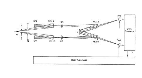
4 Th~ instrurnent is shown in Pig. 1, including the
optics and data converter, along with the host complll:er (in
6 block diagram format). Tlle source of optical radiation S, is
7 typically a deuterium or xenon lamæ for the UV region. A
8 tungsten-halogen lamp can be used if absorbance in the visible
9 region is desired. A cone of light shaped by an auerture, A1,
is reflected by front surface concave mirrors MClR and MClS, to
11 form a reference beam and a sample beam and focus each beam
12 respective].y onto a sample cell and a reference cell, both
13 equipped with optical windows. For HPLC applications, the
14 cells are low volume flow cells. Alternatively, the reference
cell may be replaced by a precision aperture.
1~ After passing through the cells, or Elow cells, each
17 beam is intercepted by front surfaced concave mirrors, MC2R and
18 MC2S onto a sinyle horizontally ruled grating which
19 respectively reflects and disperses the beams onto a pair of
matched photodiode arrays. The concave front surfaced mirrors
21 also focus the dispersed beams onto the respective photodiode
22 arrays. Each diode element, Ei, in the photodiode array
23 collects the light from the dispersed beam over a given
24 wavelength band, dLi. The range of wavelengths collected by
the photodiode array for a given angular position of the
26 yrating is the sum of the wavelength bands for each element in
27 the array.
28 The concave front surfaced mirrors, flat front
29 surfaced mirrors and grating are arranged so that for each
light beam, the angles between the incident beam and the
' '
'
'~ ~ " ,, ' ' ' ,
. , ,, , ~ ,. . '
1~ 132~a~1 ~
1 reflected beam are less than 20. In this manner, the
2 reference and sample bearns are maintained in a substantially
3 parallel formation and the light source, the sample and
4 reference cells and photodiode arrays can be isolated from one
S another in an essentially straight tunnel-like forrlu~tion. In a
6 preferred embodiment, the angles between the incident beam and
7 the reflected beams at the first pair of concave front surfaced
8 mirrors are about 12.4 and at the flat front surface mirrors
9 are about 11.5, and the angles between the incideslt beam and
reflected beams at the second pair of concave front surface
11 mirrors and the grating are both about 15.~.
12 Each wavelength element in the sample array, EiS, has
13 a corresponding wavelength element in the reference array,
14 EiR. The log of the ratio oE the voltage generated is
oroportional to the absorbance of the chemical compourlds in the
16 sample cell for the given wavelength band. The absorbance is
17 proportional to the concentration of the compounds in the
18 sample cell and thus can be used to quantitate the amount of
19 the chemical compound of interest. By comparing successive
elements in the two arrays, the absorbance as a function of the
21 wavelength can be generated.
22 By changing the tilt of the grating, a difeerent
23 wavelength range can be selected. A movable filter llolder may
24 interpose a filter into the beam between the source and the
first pair of concave front surfaced mirrors to eliminate
26 possible second order effects ;n the longer wavelenyth regions
27 (See F;g. 1). Another portion of the filter holder can be
28 positioned to block the beams for checking the dark current of
29 the arrays.
' ' ' s . ,
.
; ' ' ' - " .
~, `
13 2 ~ .) 01
1 ~ unique logarithmic data converter is desiqned for
2 use with the photodiode arrays. The non-linear data converter
3 is a type of ratiometric and logarithmic data converter with
4 simple circuitry that is economical to manufacture.
E'ig. 4 is a simpliEied version of the log converter
6 circuit for purposes of illustrating the beam intensity to
7 sample absorbance conversion concept. Fig. S showr; the timing
diagram Eor the converter circuit of Fig. 9. A sample signal
9 voltage, Vs~ and a reference signal voltage, Vr(O)~ each
corresponding to respective beam intensities at an identical
11 beam wavelength, are input to the data converter circuitry.
12 An ideal switch, S, is initially closed, bringing the
13 ¦ capacitor voltage to the desired initial voltage level,
14 ¦ VrtO). Then simultaneously, the switch is opened and the
timer is started. When the comparator senses that the
16 capacitor C voltage has decayed to the sample voltage, the
17 timer is stopped. The time interval, which is proportional to
18 sample absorbance is the output of the converter. The
19 conversion process then is repeated for additional pairs of
sample electrical signal and reference electrical signal inputs
21 from the photodiode array to generate a spectrum of sample
22 absorbance over many wavelengths. Once the photodiodes arrays
23 have been sampled to produce a rnultiwavelength spectrum, the
24 cycle may be repeated to provide a series of multiw~velength
spectra over time.
26 Refering to the timing chart of Fig. 5, which shows the
27 comparator input and output signals for one data conversion,
28 switch S, initially, is closed and Capacitor C, cha~ged to the
29 reference signal voltage level. As a result, the comparator
input V~ equals the reference signal voltage, while the
., . ~ 1 ' ' .
- ...
.. ' :, ~
: ~ .
-~
~ 3 2 ~
;~ 1 comparator input V, equals the sample signal voltage.
2 ~ecause the reference signal voltage is greater than the sample
3 signal voltage, the comparator output, V0, is in the state
4 for V, greater than V,.
At time, t3, switch S is opened and Capacitor C
6 discharges through resistor R. When the Capacitor C discharges
7 to the sample signal voltage level, the comparator output,
8 VOt flips triggering the timer to stop. This time is
9 designated t,. The time interval between to and tl is
T. The comparator input V,(t) is given by the Eor~nlla:
11
12 Vr(t~ = V,(O)e~'''' (1)
13
14 Transposing Eormula (1) yields:
16 ln [V,(0)/V,(t)] - (1/RC)t (2)
17 or log [V,(0)/V,(t)l - (ln 10/RC)t (3)
18
19 At the end of tirne interval T, V,(T) ~ V5
20 log [V,(0)/V,] ~ (ln 10/RC)T ~ kT (4)
21 where k ~ constant - ln 10/RC.
22 Rnowing that the absorbance is directly proportional to the
23 logarithrn of the ratio of the reference signal voltage to the
24 sampla signal voltage, log [Vr(0)/Vg], the time interval,
T, provides an indication of absorbance.
26 Fig. 6 represents a practical embodiment of the log
27 converter circuit to account for charge injection by switch S,
28 and input bias currents to the comparator. Fig. 7 is a timing
29 diagram for the circuit of Fig. 6. 8ecause solid state
switches tend to inject a small amount of charge when switched,
. . , ~, .
.
,
"' ' : ' ' ~. . , ' ~ ' ' :
I ~32~
1 a small shift in the initial capacitor voltage occurs at the
2 time the switch is opened. To account for the small shift an
3 additional switch S' is added in the sample signal voltaqe
4 path. As a result, the same shift will occur in both the
reference signal voltage path and the sample signal voltage
6 path. Pre~erably, S' and S are two elements of the same
7 monolithic integrated circuit. ilowever, ;t is only necessary
8 that the switches S and S' have substantially identical
9 parameters.
To account for input bias currents which lllay cause an
11 undesired error voltage to be generated on the RC net~ork,
12 identical impedances are provided at both input c~ulnnels to the
13 comparator. Thus, a resistor, R', and capacitor, (:', are added
14 to the sample signal voltage path. Preferably R' and C' are of
the same type and values as their counterparts R and C. The
16 connection for R' and C', however, varies from the connection
17 of R and C so that capacitor C' will not discharge.
18 The modifications added to the circuit of Fig. 6 cause
19 the switch charge injection and comparator bias cu~-rents to be
substantially equal at both input channels to the colllparator.
21 Thus the injection and bias currents are presented as
22 common-mode signals substantially eliminating any impact on the
23 comparator output.
24 With regard to the operation of the log converter
embodiment of Fig. 6, s~itches S and S- initially are closed
26 causing capacitor C to be charged to the reference signal
27 voltage level and capacitor C' to be charged to the sample
28 signal vcltage level. At time to ~ the switches are opened
29 and the timer begins to count. As with the circuit of Fig. 4,
the opening of switch S causes capacitor C to discharge through
~".~, , , . ., ;. ........... . .......... . .
~': ' ' ' -' '' ; ' . \, : ~ ., ', ".
': . ' :
~ - - ` ~
~ 3 ~
l resistor R. When capacitor C discharges to the sample signal
2 voltage level the comparator output flips triggering the timer
3 to stop. This tima is designated t, and the time interval
4 between to and tl is designated T. As with the circuit of
Fig. 4, the formula describing v,~T) is:
7 log [v,(0)/V,] - (ln 10/RC)T - kT
8 where ~ ~ constant - ln lO/RC.
The absorbance similarly is directly proportional to the tirne
11 interval, T.
12 Fig. 3 illustrates the photodiode array circuits and
13 the log converter circuit embodied to provide for
14 rnultiwavelength absorbance detection. Fig. 8 is a tirning
diagram for timinq signals S0 - S6.
16 After each of the dual beams impinge upon the flat
17 grating, each beam is diffracted into a multiwavelength
18 spectral beam. The multiwavelength spectral beam associated
19 with the sample source strikes the sample source photodiode
array, while the spectral beam associated with the reference
21 source strikes the reference source photodiode array. Each
22 photodiode array may include about 30-70 diodes, preferably 40,
23 most preferably 38 diodes. The light striking each diode is at
24 a specific wavelength different from the wavelength of the
light striking other diodes. Both the sample si~nal channel
26 and reference signal channel include a multiplexer for
27 selecting which photodiodes are to be read. The multiplexer
28 select lines for each channel correspond so that the photodiode
29 selected for the sample channel and the photodiode for the
reference channel are correspondin~ photodiodes which receive
.
, . ~
-~-\ l
:
.~ 1 light at the same wavelength from the respective beams. The
2 photodiodes in each array are read se~uentially, such that the
3 signal outputs from the photodiode arra~s are pipelined through
: 4 the data converter circuit in serial sequence. The sample
S signal goes through the sample ~ource channel, while the
6 corresponding reerence signal goes through the reference
7 channel. As illustrated, the host computer provides the line
~ select for determining the sequence of sampling the photodiode
9 arrays. However the line selects may be determined from
another source or automatically programmed to sequentially
11 access the diodes within the arrays.
12 The respective sample and reference signals go through
13 respective charge amplifiers to convert the signals to a signal
14 voltage. The voltage signals then pass through respective
charge conditioning circuits.
16 The charge conditioning circuits each include a
17 resistor network for summing to the sample voltage or reference
18 voltage, correction voltages to compensate ~or photodiode dark
current errors and multiplexer charge injection. The
correction voltages are inputted from the host computer to the
21 respective resister networks via a digital to analog
22 converter. The sample signal voltage and reference signal
23 voltage then enter respective sample and hold circuits. In one
24 embodiment, each o~ the sample and hold circuits includes a
multiple~er for selecting either the on-line sample signal
26 voltage and reference signal voltage or alternative calibration
27 signals which enable calculation of the correction voltages.
28 The input, M, originating at the host computer determines the
29 mode in which the sample and hold circuits operate.
. ~ , ' " "i ' ` ' ` ~ ' '
: ' ':
~!324~i01
l After being output from the sample and hoL(l circuits,
2 the sample signal voltage and reference signal voltage then
3 enter the data converter circuit. The data converter circuit
4 corresponds to the circuit as described for Fig. 6, although
5 ¦ the counter/latch corresponds to the timer of Fig. 6. The
6 count that is latched into the counter is proportional to the
7 sample absorption and is read and processed by the host
8 computer to be formatted, store~ and/or displayed.
9 The pipelining of sample and reference signals,
including the charge to voltage conversion, signal conditioning
11 and logarithmic conversions are controlled by the timing and
12 control circuit o~ Fig 3. The timing and control circuit may
13 be a PLA, ROM look-up table, discrete logic circuitry, CPU or
14 other circuitry capable of cyclically generating timing signals
~or the data conversion process. In the preferred embodiment
16 the timing signals include signals S~ through S6 as
17 illustrated in the timing diagram o~ Fig. 8. The tim;ng of the
18 Fig 3 circuit is illustrated in Fig. 8 by the timing signals
19 S0 to S~.
Referring to Fig. a, at point l, the system has been
2L idle awaiting to be triggerred by the host computer. The
22 system remains inactive for l clock pulse after the trigger.
23 At point 2, the sample and hold circuit is strobed,
24 via S2 ~ to acquire data from the signal conditioning
circuit. This signal is the charge amplifier output from the
26 ¦ discharged photodiode, modified by the dar~ current correction
27 supplied by the host comeuter during the previous c~cle.
28 At point 3, data from the previous conversion is
29 clocked fronl counters to data registers on the rising edge of
Sl. This signal also clears the counter and initiaLizes the
~ ' , . . .
'''.
.: ' ' '; ' ~ '' ': `
:.
132~SOl
l data converter capacitors, C' and C, for the ne~t conversion.
At point 4, the falling edge of S, starts the data
: 3 convertet action by opening the analog switches, S and S',
4 enabling the counters. ~he sample and hold circuits are put to
a ~hold" condition via Sz to provide a sustained signal to
6 data conversion.
At point 5, Ss is brought low to reset thc charge
8 amplifier so as to prepare for the next pair of siqnals Erom
9 the sample beam photodiode array and reference beam photodiode
array.
11 At point 6, signal S6 initiates a host computer
12 request for interrupt service, while signal Sq strobes the
13 multiplexer to load the line select and prepare Eor
14 transEerring the next sample signal and reference signal from
the respective photodiode arrays.
16 Sornetime between point 6 and the start of the next
17 cycle (at point l), the host computer will service the
18 interrupt and (l) read the data from the counter/latch, (2)
19 output the number of the next photodiodes to be selected to the
multiplexers, and (3) output the dark current corrections for
21 the next signals to enter the signal conditioning circuit.
22 ~ecause of the pipeline sequencing of photodiode array outputs,
23 the host computer deals with difEerent operations on the sample
24 signals and reference signals at once. For example, if sample
signal voltage (N) is currently being converted by the data
26 converter section, then the absorbance output (N-l) is being
27 read from the counter~latch, while dark current corrections are
28 being provided to the signal conditionin~ circuit Eor sample
29 signal voltage and reference signal voltage (N~l), and the
sample signal and reference signal ~N~l) are the slclnals about
, 1
,
,
:
- . , : ~ :
:
132~
1 to
be introcluced to tS~e charge amplifier. Additionally, the
2 hos
t computer is generating the line select signals for diode
num
bers for signals (N~2).
4 ~t point 7, the reset signal is removed from the
charge amplifier, and the system is allowed to remain idle for
6 a settling time.
7 At point a, the photodiode multiplexers ~re enabled to
8 transfer a sample signal and re~erence signal ~rom the
9 respective photodiodes to respective charge amplifiers.
At point 9, the rnultiplexer is disabled, ol~ening the
11 input circuit of the charge amplifier. The charge amplifier
12 output ~ill thus remain stable awaiting acceptance ~after
13 conditioning) by the sample and hold circuits on the next cycle.
14 At point lo, SO goes high, inhibiting data flo~
until the timing generator triggers the next cycle restarting
16 the timing sequence ~rom point 1.
17 The time scale on the timing diagram of Fig. 8 is in
18 clock periods of 10.24 microseconds. The complete flow
1~ sequence for a one wavelength conversion therefore takes
approximately 1.223 milliseconds. The interval between cycles
21 is normally 2.50 milliseconds, although the timing generator is
22 inhibited for approximately 1/2 this time. For appro~imately
23 40 diodes per photodiode array, the conversion for an entire
24 spectrum takes approximately 0.1 second. Because the sample
signal and reference signal outputs are pipelined through in
26 real time and are not simply a frozen snapshot of tSle
27 approxirnately 40 pairs of photodiode cSlarges, there is a slight
28 variation in time between the conversion for the signal at the
29 first wavelength and the conversion for the signal at the last
wavelength orf the spectrum. The absorbance outputs from the
~' .
~ - 20 -
, ~ :. .
. .
1324~01
1 counter/latch may be formatted by the host computer to generate
2 A three dimensional plot of sample absorbance vs. beam
3 wavelength over time.
4 The multichannel spectrophotometer of the present
invention tested over a period o~ time shows a high degree of
6 stability, drift of less than 2 X 10⁻⁴ AU/C or 2 X 10⁻⁴
7 AU~hour after warmup, a noise level of ~2 X 10 5 A[l in the
8 range of 210-280nm using a standard low volume flow cell in the
9 sample cell with standard flow conditions, and a spectral range
of 190--/00 nrn.
11 While preferred embodiments of the invention have been
12 illustrated and described, the invention is not intended to be
13 limited to the e~act embodiment illustrated. The scope of the
14 invention is intended to be determined by reference to the
claims and their equivalents interpreted in light of the prior
1~ art.
21
.
28
29
,: " . .. ..
~ . ' ;'' ~ . ' ,' ~ ,