Note: Descriptions are shown in the official language in which they were submitted.
1 324686
Twi~ted ~ire Ju~per 81eetrical Intereonneetor
TECHNICAL FIELD OF THE INVENTION
The present invention relates to the field of
electrical circuit connector6, ~nd more spec$fically to
both an apparatus and a method for intereonnecting ~tacks
of p~inted circuit boards.
BACRGROUND OF THE INVENTION
Integrated eireuits are typically fabrieated on
wafer~ which ~re then eut up to form individual integr~ted
eircuit~. The6e individual circuits are packaged within
hexmetically 6ealed eeramic or plastie paekages. The
6ignal and power lines from the integrated eireuit are
brought out to the pln~ of the paekage by means of leads
attached to bondinq pads on the integrated cireuit ehips.
The ehips are then used to form larger circuit~ by
interconnecting the integxated eircuit p~ckages by mean~ of
prlnted eireuit bo~rds. These eircuit boards may contain
several layers of electrical intereonnect. Typieally the
$ntegrated cireuit paekages are aoldered to the eireuit
board. The solder$ng process forms an elecitrical and
mechanical connection batween the integr~ted circuit
package and the circuit board.
To form still larger eireuit6 called modules,
circuit boaxds may be arranged and interconnected in a
variety of ways. One popular high density interconnect
scheme is to stack the circuit boards in a sandwiched
relationship and electrieally interconnect the eircuit
-" I 324686
boards with ~umpers passed through the stack ~long the Z
axi~. Thi6 packing ~cheme ~chieves a relatively hiqh
packing den ity ~imited by heat di6~ipation ~nd connector
spacin~ requirements.
S The aforementioned technique of forming larger
circuit6 by u6ing individually pack~ged integrated circuits
mounted on circuit board~ limits packing density. The
actual integrated circuit chip~ themselve~ are typlcally
smaller than one-tenth of a ~guare inch, and only cover
only 10-20 percent of the board area. Due to the low
density achieved through the use of individually packaged
integrated circuit chips and traditional interconnection
technology, it is difficult to increase the operating speed
of the system. Additionally, the inter-board spacing of
~tacked circuit boards is limited by the height of the
integrated circuit packages ~nd the inter-board connects.
This limits packing den~ity in the z direction ~8 well.
Configuratlons which li~it packing density limit the
interboard signal speed due to the long propagation delays
~seociated with the long interconnect lines.
Another problem presented by traditional
configurations relates to the ease with which modules csn
be disassembled. Forms of construction which involve
soldering and ~taking of the board assemblies typicall~
re~ult in modules which cannot be disassembled or repaired.
The present invention provides ~ new apparatu~ and
method for high-density interconnects of circuit boards
which overcomes these disadvantages of the prior art.
SUMNARY OF THE INVENTION
The present invention provides for the
interconnection of sandwiched circuit board~ through the
use of twisted wire ~umper connectors installed in
interconnection apertures of circuit boards.
The circuit boards disclo~ed for use with this
1 324686
invention have the integr~ted circuit chips attached
directly to the printed circuit without the tradit~onal
ceramic or plastic packaging. ~he circuit boards them~elves
are manufactured with plated- through hole~, having hole
S patterns 6ubstantially matching the bonding pad patterns of
the integrated circuit chips.
The integrated circuit ch~ps are manufactured with
flying leads which are positioned facing the circuit board.
The flying leads are ~nserted through the plated holes so
that the flying leads protrude from the circuit board.
Caul plates are then poRitioned on the outer sides of this
sandwich and pressed together ~o that the 6ticky or soft
gold of the flying leads is compres~ed within the pl~ted
holes, causing the soft gold to deform against the 6urface
of the plated holes and thereby forming a strong electrical
and mechanical bond. The caul pl~tes are then removed and
the integrated circuit package remains firmly attached to
the circuit board. Thi~ results in improved packing
density of integrated circuit chip~ on circuit boards.
Two or more ~tacked circu$t bohrds are interconnected
using electrically conductive tw$sted wire ~umper
connectors or ~umpers inserted into the plated-through
hole~ of the stacked circuit boards. The twisted wire
~umper connectors are made from multi-filament wire and
have enlarged portions called bird cages, formed along
their length. Thes~e bird cages bow out to a large outer
radius, which ~ larger than the inner radius of the
plated-through holes of the printed circuit boards. The
twi~ted wire ~umper connectors are used as inter board
~umpers for the tran~mis6ion of power or logic 6ignals. The
~umpers are preferably drawn through the stacked circuit
board~ through the use of a leader. The wiping action of
the insertion create~ ~ low impedance electrical connection
between the circuit bosrd~. The twisted wire ~umper
connector is made slightly longer than the stack height of
- 1 324686
the module 80 that a portion of the twisted wire ~umper
connector protrude6 through one or both side6 of the
~andwich of circuit boards forming a ~tub. This stub may
then be used to a6Ri6t in the removal of the twi~ted wire
jumpers to facilitate module repair.
Thus in connection with thi6 divisional
specification the present invention provides a twisted
wire jumper for interconnecting electronic assemblies
comprising:
a plurality of cylindrical portions, each comprising;
a central core strand;
a helically wound, multiple 6trand coil sheath
surrounding said central core strand; and
a plurality of connector portions, each comprising;
a plurality of resilient strandc forming a barrel
shaped cage for connection with said electronic assemblies.
In another a6pect the invention provides a
twisted wire jumper for interconnecting electronic
assemblies having interconnection apertures comprising:
a central core strand;
multi-fil~ment coil strands ~urrounding said core
strand, forming a plurality of bulged cages for resilient
frictional engagement of ~aid interconnection
apertures,providing electrical interconnection and
releasable mechanical connection between said assemblies.
- ` 1 324686
-
In a further a~pect the invention provides
a twisted wire jumper for interconnecting
electronic a~emblie~, which hAve ~nt~rconnection
apertures, compri~ing:
a central core strand having ~ head portion ~nd having
a tail portion;
a helically oriented coil ~urrounding said core ~trand,
wound to form a 6equence of bulged cages for
resilient frictional engagement of sa$d interconnection
apertures, providing electrlcsl interconne~tion and
rele~sable mechanical connection between said
assemblie~,and
wound to form a seguence of cylindric~l sections
for the electrical coupling o$ said bulged cage6 and for
the mechanical support of said bulged cages.
In another embodiment this divisional
specification provides a method of manufacturing a
twisted wire jumper contact comprising the steps of:
clamping a wire to place it under tension;
melting said wire to form a blunt nose;
crimping said wire at first and ~econd locations to form
a pair of crimp collars;
rotating said wire in an anti-helical direction to form a
bulged cage section between said collars;
releasing sa~d wire;
advancing said wire to form a cylindrical section.
In still another embodiment this invention
provides an elongated ~umper for interconnecting a
plurality of electronic assemblies, comprising a
plurality of cylindrical portions and a plurality of
connector portions separated by a cylindrical portion
along the length of the ~umper, wherein:
-4a-
1 324686
each of the plurality of cylindrical portions comprises:
a central core strand;
a helically wound, multiple strand coil sheath
surrounding said central core strand; and
each of the plurality of connector portions comprise~:
a plurality of resilient strands forming a barrel
shaped cage extending transversely outward a greater distance
than the sheath of an adjacent cylindrical portion, the barrel
shaped cage adapted for connection with said electronic
assemblies.
In still a further embodiment the invention
provides a method of manufacturing an elongated twisted
wire jumper from a wire formed by a plurality of
helically wound strands, compri~ing the steps of:
clamping said wire to place it under tension:
melting said wire to form a blunt nose;
crimping said wire at first and second locations to form a
pair of crimp collars;
rotating said wire in an antihelical direction to form a
bulged cage section between said collars;
releasing said wire;
advancing said wire to form a cylindrical section.
~RIEF DESCRIPTION OF THE DRAWINGS
In the drawings like numerals $dentify like
components throughout the several views.
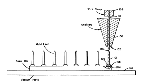
FIG. 1 i~ a side view of an integrated circuit
die onto which flying gold leads are ball bonded and
6traightened by a ball bonding machine.j
FIG. 2 8hows the ~ix step6 that the flying lead
ball bonder performs in order to attach a flying lead to an
integrated circuit die.
FIG. 3A show6 the bonding pad pattern on a typical
integrated circuit.
FIG. 3B ~hows the corresponding plated-through
hole pattern on a circuit board which mates the integrated
circuit chip onto the circuit board.
-4b-
1 324686
FIG. 4 shows the relative positions of the
integrated circuit chip and the circuit board prior to
compression of the flying leads into the plated holes.
FIG. 4A is a closeup view of the relative
positions of the integrated circuit chip and the circuit
board prior to compression of the flying leads into the
plated holes.
FIG. S ~hows the relative positions of the
integrated circuit chip and the circuit board after the
flying leads have been compressed inside the plated holes
of the circuit board.
FIG. 5A i8 a closeup view of a ball-bonded flying
lead that has been compressed into a plated-throuqh hole on
the circuit board.
FIG. 6 is a ~ide view of the compression process
~4c-
1 324686
wherein a plurality of integrated circuit chip~ hav~ng
flying leads ~re att~ched to ~ sin~le printed circult board
through the application of ~eating force on c~ul plates
which sandwich the circuit board/chip combination.
FIG. 7 shows a plated-through hole pattern for a
typical board onto which integrated circuit dice are
nttached in the preferred embodiment of the present
invention.
FIG. 8 ~hows a module ~ssembly having a plurality
of circuit b~ards nested together.
FIG. 9 is a side view of the module assembly of
Fig. 8 showing the det~ils of the logic ~umpers and power
~umpers for logic and power interconnection between the
stacked ~andwich a~sembly of printed circuit boards.
FIG. lOa shows the twisted wire ~umper logic
~umper or connector.
FIG. lOb 6hows the twisted wire ~umper power
~umper or connector.
FIG. lOc depicts a cross section of the wire used
to form a twi~ted wire ~umper connector.
FIG. lOd depicts a cross ~ection of a bird cage
formed in a twisted wire ~umper connector.
FIG. lOe shows a cross section of a crimp in
the wire.
FIG. 11 shows a cross-sectional view of ~ single
twisted wire ~umper logic ~umper that has been installed
through axially aligned plated-through holes of a st~ck of
printed circuit boards of the module assembly of Fig. 9.
The f$gure is 8hown in an exaggerated scale to clarify the
operation of the invention.
FIG. 12 iS acros~-section~l view of a single
twisted wire ~umper power ~umper that has been installed
through the axially aligned plated-through holes of the
~tacked~array of printed circuit boards of the module
1 324~86
as6embly of Fig. 9. The figure i~ ~hown in ~n exaggerated
scale to clarify the operation of the ~nvent~on.
FIG. 13 is a 6ide view of mechanical 6chematic
which ha6 been greatly exagger~t~d to show a 6ingle
S twi6ted wire jumper compensating for the mi6alignment of
a ~tack of printed circuit boards.
FIG. 14 6how6 ~ method for in~talling twi~ted w~re
~umper connectors into a stack assembly of four printed
circuit boards.
FIG. 15 6how~ the method of manufacturing twi6ted
wire ~umper connectors.
FIG. 16a showE an slternate form of a twi~ted wire
~umper.
FIG. 16b 6hows a cross ~ection of the twisted
wire jumper shown in FIG. 16a.
FIG. 16c shows a cross section of the twisted
wire jumper shown in FIG. 16a.
DETAILED DESCRIPTION OF THE
PREFERRED EMBODINE_
The preferred embodiment of the present invention
involves the high-density packing of 6ilicon or
gallium srsenide (GaAs) integrated circuit chips onto
~ingle-layer or multi-lsyer interconnect printed circuit
bosrds. The circuit boards have plated-through holes or
interconnection apertures which permit the hiqh-density
packing of circuit bosrds in a sandwiched arrangement. The
application of this technology permits improved speed,
improved hest dissipation, and improved packing density
required for modern ~upercomputers such ~s the Cray-3
manufactured by the as6ignee of the present invention.
'
1 324686
In the preferred embodiment of this application,
the integrated c$rcuit chips are att~ched to the circuit
board by flying yold leads, ~8 discussed below and
disclosed in Canadian application Serial No. 567,0a4
5 which i6 ~s~igned to the 6ame assignee of the present
invention. By placing the integrated circuits directly
on the circuit, the bulky packaging normally found on
inteqrated circuit~ is elimina~ed.
Fl~inq Lead Construction
FIG. 1 ~hows the preferred embodiment for
attaching the flying gold leads to the 6ilicon or gallium
arsenide packaged chip or die before attachinq the die to
the circuit board. The leads ar0 made of soft gold wire
which is approximately 3 mil6 in diameter. The GaA~ chips
u~ed in the preferred embodiment contain 52 bonding pads
which have a sputtered soft gold finish. The ob~ective of
the die bonding operation is to form a gold-to-gold bond
between the wire and the pad. A Hughes automatic
thermosonic (gold wire) ball bonding machine Model 2460-II
may be modified to perform this operation. Thi~ machine is
available from Hughes ~ool Company, Los Angeles,
California. This machine wa8 designQd and normally used to
make pad-to-lead frame connections in IC packages and ha~
been modified to perform the step~ of flying lead bonding
a~ described below. The modifications include hardware and
software changes to allow feeding, flaming off, bonding and
breaking heavy gauge gold bonding wire (up to 0.0030 dia.
Au wire).
The Hughe~ automatic b~ll bonding machine ha~ an
X-Y positioning bed which is used to posltion the die for
bonding. The die is loaded on the bed in a heated ~acuum
fixture which holds up to 16 dice. The Hughes bonding
machine i~ aquipped with a vi~ion system which can
1 324686
recognize the die patterns without human intervention and
position each bonding pad for proce~slng.
The soft gold wire thst i~ used for the flying
leads in the preferred embodiment of the pre~ent invention
S is sometimes referred to ~s sticky gold or tacky gold.
This gold bonding wire i~ formed from a 99.994 high-purity
~nnealed gold. The process of annealing the h$gh-purity
gold results in a high elongation (20-25~ ~tabilized and
~nnealed)~ low tensile strength (3.0 mil., 50 gm. min.)
gold wire which is dead ~oft. The wire composition (99.99%
pure Au non-Beryllium doped) i~ ns follows:
Gold 99.990% min.
Beryllium O.002% max.
Copper 0.004% max.
Other Impurities (each) 0.0034 max.
Total All Impurities 0.010% max.
This type of gold i8 available from Hydrostatics (HTX
grade) or equivalent.
Referring to FIG. l, the flying lead die bonding
procedure begins with the formation of a soft gold ball 106
at the tip of the gold wire 101. The wire i8 fed from a
supply spool (not shown) through a nitrogen-filled tube lO9
(shown in FIG. 2) to a ceramic capillary 100. The inside of
the capillary is ~st 61ightly l~rger than the wire
di~meter. The direction of nitrogen flow in the connecting
tube 109 can be altered to drive the wire either toward the
die or toward the supply spool. Thi~ allows the gold wire
to be fed into or withdrawn from the capillary t$p.
The gold ball 106 formed at the end of the gold
wire 101 i6 thermo60nically bonded to bonding pad 105 of
chip 104. The capillary tip 102 of capillary 100 is
capable of heat$ng the ball bond to 300C concurrent with
pressing the ball 106 onto the pad 105 and ~onically
1 3246~6
vibrating the connection until a etrong electrical snd
mechanical connection i8 formed. The cspillary 100 $8 then
withdrawn from th0 ~urface of the die 104 and tho wire 101
is extruded from the tip 102. A notching mechanism, added
to the Hughes ball bonder to perform the specific notching
operation described herein, i5 used to make ~ notch 107 at
the appropriste height, thus defining the length of the
flying lead. The wire clsmp lOB grasps the gold wire 101
~nd the capillary i8 withdrawn upward, breaking the flying
lead at 107 ~nd concurrently performing a nondestructive
test of the ball bond to bonding pad connection and slso
straightening and stiffening the flying lead.
The sequence of steps required to make a flying
lead bond to the package die i6 6hown in FIG. 2. Step 1
begins with the feeding of a predetermined amount of wire
through the capillary 100. A mechan~cal arm then po~itions
an electrode 114 below the capillary tip 102 and a
high-voltage electrical current forms an arc which melt6
the wire and forms a gold ball with a
diameter of approximately 6 mils. This operation is called
electrostatic flame-off (EFO). Ball size is controlled
through ad~ustment of the EFO power supply output. During
this step, the cl~mp8 108 are closed and the nitrogen drag
is off. This action occurs above the surface of the
integr~ted circuit chip BO ns to avoid any damage to the
chip during the EFO ball forming process.
In step 2, the nitrogen drag 109 withdraws the
supply wire 101 into the capillary 100 and tightens the
ball against the capillary t$p 102.
The capillary tip 102 is heated to approximately
200C to assist in keeping the gold wire 101 in a
malleable state. The die fixture is also heated to 200C
to avoid wire cooling during the bonding process. The die
fixture i8 made of Teflon*-coated aluminum. Teflon is
a trademark for polytetrafluoroethylene. As shown in
*Trademark 9
- I 324686
FIG. 1, a vacuum cavity or vacuum plate 103 hold5 the die
104 in position on the fixture during the bondin~ process.
In ~tep 3, ~he bonding mschine lower~ the
capillary 100 to the surface 105 of a bonding pad and
applies high pre6sure (range of 30-250 gram~) to the
trapped gold ball 106 along with ultraqonic vibration at
the capillary tip 102. The capillary t$p 102 i3 flat, with
a 4-mil inside diameter and an B-mil out~ide diameter. ~he
ball 106 i6 flattened to about a 3-mil height and a 6-mil
di meter. ~ltra~onic energy is supplied through the
ceramic capillary 100 to vibrate the gold ball 106 and
scrub the bonding pad surface. The sound i8 oriented 80
that the gold ball 106 moves psrallel to the die ~urface.
The Hughes ball bonding machine has the ability to vary the
touch-down velocity, i.e., soft touch-down for bonding
GaAs, which i8 program selected. The ultrasonic
application is also program selected.
In step 4, the capillary 100 is withdrawn from the
surface of the die 104, extending the gold wire 101 as the head is
raised. The nitrogen drag is left off and the capillary is
raised to a height to allow enough gold wire to form the
flying lead, a tail length for the next flying lead, and a
~mall amount of clearance between the tail length and the
capillary tip 102. The Hughes ball bonder device is
capable of sQlecting the height that the capillary tip can
move up to a height of approximately 0.750 inch.
In 6tep 5, ~n automatic notching m~chanism 115
moves into the area of the extended qold wire 101 and
strikes both sides of the wire with steel blades. This is
e~sentially n scis~or action which cuts most of the way
through the gold wire 101, forming a notch 107 (F~G 1). me notch
107 is made 27 mils above the surface of the die The
notching mechanism has been added to the Hughes ball bonder
for the precise termination of the flying leads. The
Hughes ball bonder has been modified to measure and display
~ 32~686
the notch mechanism height. The activation signal for the
notch mechanism iB provided by the Hughes ball bonder
system for the proper activation during the sequence of
ball bonding. The flying lead length i8 ad~ustable from
between 0.0 mils to 50.0 mil6. It will be appreciated by
those 6killed in the art that the notching function can be
accomplished with a variety of ~echani~ms 6uch as the scissor
mechanism di6closed above, a hammer-anvil system, and a
variety of other mechanisms that merely notch or completeiy
sever the wire 101.
In step 6, clamp 108 closes on the gold wire 101
above the capillary 100 and the head i~ withdrawn until the
gold wire breaks st the notched point. This 6tretching
process ~erves several useful purposes. Primarily, the gold
wire is straightened by the stretching force and stands
perpendicular to the die 6urface. In addition, the bond is
non-destructively pull-tested for adhe~ion at the bonding
pad. The lead 101 is terminated at a 27-mil height above
the die ~urface 104 in the preferred embodiment. At the
end of step 6, the capillary head for the bonding mechanism
is positioned over a new bonding pad and the process of
steps 1-6 begins again. The bonding wire 101 is partially
retracted into the capillary once again, and the clamps are
closed, as shown in 6tep 1, 60 that a new ball may be
formed by the EF0.
The die positions are roughly determined by the
loading po~itions in the vacuum fixture. The Hughes
automatic bonding mschine is able to ad~ust the X-Y table
for proper bonding position of the individual die. An
angular correction i~ automaticnlly made to ad~ust for
tolerance in placing the die in the vacuum fixture. This
i8 done through a v$sion sy~tem which recognizes the die
pad configurations. Using the modified Hughe~ automatic
bonding machine with the current bonding technique, a
minimum bonding rate of 2 die pads per ~econd is possible.
11
1 324686
Circuf t Board Con~truction
Once the gold bonding leads are attached to the
inte~rated circuit chip or die, the die 18 ready to be
~ttached to the circuit board. As shown in FIG. 3A, the
bonding pattern of the integrated circuit die 104 matchec
the plated hole pattern on the circuit board 110,~hown in
FIG.3B. For example, the top view of integrated circuit
die 104 in FIG. 3A shows the bonding pad 105 in the upper
right corner. The circuit board 110 shown in FIG. 3B shows
a corresponding plated hole 111 which i6 aligned to receive
the b~ng lead ~rcm box~ng pad lO5 (shcwn in FIG. 3A) when circuit b~
110 is placed over integr~ted circuit 104 and the flying
leads are inserted into the hole pattern on the circuit
board. Thus, each bonding pad of integrsted circuit 104
has a corresponding plated hole on circuit board 110
aligned to receive the flying leads.
The circuit board assQmbly operation begins with
the insertion of the die into the circuit board. The
circuit board is held in a vacuum fixture during the inser-
tion process to make sure that the board remains flat.
Insertion can be done by hend under ~ binocular microscope
or production assembly can be done with a pick-and-place
machine.
Referring to FIG. 4, the circuit board 110 with
the loo~ely placed~diQ 104 is mounted on an ~luminum vacuum
caul plate (lower c~ul plate) 113. Steel guide pins (not
shown) are placed in corner holQs of the circult board to
prevent board motion during the assembly operation. A
second (upper) caul plate 112 is then pl~ced on the top
~ide of the circuit board populated with chips to press
again~t the tops (non-pad side) of the chips 104. The
sandwich assembly comprising the circuit board, the chip
and the c~ul plates i8 then placed in a press and pressure
1 324686
i6 applied to buckle and expand the gold le~ds 101 in the
plated hole~ 111 of the circuit board.
The 6ide v~ew of the sandwiched circuit board 110,
integrated circuit chip 104, ~nd c~ul pl~tes 112 ~nd 113 in
FIGS. 4 and 5 illustrates the position of the gold leads
101 before and after the pressing operation, respectively.
In the preferred embodiment there iB a 9-mil exposure of
gold lead 101 of a total lead length of 29 mil~ which upon
compression will buckle and expand into the plated hole 111
of the circuit board 110. The 3-mil diameter wire 101 in a
5-mil diameter hole 111 means the initial fill i~ 36
percent of the available volume. After pressing, the fill
ha6 increased to 57 percent as a result of the 9.2-mil
shortening of the gold lead 101. As shown in greater
detail in FIGS. 4a and Sa, the lead typically buckles in
two or more places, and these corners are driven into the
sides of the plated hole 111 of the circuit board. The
integrated circuit pad 105 i8 electrically connected to the
flying lead by the ball bonding proce~s. The flying wire
also electrically connects the integr~ted circuit to the
circuit board through the pressing operation.
The circuit board 110 may be removed from the press with
the integrated circuit chip 104 securely attached and
electrically bonded to the plated holes of the circuit
board.
FIG. 6 sh,ows a view of the circuit board press
which is used to attach the integrated circuits to the
printed circuit board. The upper caul plate 112 iB a
Teflon-coated seating c~ul plate which iB aligned through
alignment pins 114 with the circuit board 110 and the lower
caul plate 113 which is a vacuum caul plate to hold the
circu~t board flat during the pressing procQss. The
alignment pins 114 are used to prevent the printed circuit
board 110 from ~liding or otherwise moving during the
pressing process. A seating force is ~pplied to the top of
13
1 324686
upper caul pl~te 112 which forces the excess flying lead
material into the plated holes of printed circuit board
110. Thus, integrated circuits 104 are mechanically and
electrically bonded to printed circuit board 110.
It will be ~ppreciated by tho~e ~kill~d ln the art
that many variations of the above-described pressing
operation can be used which results in the ~me or
oquivalent connection of the flying lead~ to the circuit
boards. For example, the flying leads of the chips could
be completely in~erted into the through-plated holes of the
circuit board prior to the pressing operation with the
excass gold leads p~otruding out the opposlte ide. The
first caul plate could then be used to hold the chip onto
the circuit board while the second c~ul plate is used to
compress the leads into the holes.
Module AssemblY Construction
FIG. 7 shows an ex~mple of a printed circuit board
hole pattern for the circuit boards u6ed in the Cray-3
computer manufactured by the assignee of the present
invention. In the preferred embodiment of the present
invention, each circuit board provides 16 patterns of
plated-through hole~ for receiving the flying leads of 16
integrated circuits. The 16 integrated circuits are
~tt~ched to the circuit board ~hown ~n FIG. ? through the
pre~sing process previously described. Each aperture
pattern on the circuit board 110 corresponds to the
contact pad pattern shown on FIG. 3, from which the
bonded flying leads extend outward as shown in FIG. 4.
Each corner of circuit board 110 has a group bf four
plated-through holes 304 which are used for alignment
during initial assembly. These apertures 304 are also
used for power distribution in the completed module.
In the preferred embodiment of the present
invention, 16 circuit boards 110 of the type shown in
FIG. 7 are stacked together to form a module assembly 200 as
14
- 1 3246~6
shown in both FIG. 8 and FIG. 9. The circuit boards 110
~re arranged in n 4 x 4 matrix on each of four layers,
creating an X-Y-Z matrix of 4 x 4 x 4 circuit board~.
Therefore, each module assembly 200 has 64 circuit boards
containing 16 integrated circuit chips each, ~iving a total
of 1,024 integrated circuit chips per module assembly.
In the preferred embodiment, the module assembly
200 is 4.76 inches wide, 4.22 inches long, ~nd 0.244 inch
thick. As is shown in FIG. 8, ~t one edge of the module
sssembly are four machined metsl power blade~ 201a-201d.
These power blades are used both for mechanical connection
to the cabinet into which the module as6emblies are placed
~nd for electrical connection to the system power ~upplies.
At the opposite side of the module assembly are 8 edge
connectors 202a-202h used to communicate with other
modules. These connectors form the communication paths to
the other module assemblies within the machine. The
bundles of wires between the circuit boards of the module
s6sembly 200 and the board edge connectors 202a-202h ~re
2U provided with strain relief member~ 240a-240h respectively.
Each strain relief is a plastic member which protrudes from
the edge of the circuit boards. The interconnected wires
pass through holes in the strain relief members between the
circuit boards and the floating connectors 202a-202h. In
this fashion, the flexing of the wlres during the
connection and disconnection of connectors 202a-202h does
not strain the soldered connection of the wires to the
circuit boards. The strain relief members 240a-240h also
serve a~ spacers between the circuit boards in a fashion
s$milar to spacer6 203 described below. I
Electrical communication between the integrated
circuit chips of each board 110 is accomplished by means of
the prefabricated foil patterns on the surface and buried
within each circuit board. The electrical communication
between circuit boards 110 in the X-Y plane is by means of
1 324686
twisted wire jumpers 231 and 232 along the Z-axis
(perpendicular to the planar surface of the circuit boards
and the module assembly) effecting electrical connection
between the circuit boards llO, two logic plates 216 and
217 sandwiched in the center of the module assembly 200
and a centrally located power distribution board 210
sandwiched between the logic plates, as shown in FIG. 9.
The z-axis twisted wire ~umper6 231 and 232 may be used for electrical
communication signals and for power distribution. The Z-
axis ~umpers may be placed in any of the area on circuitboards 110 that is not occupied by an integrated circuit.
In the preferred embodiment of the assembly module,
anywhere from 200-1000 z-axis logic ~umper8 231 may be used for
a single circuit board stack. 6400-11,000 ~umpers may be
used for a module 200.
FIG. 9 shows a sectional view of a module
assembly 200. In the preferred embodiment, module assembly
200 is constructed as a sandwich of a electronic
assemblies. These assemblies include a plurality of
populated circuit boards 212,214,219,221,which are spaced
apart from each other using insulated spacers, such as the
one illustrated at 203. Another example of electronic
assemblies are the logic plates 216 and 217 which are in
contact with and are axially aligned with a power plate
210. All of the circuit boards are orientated 80 that the
flying leads of the integrated circuits 104 are away from
the power plate 2L0. Also as shown in FIG. 9, power blade
201 abuts circuit boards 212, 214, 219, 221 and logic
plates 216 and 217. Additionally, power plate 210 extends
into power blade 201. FIG. 9 shows all ma~or component6 of
a completely assembled module assembly 200 with the
exception of the edge connectors which have been omitted
for clarity.
All the electronic assemblies including the
circuit boards and the logic plates 216 and 217 are
designed 80 that when they are assembled into a module,
16
1 32~686
their plated-through holes become subQt~ntially aligned in
the Z-axis, with the complimentary plated-through holes of
the other circuit boards and logic plates.
The power plate 210 i~ designQd ~o that when it iR
~ssembled into a module, its larger unplated holes
~ubstantially align in the Z axis with the plated-through
holes of the circuit boards and logic plates. Likewise,
circuit boards 110 and power plates 210 sre designed so
that when assembled in a module a~embly, their plated-
through holes 304 become substantially aligned in the Z-
axis with corresponding plated-through holes on other
circuit boards and power plates.
However, logic plates 216 and 217 are designed so
that when they are a~sembled into a module, their plated-
through holes are sub~tantially aligned in the Z axi~ withthe plated-through holes 304 of the circuit boards and
power plate.
Electrical communication between the integrated
circuit chips on each board is accomplished in the X-Y
plane by means of prefabricated foil patterns on the
surface of, and buried within, each circuit board.
Electrical communication between circuit boards 21~, 214,
219, 221 is routed via foil patterns buried within logic
plate~ 216 and 217. Electrical inter-connect~ between
circuit board~ 212, 214, 219, 221 and logic plates 216 and
217 are accomplished by inserted electrically conductive Z-
nxis twisted wire ~umper log$c ~umpers 231 contacting logic
plate interconnection apertures 303 on the circuit boards
and logic plates.
As de~cribed in more detail below, the twisted
wire ~umper logic ~umpers or connectors have wire bird-cage,
or bulged portions that have a greater outer radius than
the inner radius, or inner contact surface, of the
complementary interconnection apertures shown as plated-
through holes 303. When a twist-pin logic jumper 231
is inserted into the module assembly, the wire bird-
17
1 324686
cage portions compress against the plated-through holes 303
thereby forming low resistance connections.
Electrical power di~tribution to the integrated
circuit chips on each board 110 i~ accomplished by means of
prefabricated foil pattern~ on the surface of, and buried
within, each circuit board 110. Electrical power is
di~tributed to circuit board~ 212, 214, 219, 221 through
power plate 210 which connects to each of the power blades
201a-201d. Electrical powex inter-connections between
circuit boards 212, 214, 219, 221 and power plate 210 are
accomplished by inserted Z-axis twisted wire ~umper power
jumpers or connectors 232. As described in more detail
below, the twisted wire jumper power jumpers also have
bulged portions, or wire bird-cages that, when compressed,
have a greater outer radius than the inner radius, or
inner contact surface, of the interconnection apertures
represented by plated-through holes 304. When a twist-pin
power jumper 232 is inserted in the module assembly, the
wire bird-cages compress against the plated-through holes
304 thereby forming low impedance connections.
In the preferred embodiment, module assembly 200 i8
stacked with other module assemblies in a fluid cooling
tank and po~itioned ~o that the planar surfaces of the
module assembly are stacked vertically. Thus, in the
preferred embodiment, FIG. 9 i8 a top-down look at module
assembly 200. A type of cooling apparatus suitable for
cooling the circuit board module assemblies of the present
invention i8 described in V. S. Patent No.i4,590,538.
Cooling channels 230, a8 shown in FIG. 9, are
provided to allow the cooling fluid to rise through the
module assembly to remove the heat produced by the
integrated circuits 104. Heat transfer occurs between
circuit boards 1 through 4 (levels 212, 214, 219, and 221
18
1 324686
respectively) and the cooling fluid in channels 230.
Cooling channels 230 are created by spacing the circuit
boards populated with integrated circuit~ 104 from one
another and from the logic plates using the above mentioned
insulated spacer6 203. The insulated spacers 203 are held
in place by twisted wire ~umper power ~umpers 232 during
module assembly.
Twist-Pin Connectors
FIG. lOa ~hows a single logic twisted wire ~umper
connector for coupling logic level signals between the
various electronic assemblies. The preferred embodiment of
the twisted wire ~umper shown in FI;G. lOa includes a
leader section 260, and a cylindrical tail section
261. Six bird cages 300 are formed between the
crimps shown on logic jumper 231. It is preferred
to weld the ends of the twisted wire jumper to form
blunt nose sections as shown by weld 306. The
leader 260 and the tail 261 may beyond the module
assembly after insertion to assist in both
installation of the twisted wire jumper connector
and its removal during module disassembly. At each
end of the connector a laser weld 306 is used to
keep the wires making up the twisted wire jumper
connector 231 from unravelling. The crimps 302 are
used to form the wire bird cages 300. The crimps
302 and cages 300 are spaced along the twisted wire
jumper to match the interboard spacing. It has
proved desirable to extend the cages beyond the
edges of the plated-through apertures in the printed
circuit boards. For the Cray-3 product this has
resulted in .028 inch crimp spacing. The 8iX bird
cages 300 are made as described below.
Refer to FIG. lOc. The preferred embodiment the
logic twisted wire ~umper 231 is m~de from seven strand
multi-filament Be/Cu wire tempered to either 1/4 or 1/2
hard. It is preferred to u~e w~re with uniform ~trand
diameters of approximately l.S to 1.6 mils in diameter. It
--19--
---` 1 324686
iB al80 preferred to use a nickel flashed, 30 microinch
gold plated, beryllium copper alloy 25 CDA wire available
from California Fine Wire Co.and other vendors. The ~even
strands ~re configured ~ a ~ix around one helix. The wire
diameter i8 approximately 4.8 mils before the bird cages 300
~re formed. Refer to FIG. lOd. The bird cages 300 bulge outw~d
to an outer radius of approximately 8.0 mils.
Refer to FIG. lOe. In the preferred embodiment,
the individual ~trands making up the wire are fused
toyether during the crimping operation.
FIG lOb show6 a ~ingle power twisted wire ~umper
connector for coupling power to the various electronic
assemblies. In the preferred embodiment the power twist- -
pin ~umper has a leader section 262, a tail ~ection 263,
~n~ a n~t~r of crimp6 302 fon~ug five wire bind cages 301. The
leader 262 and tail 263 may extend beyond the module
a66embly to assist in installation and remov~l of the
twi~ted wire ~umper connector. At each end of the connector
there i6 a weld 307 to keep the wires making up the twisted
wire ~umper connector from unraveling.
The 5 bird cages 301 are ~paced 60 that each bird
cage substantially aligns with a corresponding power
plated-through hole 304 of the module assembly 200.
Refer now to FIG. lOc. In the preferred embodiment the
power twisted wire ~umper 232 i8 made from seven 6trands of
either 1/4 or 1/2 ~ard, .0048 mil diameter, nickel flashed,
30 microlnch gold plated, beryllium copper alloy 25 CD~
wire. Ihe multi-fil~t wire is wo~d six an~d one (FIG. lOc) in a
left handed helix. At pre~ent the preferred wrap i8 30
turn~ per inch. The wire diameter i8 approximately 14.4
mils before the bird cages sre formed~ Refer now to FIG.
lOd. The bird cages bulge outward to an outer radius of
approximately 16.0 mils.
~ 20
- 1 324686
Refer to FIG. lOe. In the preforred embodiment,
the individual ~trand~ making up the wire are fused
together during the crimping operation.
FIG. 11 show6 a cut-away view of a single logic
5 twisted wire ~umper in~talled in a module a~embly. The
bird cages 300 compress again~t the plated-through holes
303 forming low impedance electrical connections. The
leader 260 ~nd tail 261 extend beyond the module a~sembly
to assi6t in module disassembly. Also ~hown are conductive
paths 400 connected to circuit boards 212, 214, 219, and
221 for logic level routings to integrated circuit6 104.
In addition to the cylindrical leader and tail
sections, one or a plurality of cylindrical intermediate
sections 305 (Fig. lOa) connect the bird cages to one
another at locations along the length of a logic or
power jumper. The intermediate sections are of
predetermined length sufficient to position the bird
cages to align with corresponding plated-through
apertures in the electronic as6emblies of the module
assembly.
FIG. 12 shows a cut-away view of a 6ingle power
twi6ted wire ~umper installed in a module assembly. The
bird cages 301 compress against the plated-through holQs
304, forming low impedance electrical connections. The
leader 262 nnd tail 263 extend beyond the module assembly
to assist in module disassembly. Also shown are conductive
paths 401 connected to circuit bo~rd~ 212, 214, 219, and
221 for power routings to in~egrated circuits 104.
--21--
-`-` 1 324686
Both ~umpers 231 nnd 232 are flexible and
therefore can compensate for minor mi~alignment of a module
assembly. FIG.13 shows a single power twisted wire ~umper
in~talled in a misaligned module assembly which i~ depicted
in greatly exaggerated form to clearly disclose this
feature of the invention. The twisted wire ~umper flexes ~o
that the bird-cages 301 compress against the plated-through
holes 304 of the circuit boards 212, 214, 219, snd 221 and
power plate 210. The logic twist-pin ~umper will similarly
flex to compensate for module misalignment along any axis.
FIG.14 shows a method of in~erting the twisted wire
~umper connectors. A number of the electronic assemblies
are stacked and aligned through the use of guide pins. The
leader 262 of twisted wire ~umper 232 is inserted into the
interconnection apertures 304 and passed completely through
the stacked array. The leader is then grasped and drawn
-2la-
-- 1 3246~6
through the stacked electronic assemblies until it i6
substantially completely through the assemblies. At this
point each of the cages is drawn into engagement with the
periphery of the various plated-through apertures. The
leader is then cut off by a suitable cutter 800. A short
stub 802 is left as an aid to the subsequent removal of
the twisted wire jumper.
Fig. 15 shows a method of manufacturing the
twisted wire jumpers in a preferred embodiment. In step
1, the wire is clamped between two feeder clamps 804 and
806. This operation places the wire under slight
tension. Next a laser or other cut off device 808 is
used to cut the wire by melting the wire. This operation
forms a tip 810 on the wire which is an aid in threading
the wire through the circuit board apertures. Next the
wire is advanced to form the leader portion of the
twisted wire jumper.
The formation of the bird cage structure 812
begins with the crimping operation shown in step 2. The
purpose of the crimping operation is to join or fuse the
strands of the multi-filament sheath together. This
operation also results in the coupling of the outer
sheath to the inner core wire as well. If the collar
formed by the crimping operation rigidly joins the sheath
to the core, the untwisting operation may result in a
bird cage which has seven strands in the barrel shaped
cage. This converts the wire from a six around one
configuration to a seven around zero configuration. The
six around one configuration is shown in Fig. 10c, which
illustrates a cross section of the wire. The anti-
helical twisting operation may displace the core from its
center position, and force it into the cage structure.
In this instance the outer periphery of the cage is
oomposed of seven strands, not six. The crimp portion
302 of a wire can be seen in Fig. 10e.
Typically two crimped collars are formed at a
time. One of the crimping chucks is stationary and the
other crimping chuck is rotatable. In step 3 the
., .
., .. . -. - ~, .
1 324686
rotatable chuck is used to unwind the helical ~heath by
rotating the collar in the anti-helical direction while
the stationary crimping chuck keeps the wire from turning.
A~ present the preferred degree of rotation is 160 while
rotations in the range of 100 to 180 appear to be
ncceptable. This counter rotation increases the diameter of
the twist wire connector ~nd farms a resilisnt bird cage
structure 812 for frictional engagement with apertures of the
electronic ~s~emblies, thu~ forming A connector portion.
In step~ 4 and S, once a bird cage i~ formed, the wire is
advanced to the next position and the crimping operation i8
resumed to form the next bird cage.
After 811 of the bird cages are formed, the wire i~
advanced to the position shown in ~tep S. Laser 808 shears
the tail and leaves a weld to keep the wires from
unraveling. Additionally, the blunt end 810 of the next
wire ~umper $8 formed. These operations are repeated to
form the next twisted wire ~umper.
It is also contemplated to form the bird cages with the
center core strand relatively free to absorb tension $orces
resulting from the in~ertion of the twist wire ~umpers.
This structural relationship i~ achieved through the use of
a laser weld which joins the o~r sheath stR~s 902 to each o~ A.
shown at 906, but rc~ to the center ccre stn~d 905 (FIGS. 16b and 16c).
mis form of co~uctian is shown in FIGS. 16a, 16b and 16c. In FIG.
16a laser weld6 9~0 are formed on the wire 903 through an
operation performed by a laser such as that depicted as 808
ln FIG. 15. These laser welds are used to separate the bird
cages 904 fro~ each other. In this embodiment the weld6
have a length of 3 to 6 mils while the bird cages
themselves are about 28 mils long.
Refer to FIG 16b. The wire 903 i6 formed from six
~6) indiv$dual strands 902 of wire wrapped around a center
conductor 905. Referring now to FIG. 16c, the laser weld
900 fuses the BiX outer ~trand~ 902 together, but not to
23
1 324686
~he center conductor 905. The welded ~trands form a
connection 905. The center conductor 905 c~n ~lide through
the connection 906 under ten~ion.
It ~hould be appreci~ted that the crlmping
fixtures show in thQ FIG. lS can al~o be adspted to fu~e
the helical hheath str~nds to each other.
Those of ordinary skill in the srt will recognize
that other types of wire may be u~ed in place of the wire
described herein. For example, multi-~tranded wires which
~0 are made with differing strand alloys may be ~ubstituted.
While the present invention has described
csnnection with the preferred embodiment thereof, it will
be understood that many modifications will be readily
~pparent to those of ordinary skill in the art, and this
application $~ intended to cover any ~daption or variations
thereof. Therefore, it is manife6tly int~nded that thi6
invention be limited only by the cl~ims and the equivalents
thereof.