Note: Descriptions are shown in the official language in which they were submitted.
1 3248 1 1
BACKGROUND OF INVENTION
- ; This invention relates to operation of electron
discharge devices, such as fluorscent lamps, that require the
use of a ballast circuit for plasma induced current starting
p~urposes. ~ -
Generally, the baliast circuit with multiple
Eluorescent lamps includes a power supply transformer having a
; .
plurality of low voltage windinys connected to the opposite
filaments of the làmps, with a starting cap`acit~r connected
across one pair of filaments~ of one of the lamps.- Various
. regulated devices for ballasted fluorescent lamps are known or
~ . . . . ~ , . .
have been`proposea to assist starting, protect lamp filaments
ànd other related purposes~ For example, each of U.S. patent
.~ Nos. 4,101,806 and 4,410,B36 to Alley and Roche, respectively,
:. .
show two fluorescent lamps `having filaments interconnected `
. . ext~ernally of the lamps `and coupled to one of the secondary
winding of a ballast transformer with the`other filaments of
the respective lamps being coupled to two other secondary
, . ,
.
.$
.~ 2 ~,
.
~: ` . . . . .. . .
: `- - ~ ', ~ ` `
. . . , ~ :- . ,. . ` :
:. . .: . : . ; .
i3248t 1
windings of the transformer. The latter patents also show a
starting capacitor connected across the filaments within one of
the lamps as part of a ballast starting control system.
Other ballast regulating techniques are known, such as
the use of diodes coupling the secondary winding of the ballast
transformer to both filaments of a single lamp, such diodes
interacting with each other for the purpose of switching the
supply of current to only that one of the filaments having the
higher potential in order to maintain a constant temperature
despite wide current variations from the power source. Such
diode arrangement is disclosed in German Patent No. 2,755,614.
U.S. Patent No. 4,~27,118 to Britton also shows a sin~le lamp
to which current is supplied through a ballast capacitor and an
inductor acting as a voltage doubler and interacting with a
Zener diode and thyrsistor coupled to the other filament of the
lamp to achieve more rapid ignition of the lamp. Neither of
the latter patents relates to ballast control peculiar to
series connected lamps which interact in response to current
control exercised with respect to one of the lamps.
It is therefore, an important object of the present
invention to provide a control attachment to the ballast
arrangement associated with two interconnected fluorescent
lamps for modifying joint ignition of such lamps under existing
-- 3 --
' ` ' ~ ' '' '`
: ~,
1 32~8 1 1
.
ballast control to reduce energy consumption both during the
start-up operation and the steady state running operation
.
without adversely affecting restart.
~ It is an additional object of the present invention to
. provide a low cost current control device capable of being
c ~ .. .
readily interfaced with existing ballast circuits for two or
. more fluorescent lamps to improve ballast efficiency, reduce
current consumption and prolong lamp life expectancy.
;,
SUMMARY OF THE INVENTION
In accordance with the present invention, the low
voltage of a standard ballast circuit connected to one of the
filaments of a pair of series connected lamps is modified in
such a manner as to reduce the current drawn and decrease the
operating temperature during start-up without adversely
affecting restart~ Toward that end, a current controller is
inserted between said one of the lamp filaments and a low
voltage output of the ballast circuit otherwise directly
connected to such filament~ The current controller includes a
regulating capacitor that is cyclically charged by interaction
with a phase control diode in one embodiment through which a DC
plate supply voltage is appiied to said one of the filaments in
order to maintain said one lamp below firing state during
- ' 1 32481 1
,
start-up. Firinsl voltage is applied only across the filaments
of the second lamp. After start-up, the resulting plasma
current in the second lamp causes firing of the one lamp with
which the currer.t controller is associated.
_ According, to another embodiment of the invention, the
action of the current controller during start-up operation is
delayed by means of a timing circuit to initially utilize the
full available source voltaqe and thereby insure ignition of
the lamps under low voltage conditions.
These together with other objects and advantages which
will become subsequently apparent reside in the details o~
construction and operation as more fully hereinafter described
and claimed, reference being had to the accompanying drawings
forming a part hereof, wherein light numerals refer to light
parts throughout.
., .
BRIEF DESCRIPTION OF THE DRAWINGS
Figure 1 is a block diagram illustrating the
installation of the present invention.
Figure 2 is a circuit diagram illustrati~g in greater
detail one embodiment of the invention.
Figure 3`is a circuit diagram illustrating a modified
form of the current controller shown in Figure 1, in accordance
with another embodiment.
,
' '
--` ' 1 3248 1 1
Figure ~ is a graphical illustration of the voltage
signal characteristic modified in accordance with the present
.. ..
invention.
: .
' _ DETAILED DESCRIPTION OF PREFERRED EMBODIMENTS
c .~
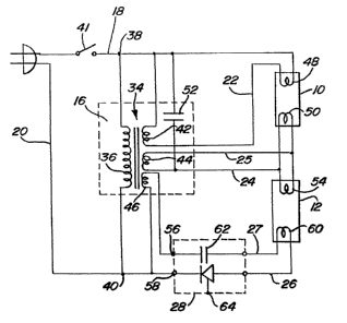
Referrinq now to the drawings in detail,, Figure 1
~ .
diagramically illustrates a pair of series connected electron
discharge devices 10 and 12, such as fluorescent lamps,
connected to an AC voltage source 14 through a standard ballast
circuit 16. The power lines 18 and 20 extend from the source
1~ to the high voltage side of the ballast circuit which has a
low voltage side from which outputs are applied across the
electron discharge lamps 10 and 12 under starting and running
conditions. In accordance with the present invention, a
current controller 28 is placed in one of the three low voltage
outputs of the standard ballast circuit for the series
connected fluorescent lamps 10 and 12 in order to modify the
characteristics of the output voltage and current otherwise
operative to fire and run the lamps.
Figure 4 illustrates a standard wave form curve 30
characterizing a typical output signal of the ballast circuit
having a sloping square wave shape. `Curve 32 represents the
output signal modified by the current controller 28, exhibiting
a decrease in voltage amplitude without any change in phase~ -
.
: - 6 -
i
.
~ . .
~ - ' ~ ` . .
r~ ' )
1 3248 1
The effect of such output signal modification is to apply a
potential difference across the filaments of lamp 12 less than
the firing voltage applied to lamp 10 during start-up in order
to ignite both lamps with a reduced current. Further, the
~overall operating temperature of the ballast 16 is typically
reduced from 60 to appro~imately 45 to effectively prolong
ballast circuit life. Also, firing of the lamps at a lower
temperature increases their life expectancy.
Figure 2 illustrates in greater detail a series
reactor type of standard ballast circuit 16 including a
transformer 34 having a primary winding 36 connected across the
AC voltaqe source through lines 18 and 20 at its opposite
terminals 38 and 40 upon closing of an on-off power switch 41.
Three secondary output windings 42, 44 and 46 are associated
with the transformer 34. Secondary winding 42 is connected at
one end to the terminal 38 of the primary winding and at its
other end to cathode filament 48 associated with lamp 10
through output line 22. The filament 48 is connectèd directly
to line 18 to which the primary winding terminal 38 is also
connected. The opposite cathode filament 50 of lamp 10 is
connected across the secondary winding 44 by output voltage
lines 24 and 25. A starting capacitor 52 is connected across
lines 18 and 24 to shunt the filaments 48 and 50 and complete
~, .
.
~.............. .....
~ .
- ' 1 32~81 1
the ballast circuit, as is well known in the art, for the
purpose of assisting starting, reducing shock hazard, and
minimizing transference of EMF to the ballast circuit.
he filament 50 of lamp 10 is interconnected in series
with one filament 54 of lamp 12 and both filaments 50 and 54
are interconnected in parallel to the secondary output winding
44 in lines 24 and 25. The secondary output winding 96 is
connected across the input terminals 56 and 58 of the current
controller 28 through which a low voltage output of the ballast
16 is applied by lines 26 and 27 to the other cathode filament
60 of lamp 12. Input terminal 58 is directly connected to
terminal 40 o~ the primary winding to which input voltage line
20 is connected.
The current controller 28 as shown in Figure 2
includes a regulating capacitor 62 connected to secondary
winding 46 through terminal 56 for cyclic or periodic
recharging. A current rectifying diode 64 is connected in
series with the filament 60 and the capacitor 62 between the
terminals 56 and 58 of the secondary winding 46. Such
capacitor~diode network when activated will change the expected
magnitude of the voltage potential of the system as reflected
by curve 32 shown in Figure 4 and by measurement of the volt
drop across capacitor 62, which is at least 100 VAC depending
on its size. A pulsating DC current is fed by diode 64 to the
-- 8 --
1 3248 1 1
filament 60 to maintain a nonfiring potential difference across
filaments 60 and 54. Additionally, capacitor 62 discharges
through filament 60 raising the potential on diode 64 and
filament 60 during each current blocking phase of the capacitor
.~.. . chargingccycle. A pulsating action is thereby achieved by the
- interaction of the diode 64 and the capacitor 62 because of the
- volt drop across filament 60 during the running operation under
a steady state voltage restricted to lamp 10 to achieve a
reduction in current drawn and decrease in temperature~
: In the embodiment illustrated, the AC source voltage
source has an operating voltage of 120 VAC to 347 VAC at a line
frequency of approximately 50 to 60 Hz, while the regulating
capacitor 62 has a capacitance value of approximately 2 to 7
microfarads, depending on the desired lumen output level of the
lamps~ The capacitor 62 ;s further more non-poled so that a
~ low AC output at terminals 56 and 58 of approximately 3 to 4
:~ VAC may charge the capacitor negative or positive dependent on
phase determined by diode 6~ When the capacitor charge
reaches a sufficient level applying firing potential to
. filament 60, both capacitor 62 and 52 discharge after firing
i lamp lQ~ Capacitor 62 then recharges as a result of the plasma
induced current flow between filaments in lamp 12. Such
push-pull action of the current controller 28 accounts for the
output voltage modification aforementioned and the decrease in
current and temperature conditions~
;~
.. ~, ' . ,
-
1 324~ ~ ~
In order to avoid malfunction under low level powerconditions experienced in some installations, a modified form .
of controller 28', as shown in Figure 3 may be utilized as a
replacement for the current controller 28 described with
respect to Fiqure 2. Current controller 28' includes a
regulating capacitor 62' and diode 64' which are interconnected
between the output terminals 56 and 58 of secondary winding 46
and the filament 60 to perform functions similar to those of
capacitor 62 and diode 64 as herebefore described. A full wave
voltage rectifier 68 is also connected across the winding
terminals 56 and ~8 to supply a rectified DC voltage.`for drive
of a timing circuit 70~ The output terminals of rectifier 68
are connected to the power terminals of an intergrated circuit
chip 72 of the timing circuit, across which a filter network is
formed by parallel connected resistor 74 and capacitor 76. The
input terminal of chip 72 is connected to the junction 78
between the resistor 80 and capacitor 82 connected in series
across the output terminals of rectifier 68. The output of
timing circuit 70 is connected to a switch actuator 84 of a
switching control circuit 86 having a bypass switch 88. The
bypass switch 88 is connected in series with resistor 90 across
the càpacitor 62'. A discharge resistor 92 is also connected
across the capacitor 62'. Upon closing of the power switch 41
to initiate start-up operation of the lamps, the timing circuit
.
- 10 -
.
r
` , , ' ` .'
.'~' '` , ~ `
,, ` ".` ` ' .
' ' ` ~ ` ' ,
1 3248 1 1
70 is triggered into operation to close switch 88 thereby
bypassing the capacitor 62' through resistor 90. Full
available power is thereEore applied to filament 60 for a timed
period to allow the lamps to be properly fired under a
conventional ignition cycle. At the end of such time delay,
the switch 88 is opened by the timing circuit so that the
current reducing action of the current controller 28' may be
in;tiated with cyclic charge of the aiding capacitor 62' under
the phase detecting and current blocking action of diode 64 as
hereinbefore described with respect to Figure 2.
The foregoing is considered illustrative only of the
principles of the inventions. Further, since numerous
modifications and changes will readily occur to those skilled
in the art, it is not desired to limit the invention to the
e~act construction and operation shown and described, and
accordingly, all suitable modifications and eguivalents may be
resorted to, falling within the scope of the invention.
What is claimed is as follows: `
.
!
11
.