Note: Descriptions are shown in the official language in which they were submitted.
~325292
,
1 --
'
Adhesive tape for bonding chips thereon
The present invention relates generally to a system
for mounting a chip, for example, a semiconductor chip,
on a package or the like, and, more particularly, to chip
mounting apparatus employing an adhesive tape for trans-
porting a large number of chips bonded thereon to adesired position.
During a manufacturing process, chips, for example,
semiconductor chips, chip capacitors, and chip resistors,
are generally transported successively from one location
to another while bonded to an adhesive tape. Accordingly,
, when such chips are to be mounted on a package or the
like, it is necessary to pick them up one by one from the
tape. A vacuum pickup method is generally employed for
this purpose, since the circuit, electrodes and the like
formed on the surface of each chip are required to be kept
out of contact with any hard member or substance.
To enable the prior art to be described with the aid
of a diagram, the figures of the drawings will first be
described.
Fig. 1 is a fragmentary side view, partly in section,
of the main portion of a conventional chip mounting
!,'j apparatus;
Figs. 2a to 2c are views showing several patterns
' during the positioning of the chip;
Fig. 3 is a perspective view of a chip mounting
apparatus according to an embodiment of the present
invention;
Fig. 4 is a fragmentary side view, partly in sectionr
~- of the main portion of the chip mounting apparatus of Fig.
. 3;
.. ~
.. - ~ , -
:`
-
- 2 - 132 ~292
Fig. 5 is a view similar to Fig. 1, according to an
embodiment of the present invention;
Fig. 6 (with Fig. 1) is a sectional view of an adhesive
tape, on which a plurality of chips are bonded, according
to one preferred embodiment of the present invention; and
Fig. 7 (with Fig. 5) is a view similar to Fig. 6, which
shows a modification of the adhesive tape.
As shown in Fig. 1, a plurality of chips 2 are bonded
onto an adhesive tape 1 to be supplied into a location
between a vacuum pickup collet 3 and a push rod 4. The
collet 3 has at its lower surface a suction port 5 which
has the same configuration and size as the chip 2, and
communicates with vacuum means (not shown), such as a
vacuum pump or the like. The push rod 4 has a coned top
and is secured inside a hollow cylindrical member 6, with
a space 7 between the rod 4 and the member 6.
In such apparatus, when one of the chips 2 on the tape
1 is positioned between the push rod 4 and the collet 3,
the push rod 4, together with the member 6, is moved
upwards to push the tape from below. The chip 2 is then
~ drawn into the suction port 5 of the collet 3 to be picked
;~ up thereby.
In such a vacuum pickup of a chip 2, however, it is
; necessary to match the center of the chip 2 with the tip
of the push rod 4. If the position of the former deviates
from that of the latter, the chip 2 is sometimes not
properly picked up. As a result, the chip 2 becomes
inclined to or drops off the collet 3 to be subject to
damage. Because of this, the conventional apparatus is
~30 provided with monitor means (not shown) for ensuring that
;~ the chip 2 is properly positioned with respect to the
member 6.
The positioning of the collet 3 and the push rod 4 is
; carried out prior to the positioning of the tape 1. In
this event, the monitor means recognizes the pattern shown
in Fig. 2a. The tape 1 with a plurality of chips 2 thereon
is then moved into position above the rod 4 so that one of
1~
:
:' : . '~ '` ~- -
: ~- :. , ,
" , - : - - . , .. . . . , . ,. :
1325292
-- 3 --
the chips 2 can be accurately positioned with respect to
the member 6 by pattern recognition. In this method, the
positioning between the tip of the push rod 4 and the chip
2 is achieved by way of the member 6. After this position-
ing, the chip 2 is pushed upwards by the rod 4 to be held
by the collet 3.
. However, the conventional chip mounting apparatus is
disadvantageous in that this accurate positioning cannot
be easily achieved. More specifically, if the chip 2 has
a small reflectance, a clear pattern of the chip 2 cannot
be recognized in contrast with that of the member 6,
resulting in insufficient pattern recognition. In other
words, there is insufficient contrast because the bright-
ness of the pattern of the space 7 is not sufficiently
different from that of the chip 2, as shown in Fig. 2b.
In the manufacture of a semiconductor device, such as
-i
an IC (Integrated Circuit), a large number of semiconductor
elements are initially formed into a pattern on a semi-
conductor wafer. These elements are then individually
separated from one another and each of the separated
` elements is mounted on a package or on a lead frame through
j die-bonding, by brazing or other means. During separation,
the semiconductor wafer is cut into individual semiconduc-
tor chips by dicing, dicing and braking, or scribing and
.i
breaking. In consideration of the workability in the next
die-bonding process, the semiconquctor wafer is cut into
small squares while the wafer is bonded onto an adhesive
tape. The semiconductor chips are then separated indi-
vidually from one another by extending the tape. On the
other hand, during the die-bonding process, the semiconduc-
tor chips individually separated on the tape are picked up
one by one to be transported onto the package or lead
frame.
; However, the conventional adhesive tape 1 has the
property of reflecting light. Because of this, when the
monitor detects light reflected from the tape 1, it becomes
difficult to distinguish the contour line of the chip 2
'~'
'~ ~
~,
... ... : ~ ..
'': , ;
-.~ :
. ,!
,
_ 4 _ ~32~292
- from the tape 1. As a result, since a clear pattern
recognition of the chip 2 cannot be achieved, the accurate
positioning of the chip 2 becomes difficult.
Accordingly, the present invention has been developed
with a view to substantially eliminating the above des-
cribed disadvantage inherent in the prior art, and has for
its essential object to provide an improved adhesive tape
that makes it possible to readily achieve clear pattern
recognition of each chip.
Another important object of the present invention is to
- provide an adhesive tape of the above described type that
is simple in construction and can be readily manufactured
at a low cost.
To this end, the invention consists of an adhesive
tape for use in a chip mounting apparatus in which light
is applied to one of a plurality of chips bonded on said
adhesive tape to detect the position of said chip, said
, adhesive tape comprising: a base layer; a film laminated
on at least one surface of said base layer and having a
reflectance with respect to light applied thereto different
from the reflectance of said chip; and an adhesive layer
laminated on either one of said base layer and said film
to bond said chip thereon.
The invention also consists of a chip mounting appar-
atus for mounting a plurality of chips bonded individuallyto an adhesive tape, comprising: a movable hollow cylin-
j drical member disposed below said chips; a push rod having
a coned top supported inside said cylindrical member to
push one of said chips from below; a vacuum pickup member
for picking up said chip pushed up by said push rod bysuction; a monitor means for detecting the position of
said chip with respect to said cylindrical member by
pattern recognition to match the center of said chip on
said adhesive tape with the tip of said push rod; and a 35 light source disposed inside said cylindrical member to
emit light from said cylindrical member towards said
. . .
.. ,~.
;. _
... .
. . .
.. ~ . . .-: .
-~
132~292
- 5 -
monitor means so that said monitor means can monitor a
contour of said chip with respect to said cylindrical
member.
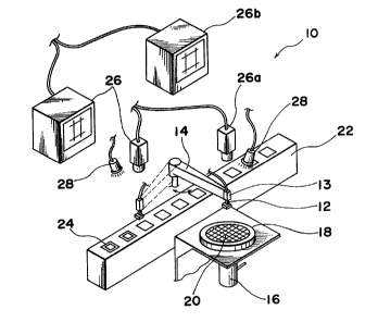
~- Referring first to Fig. 3, a chip mounting apparatus
according to an embodiment of the present invention,
generally shown by 10, comprises a vacuum pickup collet
12, a holder 13 for securely holding the collet 12, an arm
14 having one end rigidly secured to the collet holder 13
and the other end coupled with a driving means tnot shown),
a movable hollow cylindrical member 16 located below a
wafer ring 18 on which a large number of individually
separated semiconductor chips 20 are placed, a work tran-
; sport device 22 for transporting packages 24 or lead
frames placed thereon, monitor means 26 for monitoring the
position of each semiconductor chip 20 held by the collet
12 with respect to the member 16 and the package 24, and
a lighting system 28 for applying light to the semicon-
, ductor chip 20. The holder arm 14 is, for example, a
robot hand for driving the collet holder 13 in three
dimensions. the monitor means 26 is comprised of two sets
of a monitor camera 26a and a display 26b, respectively,
for detecting and displaying the position of the semicon-
ductor chip 20 with respect to the member 16 and the
package 24. The lighting system 28 includes two lamps
for applying light to the chip 20. One of the lamps 28
is located in the vicinity of one monitor camera 26a and
above the wafer ring 18, so as to apply the light to a
chip 20 placed on the wafer ring 18. The other lamp 28 is
located in the vicinity of the other monitor camera 26a
' 30 and above the work transport device 22, so as to apply the
light to the chip 20 that has been picked up by the collet
12 from the wafer ring 18 and is about to be attached to
one of the packages 24 placed on the work transport device
22. Accordingly, the collet 12 is free to move in three
~, 35 dimensions between a location where one of the chips 20
is picked up from the wafer ring 18 and another location
where this chip 20 is attached to the package 24.
.. " ~ .
i~
., .
. , ,
- :
. . ::
~. .
.
- 6 - 1~2~292
As shown in Figs. 4 and 5, a plurality of semiconductor
chips 20 placed on the wafer ring 18 are cuased to adhere
to an adhesive sheet or tape 30 for bonding the chips 20
thereon.
When one of the chips 20 is removed from the tape 30
and placed onto one of the packages 24, the collet 12 and
a push rod 32 are located above and below the chip 20,
respectively. The collet 12 communicates with vacuum
means (not shown) and has at its lower surface a suction
port 12a for holding the chip 20 by the vacuum. The push
- rod 32 has a coned top and is inserted from above into a
first recess 16a formed in an upper portion of the member
16. The push rod 32 is rigidly secured at its proper
.:;
position inside the member 16 by suitable engagement
between these two parts. The member 16 is free to move in
both the horizontal and vertical directions. Upon upward
movement of the member 16 together with the push rod 32,
the chip 20 is pushed up by the push rod 32 towards the
suction port 12a of the collet 12.
The member 16 is also provided with a second recess
16b communicating with the first recess 16a in which the
push rod 32 is rigidly secured. The second recess 16b
accommodates a light source 34 such as a lamp, an LED
.,i
(Light Emitting Diode) or the like. An optical plate 36
is securely supported above the light source 34 in the
second recess 16b by means (not shown). Accordingly,
when the light source 34 is supplied with electric power,
,
it emits light from the upper portion of the member 16,
through the second and first recesses 16b and 16a. In
this event, the optical plate 36 glows white by receiving
light from the light source 34. This light then enters
the monitor camera 26a to project the chip 20 on the
display 26b.
The positioning of the push rod 32 can be readily
achieved by moving the member 16 and by projecting a
pattern of the push rod 32 on the display 26b with the
push rod 32 properly positioned inside the member 16.
.....
.,,
'.'.`, ~
. . .
_ 7 _ ~32~2~2
- In subsequent positioning of the chip 20, the chip 20
is supplied between the collet 12 and the push rod 32 with
the chip 20 bonded to the adhesive tape 30. During this
positioning, the light source 34 emits light through the
first recess 16a of the member 16, so that the monitor
means 26 can detect the light. As a result, the pattern
of the first recess 16a becomes bright, as shown in Fig.
2c, whereas that of the chip 20 having a small reflectance
is still dark. The clear contrast between the patterns
of the first recess 16a and the chip 20 facilitates the
` accurate positioning of the chip 20. Accordingly, since
the tip of the push rod 32 and the center of the chip 20
coincide with each other, the chip 20 can be properly
gathered by the collet 12.
It is to be noted that the light source 34 can be
`i arranged outside the member 16 and the light emitted
therefrom can be introduced into the member 16 by way of
a light guide means such as an optical fiber or the like.
r' It is also to be noted that the optical plate 36 can
be omitted from the member 16.
It is further to be noted that, in this embodiment,
although the push rod 32 is rigidly secured inside the
member 16, the former can be arranged to be vertically
movable inside the latter. In this case, upon upward
movement of the push rod 32 within the member 16, the
collet 12 can properly receive and hold the chip 20.
Figs. 6 and 7 each depict the nature of an adhesive
tape according to an embodiment of the present invention.
Clear pattern recognition can also be achieved by the
~ 30 conventional chip mounting apparatus of Fig. 1 employing
; therein an adhesive tape according to the present
invention.
As shown in Fig. 6, the tape 30 consists of a base
layer 32 of extendable soft plastic, vinyl or the like
, 35 having a predetermined thickness, an anti-reflection film
34 laminated on the base layer 32 and an adhesive layer 36
laminated on the anti-reflection film 34. The tape 30
"~
s.
, ~ ,
,
~. .
- . .
- 8 - 132~292
initially wound around a supply roll (not shown) is cut
into squares each of a configuration having a size greater
than the diameter of the semiconductor wafer. The tape
30 is then transferred to the dicing process where the
semiconductor wafer is bonded onto the adhesive layer 36.
The tape 30 is then extended so that the semiconductor
wafer bonded thereon is separated into small squares each
having a semiconductor chip 20. An adhesive primer of a
plastic type is preferably used as the adhesive layer 36.
The anti-reflection film 34 is so constituted as not
to reflect light and is interposed between the base layer
32 and the adhesive layer 36. The anti-reflection film 34
can be formed, for example, by coating a film having a
thickness in accordance with the wavelength of light to
be applied. However, since the tape 30 is extended after
dicing, it is necessary to adjust the thickness of the
film to be coated in accordance with the extension ratio.
Furthermore, black or gray plastic can also be used for
the anti-reflection film 34. This colored plastic can be
readily obtained by putting black pigment or the like in
the plastic. The anti-reflection film 34 can be readily
laminated on the base layer 32 by coating or spraying the
plastic or by soaking the base layer 32 into the molten
; plastic. Other materials having light absorbing properties
can be used as the anti-reflection film 34.
' The tape 30 having therein the anti-reflection film 34
and obtained in the above described manner can be used as
it is in the ordinary manufacturing process of the semi-
conductor chips 20. In the vacuum pickup apparatus for
- 30 picking up individual semiconductor chips 20 one at a
time, light is applied to one of the semiconductor chips
20 bonded on the tape 30 for its proper po~itioning. The
light applied to the semiconductor chip 20 is reflected
from the surface thereof, whereas the light applied to the
.;:
tape 30 is prevented, by the anti-reflection film 34, from
-~ being reflected therefrom. Accordingly, since the monitor
means 26 detects only the light reflected from the chip
:
',~. ~,
.:,,- . : .
~32~2~2
20, it can clearly determine the contour of the chip 20,
and therefore positioning of the chip 20 by pattern
recognition can be accurately and readily achieved.
The anti-reflection film 34 of Fig. 6 can be replaced
by a light diffusion film 34a. The light diffusion film
34a interposed between the base layer 32 and the adhesive
- layer 36 is so constituted as to diffuse the light. To
this end, for example, a soft plastic having the property
of diffusing the applied light can be used for the film
34a. Such a film 34a can be readily obtained by putting
fine particles into the plastic. The film 34a can be
laminated on the base layer 32 by coating or spraying the
plastic or by soaking the base layer 32 into the molten
plastic.
When the tape 30a is formed in this way, the light
applied thereto is diffused in all directions by the film
34a. Accordingly, the monitor means 26 detects the light
reflected from the chip 20 to a far greater extent than
that from the tape 30, and can therefore clearly monitor
the contour of the chip 20.
Furthermore, the anti-reflection film 34 of Fig. 6 may
be replaced by a reflection film 34b. The reflection film
; 34b interposed between the base layer 32 and the adhesive
layer 36 will be so constituted as to reflect the majority
of the light. Such reflection film 34b can be formed, for
example, by coating on the base layer 32 a film having a
reflection ratio in accordance with the wavelength of the
light to be applied. A metal such as aluminum or the like
can be used for the film 34b. The film 34b can be readily
~- 30 formed on the base layer 32 by coating or spraying the
reflection material or through vacuum evaporation.
;~ Light applied to the chip 20 bonded on the tape 30b
partly reflects from the surface of the chip 20, whereas
light applied to the tape 30b is mostly reflected by the
reflection film 34b. Accordingly, the monitor means 26
detects the reflected light from the tape 30b to a far
greater extent than that from the chip 20. Thus clear
.,
.: : -
- , .
132~292
-- 10 --
recognition of the contour of the chip 20 can facilitate
the correct positioning thereof.
Fig. 7 depicts a modification of the adhesive tape of
the present invention.
As shown in Fig. 7, the tape 30c consists of the
extendable base layer 32, the adhesive layer 36 laminated
on one surface of the base layer 32 and a light scattering
film 34c for scattering light applied thereto laminated on
the other surface of the base layer 32. The light scatter-
ing film 34c can be formed, for example, by coating on the
base layer 32 a film containing fine particles of alumina
or the like and transparent fine particles. More specific-
ally, the film 34c can be readily laminated on the base
layer 32 by coating or spraying the aforementioned material
for scattering, or by soaking the base layer 32 into the
-` molten plastic containing this material.
Unlike the above described chip fastening tape 30, 30a
or 30b, an additional light source 40 is required located
below the tape 30c to direct light towards the lower sur-
face thereof. The light scattering film 34c scatters this
light. Accordingly, only light scattered from portions of
the tape 30c having no chip thereon can enter the monitor
~3 means 26, which clearly silhouettes the chip 20, thus
', facilitating the accurate positioning thereof by pattern
;~ 25 recognition.
Although the present invention has been fully described
by way of examples with reference to the accompanying
drawings, it is to be noted that various changes and
modifications will be apparent to those skilled in the art.
i 30 Therefore, unless such changes and modifications otnerwisedepart from the spirit and scope of the present invention,
they should be construed as being included therein.
. .
. .,
....
:
:~. - : - ,.... .