Note: Descriptions are shown in the official language in which they were submitted.
:
3 2 ~
.. ~ BACKGROUND OF THE INVENTION
Moderndevelopments intelecommunications technology
- have lead to integrated services communications
: `
transmission and switching systems for narrow band and
, ,~
;~ broadband communications services that have light
~ waveguides in the region of the subscriber lines as a
.~ i
:.: transmission medium. The light waveguides provide both
~; narrow band communication~ services such as, in
particular, 64 kbit/s digltal telephony as well as
~`, broadband communications services such as, in particular,
140 Mbit/s picture telephone. As a result narrow band
` signal switching matrix networks and broadband signals
~ switching matrix networks (preferably having shared
:~ control equipment) can also be provided side-by-side in
.~3 the switching centers (see German Patent 24 21 002).
:,...
i A known broadband signal switching matrix network
(see, ~or examplel European Patent Al 0 262 479) has a
~Z cross-point matrix in FET technology whose switching
~, elements are each formed with a switching transistor that
.l has its control electrode charged with a through-connect
3; or inhibit signal and has its main electrode connected
to the appertaining matrix output line. The switching
.~ elements each have a series transistor ~orming a series
."
circuit with the switching ransistor. This series
~, transistor has its control electrode connected to the
appertaining matrix input line and its main electrode
connected opposite from the series circuit being
:. j
connected via a sampling transistor to one terminal of
; an operatiny voltage source to whose other terminal the
~i1 respective matrix output line is connected via a prs-
~, 2
,., .:
` ~ 'I
~ ~2'3'~
:'`
charging transistor. The pr~-charging transistor and
sampling transistor are respectively charged oppositely
from one another at their control electrode with a
switching matrix network selection clock that subdivides
~`` a bit through-connect time span into a pre-charging phase
and into the actual through-connection phase. As a
~' result the matrix output line, for an inhibited sampling
transistor, is at least approximately charged in every
preliminary phase to the potential at the other terminal
o~ the operating voltage source.
, This known broadband signal switching matrix network
.. "~! that can have sampling transistors individually
associated to the switching elements or sampling
transistors, which are individually associated to the
i matrix input line or matrix output line, requires
separate clock lines that run through the cross-point
..',
matrix for selecting these sampling transistors. This
~ requires a circuit surface space requirement and involves
,~ a corresponding capacitative load on the matrix output
;~ lines. In order to guarantee adequate protection against
, i
signal interference, clock distribution and couplings
~, between matrix input lines and matrix output lines
~ require adequately high signal amplitudes on the matrix
s output lines, thi~ involving a relatively high power
`~ consumption.
:,
1 SUMMARY OF THE INVENTION
`3i An object of the present invention is to provide a
; broadband signal switching matrix network having limited
dissipated power given ade~uate protection against
.j
disruption in which such disadvantages are avoided.
.i
::3 3
~i~
. . .
.
The present invention is directed to a broadband
signal switching matrix network having a cross point
matrix in ~ET technology whose inputs can each be
connected to an input driver circuit, whose outputs are
provided with an output ~mplifier cir~uit, and whose
switching elements, which are controlled by a holding
memory cell, are each formed with a series circuit of a
switching transistor that has its control electrode
charged with a throughrconnect or inhibit signal and an
input transistor that has it~ control electrode connected
to the appertaining matrix input line. The series
circuit has the main electrode of one transistor, that
is connect~d opposite from the series circuit, connected
to the appertaining output line, the matrix output li~e
being connected to the one terminal of the operating
voltage source via a transistor. ~his broadband signal
switching matrix n~twork is inventively characterized in
that the main electrode of the other transistor, that is
connected opposite from the series circuit, is
continuously connected to the other terminal o~ the
operating voltage source. Also the transistor series
circuit of every switching element forms the cross-point-
. . .
i, associated, one branch of a differential amplifier whose
... ~
other branch, shared by the cross-points connecting to
one and same output line, is formed by an output
amplifier circuit individually associated to the matrix
~i output line. The output amplifier circuit has a series
circuit of a first transistor that has its control
~;,j electrode connected to the other terminal of the
~ "
~ operating voltage source and of a second transistor
. .~
:'i
~J 4
: .,
.
, :"
~. ,!
'; :~ ' '
" '.~
; :' '~ ' ~ . , ' ' . '
2 ~
having its control electrode connected to a reference
voltage. The seri~s circuit has the main electrode of
the one transistor, that is connected opposite from the
series circuit, connected to the ~ppertaining matrix
output line and that main electrode of the other
transistor, that is connected opposite from the series
circuit and connected to the amplifier output, connected
via a load transistor to the other terminal of the
operating voltage source.
In addition to providing the advantage that the
switching matrix network does not require a clock signal
and, thus, corresponding clock lines either for potential
~, 1
:1input driver circuits or Por the cross-point matrix
.~ ,~ i,
~,itself or for the output amplifier circuits and that the
entire bit through-connect time span, unshortened by a
,., I
pre-charging phase, is thus also available for the
through-connection of the respective bits, the present
inv~ntion provides a further advantage that the input
, .
~.~'line can be operated with an extremely small signal boost
:; ~
~jof, for example, one volt for an operating voltage of,
.for example, five volts. This produces a corresponding
1reduction of the signal couplings from the matrix input
,..~1
.1lines onto the matrix output lines and, thus, a reduction
~.~
.~in the dissipated powers. At the same time, the possible
-reduction in signal boost on the matrix input line, just
like the omission of a pre-c~arging phase, also produces
., :i
~:-ia reduction in disturbances of the operating voltage of
-~ `1
. Jthe broadband signal switching matrix network caused by
~1,power peaks. Moreover, the ~'distributed'~ di~ferential
:~.amplifier provided according to the present invention
:. ~
.~j 5
20365-2953
also exhibits the known advantages o~ tradi.tional diE~erential
amplifiers.
In a further development of the present invention,
the transistor series circuit of every switching element can
have its input transistor connected to the matrix ou-tput line
and the transistor series circuit of the respective output
amplifier can have the second transistor connected to the
. 1
matrix output line. Alternatively thereto, however, it is
;.. ~ possible that, in a Eurther development of the present
invention, the transistor series circuit of every switching
element has its switching transistor connected to the matrix
output line and the transistor series circuit of the respective
output amplifier can have its first transistor connected to the
~ .
matrix output line. This avoids a capacitative loading of the
ma-trix output line by the channel capacitance of the series
transistors of switching elements that are not through-
connected.
, In a further development of the present invention,
~i( the transis-tor series circuit of every switching element can be
connected to the other terminal of the operating voltage source
via a load transistor. This produces a corresponding symmetry
of both branches of the respectively fashioned differential
` amplifier.
Therefore, to summarize, according to a first broad
¦ aspect, the invention provides a broadband signal switching.,lj
;~ matrix network connec~ed to an operating voltage source and~`1
having a cross-point matrix with cross points in FET
technology, inputs which are respectively provided with an
I
-. input driver circuitl the input driver circuit connecting the
1~ 30 input to a matrix input line, and outputs which are each
.~. provided with an output amplifier circuit, the output ampli:Eier
circuit connecting the ou-tput to a matrix output line and
t,~
.~, ~ .
~"; . . ~
`` ~ 32~ 20365-~953
:~ having switchlng elements, respectively controlled by a holding
~ memory cell, each switching element being formed with a series
circuit oE a switching transistor that has a control electrode
charged with a through-connect or an inhibit signal and of an
input transistor that has a control electrode connected to the
appertaining matrix input line, the series circuit having a
:: main electrode of one transistor of the switching and input:`~ transistors that is connected opposite from the series circuit,
; connected to the appertaining matrix output line whereby the
~ 10 matrix output line is connected to a terminal of the operating
, (
voltage source via a transistor, and having a main electrode of
the other transistor of the switching and input transistors
that is connected opposite from the series circuit, permanently
connected to another terminal of the operating voltage source;
` and the series circuit of the switching and input transistors
.~ of every switching element forming a cross-point, one branch of
: a differential amplifier, which has another branch shared by
the cross-points connected to one and same output line, formed
~.~
:~ by the output amplifier circuit individually associated to the 20 matrix output line, the output amplifier circuit having a
series circuit of a first transistor that has a control
: electrode connected to one of the terminals of the operating
~! voltage source and of a second transistor that has its control
.,
:- electrode charged with a reference voltage, the series circuit
,i '
of the first and second transistors having a main electrode of
one transistor o-E the first and second transistors that is
connected opposite from the series circuit, connected to the
appertaining matrix output line and a main electrode of the
,
. other transistor oE the :Eirst and second transistors that is
j~ 30 connected opposite from the series circuit and that is
connected to the amplifier output connected to one oE the
;l
' 6a
.,.. ~; ,
~ 3 2 ~ ~ 6 9 20365-2953
.; terminals oE the operating voltaye source via a load
~ transistor.
~ccording to a second broad aspect o:E the invention,
: there is provided a broadband signal switching matriY~ network
,,
connected to an operating voltage source and having a cross-
point matrix with cross-points in FET technology, inputs which
~` are respectively provided with an input driver circuit, the
input driver circuit connecting the input to a ma-trix input
line, and outputs which are each provided with an output
amplifier circuit, the output ampliEier circuit connecting the
output to a matrix output line; and having switching elements,
respectively controlled by a holding memory cell, each
1 switching element being formed with a series circuit of a
:. switching transistor that has a control electrode charged with
a through-connect or an inhibit signal and of an input
~1 transistor that has a control electrode connected to the
31 appertaining matrix input line, the series circuit having a
main electrode of one transistor of the switching and input
~ transistors that is connected opposite from the series circuit,
.~ 20 connected to the appertaining matrix output line whereby the
~I matrix output line is connected to a terminal oE the operating
. .
~i~ voltage source via a transistor, and having a main electrode of
the other transistor of the switching and input transistors
that is connected opposite from the series circuit, permanently
~ connected to another terminal of the operating voltage source;
: ! and the series circuit of the switching and input transistors
I of every switching element forming a cross-point, one branch of
.~ a differential amplifier, which has another branch shared by
''
the cross-points connected to one and same output line, formed
by the output amplifier circuit individually associated to the
.~ matrix output line, the output amplifier circuit having a
i., series circuit of a first transistor that has its control
:,
;`` 6b
-.
32~9
; 20365-2953
`~ electrode connected to one o:E the terminals of the operating
~ voltage source and of a second transistor that has its control
:s electrode charged with a reEerence voltage, the series circuit
'~'.;,,
~ of the Eirst and second transistors having a main electrode of
~ one transistor of the first and second transistors that is
' connected opposite from the series circuit, connected to the
; appertaining matrix output line and a main electrode of the
: other transistor of the first and second transistors that is
connected opposite from the series circuit and that is
.. 10 connected to the amplifier output connected to one of the
terminals of the operating voltage source via a load
transistor, a feedback CMOS inverter being provided as the
reference voltage source, each input driver circuit preceding
the matrix input lines being formed wi-th a feedback MOS
inverter having the same transistor dimensions that forms a
ring circuit with a further, feedback CMOS inverter circuit
.~.
, whereby this further CMOS inverter circuit has a series circuit
. of two transistors in each of its two circuit branches, the
.,
.~ respectively inner transistor thereof having its control
electrode connected to the input of the broadband signal
switching matrix network.
;.
` BRIEF DESCRIPTION OF THE DRAWINGS
The features of the present invention which are
believed to be novel, are set forth with particularity in the
appended claims. The invention, together with further objects
~:1 and advantages, may best be understood by reference to the ~ :
~7 following description taken in conjunction with the
i accompanying drawings, in the several Figures in which like
'` reference numerals identify like elements, and in which:
;, 30 Figure 1 is a schematic of a broadband switching
;:~ matrix network; :
'i'l
6c
:':
'.', .~
~ 3 2 i~ 20365-2953
, :~
,~: ' Figures 2-8 are circuit schematics o:E circuit-
. ~
~ oriented details oE the present invention.
,,,
, ,. " .
,: ..
.:;.
'`~'';'.
, ~; .
' '1,~'..,.
~ . . .
.,: ".~. .
.;
j
', ~ 1
"~ .l
:',,,~
.., ..~
~",, ,j
','..'' ,~,ij
''' ~1
:, 1
,'li,~,:`,.',!
'~
.,. . i, .
3l
i ;.', 1
. .'~'.''
. . 3
:'.:.. ~
...... . .
~'`:' ' ':i
: ~:`., :3
`'i
6d
~,
i f `-i
~2~3~
DESCRIPTION OF THE PR~FERRED EMBODIMENT
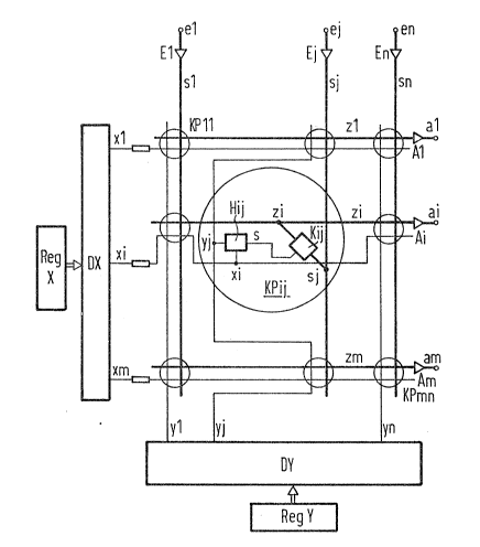
Figure 1 schematically depicts a broadband ~ignal
-~ switching matrix network in a scope required for an
understanding of the present invention. Input driver
circuits El...Ej...En are provided at the input
`~ el..... ej... en thereof that connect to column lines
, ' sl..... sj... sn o~ a cross-point matrix and the outputs
al...ai...am thereof reached by row lines zl...zi...zm
-1 of the cross-point matrix are provided with output
amplifier circuits Al...Ai...Am.
The cross-point matrix has cross-points
KPll...KPij...KPmn whose switching element (as is
!
indicated in greater detail in the case of the cross-
~i point RPij for the switching ~lement Kij thereof) can be
respectively driven by a cross-point associated holding
~i memory cell Hij (at the cross-point KPij) whose output
,1 s connecta to the control input of the respective
', switching element (Kij at the cross-point KPij).
' .:,1
According to Figure 1, the holding memory
I cells.. Hij... are driven in two coordinates by two
'~
selection decoders, namely, a row decoder DX and a column
decoder DY via corresponding selection lines
xl...xi...xm; yl..~yj...yn.
A~ may be seen from Figure 1, the two selection
,`~, decoders DX, DY may thereby be chargeable, proceeding
from input registers Reg X, Reg Y, with a respective
~, cross-point row address or, respectively, cros~ point
:i column address shared by a matrix line (row or column)
of cross points. In response theret~ they respectively
~" ~ ~
;~,, output a "1" selection signal to the selection line
.,l:;j
~, 7
"
.,.:,i .
~ t~i ." .~
' . i
'; ~!
~ 3 2 .:j $ 3
:
corresponding to the respective cross-point line address.
.` The coincidence of a row selection signal "1" and of a
~-- column selection signal "1" at the intersection o~ the
`~ appertaining matrix row with the appertaining matrix
column during the set-up of a corresponding call then
effects an activa~ion of the holding memory cell situated
~' there, for example, the memory cell Hij. This has the
. result that the switching element controlled by the
``:
appertaining holding memory cell (Hij) becomes
conductive, the switching element Kij in the example.
So that the switching element Kij und~r
. consideration in the example i~ again inhibited for a
clear down o~ the appertaining call, the selection
.. decoder DX is again charged with the appertaining row
address proceeding from the input register Reg X, so that . 3
the row decoder DX again outputs a row selection signal
, i
: . "1" on its output line xi. Simultaneously, the column
decod~r DY, proceeding from its input register Reg Y, is
~jl charged, for example, with a dummy address or with the
`~ address of a column of unconnected cruss-points, so th~t
~' $`J, it outputs a column selection signal "O" on its output
,. . :f '~
-"~ linc yj. The coincidence of row selection signal ~11" and
,!~,''~ column selection signal "O" then ef~ects the resetting , .
of the holding memory cell Hij, with the result that the
,::.~, switching element Kij controlled by it is inhibited.
.~ Tha holding memory cells... Hij... can be fashionad
in a known manner. Thus, the holding me~ory cells (as
known, ~or example, by European patent A 0 238 834 and
also sketched in Figures 5 and 6) can be formed with an
n-channel transistor Tnh and two cross-coupled inverter
.`'-'-`1
:~ j 8
:.,.::.`. . ~ :!
'.. ` 1 -
, ,!, , ' . .
", '. :
~2 D~
:~,
circuits (CMOS invert~r circuits Tp' Tn'; Tp'', Tn'' in
Figure 5; n-MOS inverter circuits Tnl', Tnl'; Tnl'', Tn "
in Figure 6), whereby one inverter circuit has its input
~ide connected to the appertaining decoder output yj of
the one selection decoder via the n-channel transistor
Tnh that in turn has its control electrode charged with
the uutput signal of the appertaining decoder output xi
of the other selectio~ decoder. One inverter circuit has
its output side connected to the control input s of the
appertaining switching element.
. ;.~
How the switching elements...Kij...can be realized
:
in circuit-oriented terms i~ illustrated in Figures 2,
' 3 and 4: the switching elements... Kij... are each formed
;', with a series circuit of a switching transistor Tk that
has its control electrode charged with a through-connect
,;
~, or inhibit signal proceeding from the holding memory cell
and o~ an input transistor Te that has its control
i ,.
-, electrode connected to the appertaining matrix input line
~; sjo The series circuit has the main electrode of the one
tran~istor Tk (in Figure 3) or Te (in Figure 2 and Figure
~' i 4), that is connected opposite from the series circuit,
~,, connected to the appertaining matrix output line zi. The
`1l matrix output line zi is connected to one terminal (UDD
'1 in Figure 3; Uss in Figure 2 and Figure 4) of the
, . ,. ~,
~ operating voltage source UDD U5S via a transistor Ti that
.,. ,..~
has its control electrode connect~d to a corresponding
bias voltage (USAI~ in Figure 3; UBIAS in Figure 2 and in
Figure 4). Th~ transistor Ti forms a current source
"~ together with the respective operating voltage source.
~ .: :.,,
The main electrode of the other transistor Te (in Figure
~. .:, ~
:;. i
, ~
~ 3 2 ,~
3 or, Tk (in Figure 2 and in Figure 4) that is connected
opposite from the series circuit is permanently connected
to the other terminals Uss, ~ground in Figure 3) or UDD
~in Figures 2, 4) of the operating voltage source. The
transistor series circuit Tk-Te o~ every switching
element Kij thereby forms the cross-point-associated, one
branch of a dif~erential amplifier whose other branch is
formed by the output amplifier circuit Ai individually
associated to th~ matrix output line and thus shared by
the cross-points connecting to one and the same output
i
., line zi. To that end, the output amplifier circuit Ai
,'. has a series circuit of a first transistor Tak that has
its control electrode connected to the other terminal,
" f
::: (Uss, ground in Figure 3; UD~ in Figures 2 and 4) of the
operating voltage source and o~ a sPcond transistor Tae
that ha~ its control electrode connected to a reference
`1 voltage (UFE~ in Figure 3; UREF in Figures 2 and 4). The
... ..
.~ series circuit has the main electrode of one transiætor
~1; Tak ~in Figure 3) or Tae (in Figures 2 and 4), that is
,: connected opposite from the series circuit, connected to
the appertaining matrix output line zi and has the main
electrode of the other transistor Tae (in Figure 3) or
Tak (in Figures 2 and 4), that is connected opposite from
.. the series circuit and connects to the amplifier output
.~. .i I
Ai connected to the other terminal (Uss~ ground in Figure
.;. ~ 3; UDD in Figures 2 and 4) via a load transistnr Tal that
`. may be connected to as a diode.
~, As Figures 2 and 4 show (differing from Figure 3),
.` the transistor series circuit Tk-Te of every switching
~ element Kij can be connected to the other terminal (Uss,
.,. .~,
., ,1 10
~ ., ,j .
,~ , .,. ; .,,
:" .~
- .. ~ .
; . ~,.~ . , - -
. .: ~
:1 ~ 2 ?3 ~ ~ 9
~ ground in Fiyure 3; UDD in Figure 2 and in Figure 4) o~
;:.
the operating voltage source via a load transistor Tl
connected as a diode. Such a load transistor yuarantee~
~ a correspondingly high symmetry of the differential
... amplifier respectively fo~med by switching element Kij
and output amplifier Ai and, necPssitates an additional
circuit area requirement. Thi~ area requirement iB
~ .~ eliminated by an elimination o~ the cross-point-
.~ . associated load transistor Tl (in Figures 2 and 4) that
~ involves a slight asymmetry of the differential amplifier
.;:
~ and therefore requires a slightly higher signal boost.
. :.,;
,` As may be seen from Figures 2 and 4, the transistor
~ series circuit Tk-Te o~ every switching element Kij can
., ' have its input transistor TP connect~d to the matrix
:. output line zi. In a corresponding fashion, the
',':", `:~1
-, transistor series circuit Tak-Tae of th output amplifier
.~ Ai, individually associated with the matrix output line,
'~i then has the second transistor Taa connected to the
~ matrix output line zi. Then~as seen proceeding from the
r,",~",:~ matrix output line zi, the input transistor Te is, in a
.:~ ,.,
sense, transparent, so that changes in signal status on
the matrix input line i~j can be transmitted onto the
~: '' `'.'1
matrix output line zi via the channel capacitance of the
input transistor Te even when the switching eliement Kij
inhibited.
~` This transmission can be avoided when the sequence
~., of input transistor Te and switching transistor Tk is
, '. 'l
interchanged in the tranisistor series circuit Tk-Te o~
every switching element Kij. As may also be iseen from
Figure 3, the transistor series circuit Tk-Te of every
; ! ~ ~ .`
....
~ 3 2 ~ ~ ~ 9
-`
~ switching element Xij then has ite switching transistor
., Tk connected to the matrix output line zi and, in a
:;~ corresponding way, the transistor series circuit Tak-Tae
~`- of the appertaining output amplifier Ai individually
. associated with the matrix output line has the first
.
.~` transistor Tak connected to the matrix output line zi.
According to the exemplary embodiment sketched in
Figure 4, a signal line dsel, connecting to the control
electrode of the output amplifier load transistor, Tal,
, is provided in addition to every matrix output line, zi,
:............... the load transis~or Tl of every switching element, Kij,
.,~.
:-: connected to the appertaining matrix output line, zi,
~ -.
. ~ being connected to the signal line dsel via an auxiliary
; ~
~ transistor Tkk that, just like the switching transistor
-.~ Tk of the appertaining switching element, Kij, is
`;, connected to the control input s thereof. A~ a result,
,i'~i! a differenti~l~to-single-ended conversion o~ the digital
signals through-connected via the appertaining switching
element is achieved with a current mirroring from the
. ...
. switching element branch onto the output amplifier branch
, ~ 1
.~. of the differential amplifier, formed by a switching
., element, Kij, and the output amplifier circuit Ai
" "I
l individually associated to the matrix output line, thus
.l, producing a signal amplification of 6dB but also
..
:,..
i~i involving a corresponding circuit space requirement and
,,... ,..~,
~`", power requirement.
~ s Figures 2-4 show, the transistors Te, Tae, Ti are
of the type complementary to the respective load
transistor Tal and, Tl in the respective, so to speak
:~J "distributed", differential amplifier formed by the
....
.~. 12
:.1 j
;'`'.'1
, '` ,,,. ' ~
, . .
~3 ~ 3 ?J~3$
;.~'.'
`~: switching element Kij and by the output amplifier circuit
~ Al.
,,~ ,
~.i Thus, according to Figures 2 and 4, the load
., .;
transistors Tal and Tl are of the p-channel type, whereas
output amplifier transistors Tae and Tak, current source
transistor Ti and input transistor Te of the respective
.:J
: ,~, switching element, Kij, and the respective switching
....l
`. transistor Tk as well in the exemplary embodiment, are
-~ of the n-channel type. The operating voltage source UDD-
, ' '
;-~ Uss thereby may output an operating voltage of, ~or
~,
example, five volts that is standard ~or C~OS circuits
from which a reference voltage UREF f, for example, two
volts or~ respectively, a bias U21AS of, for example, 1.5
volts that slightly exceeds the threshold voltage of the
current source transistor Ti of, for example, 1.2 volt
is capable o~ being derived by a voltage divider circuit
having corresponding dimensîoned transistors To, Tu and
having the form of a fedback inverter circuit, as
,
~-' depicted in Figure 7.
According to Figure 3, the output amplifier load
transistor Tal is o~ the n-channel type, whereas the
`` output amplifier transistors Tae and Tak, current source
. transistor Ti and input transistor Te of the respective
:.~ switching element, Kij, and also the respective switching
~;¦ tran~istor Tk in the exemplary embodiment, are Q~ the p-
channel type. The operating voltage source UDD_USS may
'.~, ~1
again output an opPrating voltage of, for example, five
. ~
volts that is standard for CMOS systems from which a
¦ reference voltage UFER of, for example, 3 volts or,
:I respectively, a current source transistor bias USAI~ ~
~:~1 13
. .~,i
i ~
`` ~32~79
, `...
...,~ `
`~ for example, 3.5 volts is capable of being derived, again
.. - by a voltage divider circuit as depicted in Figure 7.
In order to keep the individual ~witching elements,
Kij, optimally small, the gain of the "distributed"
.,
differential ampli~ier is kept relatively slight. For
a ~urther ampliEica~ion of the output signal that may be
-~ re~uired, the output ampli~ier circuit Ai individually
associated to the matrix output line can, ~or example,
be followed by a pseudo-p-MOS or n-MOS amplifier stage.
This, however, i5 no longer shown in the present
invention since it is not required for an understanding
of the present invention.
As we already set forth above, the reference voltage
i~' source for the output amplifier transistor Tae can be
formed by a fedback inverter operated as a voltage
divider connected to the operating voltage source UDD_
i Uss. Such a CMOS inverter/voltag divider circuit
.~l realized with a p-channel transistor To and with an n-i 3
channel transistor Tu is shown in Figur~ 7. The
l referenc~ voltage appearing at the output UFER of this
CMOS inverter operated as a voltage divider is thereby
,'~ ~! ` . `.
determined by the dimension of the two transistors To and
Tu.
The same transistor dimsnsions can also be shared
by the respective two transistors of fedback CMOS
inverters Tp-Tn (see Figure 8) that form in a respective
ring circuit together with a further fedback CMOS
inverter circuit Tq-Tr-Ts-Tt (see Figure ~) input driver
, !~
~ circuitsO.. Ej... provided at the inputs..... ei... of the
i broadband signal switching matrix network. Ring circuits
~. .,
,"~
~, 14
. ~ . ~, .
. ~
,. j ,
~` ;`~.
: :`
~ ~C32~
` `
.o~ two fedback C~OS inverters are known in the prior art
(see European Patent A 0 250 933). In the exemplary
.~,
embodiment depicted in Figure 8, the further CMOS
inverter circuit has a seri~s circuit of two transistors
Tq-Tr or TS-Tt in each of its two circuit branches, the
inner transistor Tr or Ts thereof having its control
electrode connectsd to the input ej of the broadband
signal switch matrix network.
The switching threshold of the CMOS inverter Tp-Tn
is established by the geometrical dimensions of its p-
channel transistor Tp connected to one terminal of the
operating voltage source UDD and of its n-channel
transistor Tn connected to the other terminal of the
operating voltage source Uss. When the dimensions of the
two ~orresponding transistors (To and Tu) are equivalent
in a re~erence voltage source fashioned as a CMOS
inverter/voltage divider circuit according to Figure 7,
the switching threshold lies at the reference voltage
output by this reference voltage ~ource. This results,
even for ~luctuations of the operating voltage UDD_USS or
. .,
for a modification of technological parameters, in that
the HIGH level and the LOW level of a digital signal,
through-connected via the broadband signal switching
matrix network proceeding from the switching matrix
network input ej, remain constant within broad limits
relative to the level of the reference voltage UREF (in
Figures 2 and 4) or UFER (in Figures 3 and 7) ef~ective in
: 1
the output amplifier circuit Ai (in Figures 2-4).
The respective height of the level is thereby
., determined by the geometrical dimensions of the p-channel
1 !
. ~, . ~ . . .
.,, ~ ~ : . ,
~ 3 2 ~ 5~
transistor Tq connected to the operating voltage source
UDD and of the n-channel transistor Tt of the further
-~ CMOS inverter circuit that is connected to the operating
: voltage source Uss. For a LOW signal appearing at the
, ~
switching matrix network input ej, the p-channel
transistor Tq of the further CMOS inverter circuit Tq-
:~ Tr ~s-Tt is connected parallel to the p-channel
.. transistor Tp of the fedback CMOS inverter Tp Tn via the
p-channel transistor Tr that is consequently
.,, transmissive, and, for a HIGH signal appearing at the
; switching Matrix network input ej, the n-channel
.:,
transistor Tt of the further, CMOS inverter circuit Tq-
. Tr-Ts Tt is connected parallel to the n~channel
transistor Tn of the fedback CMOS inverter Tp-Tn via the
-~ n-channel transistor Ts that, consequently, is
.l transmissive. This parallel connection modifies the
"`~ voltage division ratio respectively effective at the
.f, circuit point Q, so that, for the full CMOS signal Boost
I of, for example, five volts of the digital signals
`l appearing at the switchinq matrix network input ej (in
Figures 1 and 8), the signal boost of the digital signals
, appearing at the output of the input drive circuit Ej (in ` 1
:i:l Figures 1 and 8) and, thus, on the appertaining matrix
input line sj (in Figures 1 and 8) is reduced to a value
`" fl of ~ for example one volt. As may also be seen from
: Fiqure 8, these digital signals can thereby be buffered
; . `1
with a differential amplifier OP connected as a voltage
follower.
The invention is not limited to the particular
details of the apparatus depicted and other modifications
' ~ `i
~i 16
~ .
":
:
1 3 2 -J ~ ~ ~
..
.;
and applications are contemplated. Certain other changes
~ may be made in the above described apparatus without
.` departing from the true spirit and scope of the invention
' herein involved. It is intended, therefore, that the
-i subject matter in the above depiction shall be
;l interpreted as illustrative and not in a limiting sense.
,: .,~ ,
, " 1
, 1 . ~
;,
~,
:,
.,1
;``1
. i .
s ;.,~
.~
,;'l
.,,~.it
...~
,~ ~
:.
;,~
, 17
. ~, . ~ ~ . . .