Note: Descriptions are shown in the official language in which they were submitted.
32~7~
COM131NATION INDEX/GAIN GlJlDEDSEI\11~'0NDUCTOR
LASERS
BACKG120UND C)F Tl-IE lNVEN'rION
This invention relates to semiconductor ]asers and, in particular, to lasers
having a combination index guiding and gain guiding features.
.
~n conventional semiconductor lasers, the beam emitted from a facet of the
. j laser is usually focused to a small spot in order to meet the needs of various
; ~ applications, such as optical or magneto-optic disk storage and retrieval and
]aser printing, by means Or reimaging the laser near field pattern to the
desired imagc plane. Semiconductor lasers possess different points of origin
of divergence (also referred to as beam waste positions) as we31 as ang]es of
~, divergence for radiation emitted from the laser facet in directionsorthogonal to each other, i.e., in a vertical emission direction which is
-¦ perpendicu]ar to the p-n planar junction and in a latera] emission direction
: 1 which is parallel to and along the p-n p]anar junction.
. l .
These points of oligin of divergence also vary relative to different kinds of
. i ]aser geometry. One kind of laser geometry is the~refractive index guiding
i, lase~which depends on differences in the index of refrac~ion of materials
duè to either a diffusion, e.g., ZD, along the plane of the p-n junction to
create lateral waveguidance or to the structura] geometry of the laser, e.g.,
~, nonplanar layers, substrate channe]s or mesas, or ]ayer thickness variations
etc. to guide the propagating radiation by a rea] refractive index waveguide.
In these ]asers, the refractive index guiding referred to is a]ong the p-n
junction p]ane, although it need not be precisely at the plane. (It is
understood that perpendicular to the p]ane of the p-n junction the
i, heterostructure layers a]so create a refractive index waveguide~. Examp]es of
` 1 these lasers are the channeled substrate p]anar ]aser, the channeled substrate
~;,
: !
``!
:
' ' - -- . -
.. . , ~
~ 3 2 ,~
- 2 -
nonplanar laser and the buried heterostructure laser. ln an index guided
laser, the near ficld pattern of the 1aser can be imaged into a diffraction
` limited spot at an image plane with no correction for astigmatism because
the beam wastes in both the vertical and lateral direclions lie subs~ntially
in the plane of the laser facet. These lasers usually emit a narrow
wavelength spectrum and often single longitudina] mode operation is
~- obtained.
. .; .
The other kind of laser geometry is the gain guide laser. A ~ain guided lase
lo depends upon current dependent differences in both the real and imaginary
', part of the index of refraction of the semiconductor material comprising the
structural layers of the laser to guide the propagating radiation. The narrow
current confinement region, or narrow stripe, as the case may be, serves
several purposes. Although the threshold current density is somewhat
increased in operation of these lasers versus index guided lasers, the total
laser threshold current is greatly reduced relative to a wide stripe which
adds to minimize internal heating and thereby permitting continuous
operation. The current confinement geometry confines the optical wave
,
' j laterally in the p-n junction where no change in the rea~ part of the
., 20 refiractiYe index exists in the absence of injected charges. Thus, the high
` ' injected charge density and resulting high gain directly beneath the current
;, confining region deterrnines both the real and imaginary parts of the lateral
refractive index profile. This lateral waveguiding is totally dependent on the
~ injected charge distribution. As a result, the laser characteristics will depend
``'~'! 25 upon the widths of the current confining region.
:1
"'!1
As current confinement region widths decrease, power output increases
stably (with increasing current) in gain guided lasers and the lateral mode
does not shift. This improvement, however, occurs at the expense of an
increase in beam divergence along the p-n junction plane and greater beam
astigmatism, which is present in all gain guided lasers. Astigmatism occurs
because the wavefront curvature of the laser beam is greater for narrower
.
.~
, .. .
, ,
.
.
.
: : .
,, , "
~, .
.,.,. ~ ~
.. ,, ~ :
3~ ~ ~2~7~
current confinement widths. Since no such curvature occurs perpendicular
to the p-n junction plane, the beam waste in the p-n junction plane and in
the plane in the laser optical cavity perpendicular to the p-n junction plane
are at different spatial positions. Radiation in the vertical emission directions of the laser has a point of origin Or divergence or beam waste position well' within the laser behind the facet. Because of this factor, the image plane of
~ the beam in the ]ateral emission direction will not be in the s~me plane as
;~ the vertical emission direction to bring abou~ astigmatism upon focusing to
~` a common image plane requiring more sophisticated optical systems for
-' l0 collimation and refocusing.
~i In applications such as optical disk systems, printer systems or other such
applications requiring focusing of the near field output of a semiconductor
laser, it is decidedly advantageous to employ an index guided laser since
;;~ 15 these lasers do not exhibit the astigmatism of gain guided lasers thereby
, .
permitting easily accomplished fiocusing. However, index guided lasers
~, norrnally exhibit single longitudinal mode operation when operated at
'~`J power levels in excess of several milliwatts. In the previously mentioned
~, laser applications, single longituclinal mode operation leads to excess noise
.3 20 resulting from the long coherence ]ength of the laser radiation or
Iongitudinal mode "hopping" caused by therrnal variation of the laser
versus time. On the other hand, gain guided lasers will provide multi-
longitudinal mode operation relieving these undesirable effects but
-~ requiring a sophisticated lens system to remove the undesirable astigrnatism.
f SUMMARY OF THE INVENTION
.~i
~, According to this invention, a semiconductor laser is provided with the
combination of index/gain guiding attributes to alleviate the foregoing
3 30 disadvantages. The semiconductor laser is provided with one or more layers
~1 folming an active region for supporting radiation propagating under lasing
conditions in an optical cavity established between transverse end facets of
,.
,
.~
,:f
.` Z
" ~ .
?
'.`',''; ' ' , ,
:','` ,
'
.''; ' ' ' , . .
. ,, ` .
'','.''~ - ' :
.~'~, .
: ~.32~7~
;,
the laser and -the active region is characterized by having
' a combination index and gain guiding region. For optical
. .
disk and other applications previously alluded to, it may
be preferred that this combination region, be comprised
; 5 of a central gain guiding region and an index guiding
region between -the central gain guiding region and the
. laser end facets. Furthermore, the regions between the
central reyion and end facets may be provided with suf-
~ .,
ficiently thin active region thickness to form a synthe-
, 10 tic transparent or quantum well waveguide so as not to
be radiation absorbing due to the quantization of
electron states.
,.. .
', Alternatively, applications may arise wherein an astig-
~;i matic output beam emanating from a nearly single longi-
1 15 tudinal mode laser may be advan-tageous leading to a
structure with a central index guiding region with index
guiding sections adjacent a facet or both adjacent facets.
The index/gain guiding attributes may also be provided in
multi-optical cavity laser arrays.
'l 20 Various other index/gain guiding illustrations are dis-
closed which are representative of numerous other geo-
metrical configurations that may be derived upon appre-
cia-tion of the content and understanding of this dis-
closure.
An aspect of the invention is as follows:
A semiconductor laser comprising a plurality of
contiguous semiconductor layers deposited on a substrate,
one or more of said layers forming an active region,
.~ ~
"~
.'i, .
: 31
; r~
. ~ , . ,,
~ ~32~70
`~ 4a-
said active region permitting carrier recombination
and light generation in at least one portion thereof and
supporting radiation propayating under lasing conditions
in an optical cavity established between end faceks of
the laserl said active region characterized by having
in combination at least one index guiding region and at
~' least one gain guiding region integrally coupled to one
another within said optical cavity.
A further aspect of the invention is as follows:
A semiconductor laser device having a resonant cavity
and having a semiconductor substrate with a first electrode
on its one major surface in which a first cladding layer,
an active layer, a second cladding layer, a cappiny layer
:
15 and a second electrode are formed on another major surfacQ
of said semiconductor substrate and two heterojunctions are
formed between said active layer and said first and second
cladding layers, respectively, wherein:
(a) a stripe emission region is formed in said active
~;1 20 layer;
(b) a part of said active layer, at one end portion
3 of said light emission region, has a concave or convex
! shape over a range of the width thereof approximately
coinciding with the width of said light emitting region;
25 and
(c) another part of said active layer, inside of the
;, said end portion of said lighk emission region, is flat
over a width which is wider than that of said light
`~ emission region.
: .,
, 30 Further objects and attainments together with a fuller
, t~ understanding of the invention will become apparent
~;~ and appreciated by referring to the following description
:~:! and claims taken in conjunction with the accompanying
~ drawings.
,`3 35 BRIEF DESCRIPTION OF THE DRAWINGS
Figure 1 is a perspective view of an index/gain
guided semiconductor laser comprising this invention.
''.`.'i .`~'
'.;'
: ,~
..".j
j "
~ ~ `
:.-;:~., ~;
... ~............................................. .
.:: :....... . .
~ 3~3~7~
- 5
Figure 2 is a perspective view oî another index/gain guided semiconductor
~; laser comprising this invelltion.
;,
Figure 3 is a perspecLive view of an index/gain guided semiconductor laser
~' 5 array comprising this invention.
,
Figure 4 is a top view illustration representative of the combina~ion index
and gain guiding region shown in cross-hatch for either laser shown in
~- J Figures 1 or 2.
;, Figures 5-8 show alternative representations of combination index/gain
guided lasers with the combination index and gain guiding region
, illustrative in cross-hatch.
:.,
15 Figure 5 is a top view illustrative of another combination index/gain guided
laser having a different gain guiding attribute.
.~ Figure 6 is a top view i]lustrative of a combination index/gain guided laser
, having a coupled gain guiding and index guiding attribute.
. ~
Figure 7 is a top view illustrative of still another combmation index/gain
guided laser wherein there is an alternating index guide/gain guiding
~, attribute.
:;
Figure 8 is a top view illustrative of a further index!gain guided laser
25 having a combination gain/index/gain guiding attribute.
Figure 9 is a top view of still fur~er combination index/gain guided lasers
with the combination index/gain guiding region i]lustrated in cross-hatch.
~i 30 Figures 10 and 11 are end and section illustrations, respectively, of one
embodirnent of an index/gain guiding region for the laser illustration of
Figure 9.
' .`
.; .
. ~
!
. .
~,;"' ' , ' ' '~ ' ~ ' , ,' ,
,, : :
.~"~ ' ~ ' . . ' , `:
" ~ ~ 3 2 ~
- 6 -
Figures 12 and 13 are end and seclion illustrations, respectively, of another
embodiment of an index/gain guiding region for the laser il]ustration of
- Figure 9.
;~ j
Figure ]4 is a graphic illustration of power versus current characteristics for
a semiconductor laser shown in Figure 1.
.,
I)ETAILED DESCRIPTION OF THE PI~EFE;RRIID EMBODIMENTS
Referring now to Figure 1, there is shown one embodirnent comprising this
invention. Semiconductor laser 10 comprises a plurality of consecutively
deposited semiconductor layers, for examp]e, of GaAs and GaAlAs of
varying doping levels, thicknesses and composition, as is well known in the
art. Substrate 12 may be n-GaAs. Cladding layer 14 is n-Gal xAIxAs (e.g., x
= 0-4), active layer 16 is p, n or undoped Ga1 yAlyAs (e.g., y = 0.05) or
GaAs, cladding layer 20 is p-Ga1 xAIxAs (e.g., x = 0.4) and contact layer
22 of p or p+-GaAs. Current combining region- 24 through contact or
capping layer 22 is a conductive region through which current ~lows upon
application of a metal contact to the exposed surfaces of both the contact
.~ li 20 layer 22 and the substrate 12 and an applied voltage placed across these
contacts, as is well known in the art. Region 24 is formed in semiconduclive
layer 22 by rendering the surrounding region 26 at least to the depth of that
layer insulative by proton or ion implantment, which is known in the art
. ~
: ~ Other methods for pump current confinement may also be used. Also, the
. ~
`: ~ 2s current confinement stnp need not extend to the facets 27 and 28 but rnay
;~. be tenninated at dotted lines 24A and 24B to confine the current pumping
; ~ ~ to region 23.
. l
l~e laser 10 has end facets 27 and 28 ~rom which there is the emission of
~!
` 1, 30 radiation 25 from what is termed the lasing region 18 of the active layer 16,
~ ~, which region is more particularly defined below.
.
':
,- ,~
., .
~ J
'' .' ', ' `
~,
- ~ ~': '
~'`. ,
~ ~ '
::.......... . .
`` ~32~7~
- 7-
The substrate 12 is provided with a special geometry which is selectively
etched into the substrate prior to epit~ial deposition of layers 14-22, which
; deposition may be carried out by the conventional epitaxial deposition
processes, e.g., LPE, MBE or MO-CVD. This geometry may also be applied
.` 5 after deposition of one or more layers on substrate 12 by selective etch of
the deposited layers prior to continued growth including the growth of
active layer 16.
The geometry comprises a cross-shaped channel configuration 29 and
~o includes a central channel region of planar extent, best depicted by the
outline of the central gain guiding region 30 in active layer 16, and adjacent
index guiding regions 32 and 34 between the central gain guiding region 30
.
and the end facets 27 and 28.
:
` . 15 The gain/index combination of regions 30, 32 and 34 form and define the
active region 18 and as combined form an optical cavity which provides for
~I multiple longitudinal mode operation because of the gain guide region 3û
without astigmatic complications due to the index guiding end regions 32
and 34. A narrow current confinement region 24, e.g., less than 6 ,um, will
` j 20 perrnit the gain guiding region 30 to emit much spontaneous emission and,
therefore, multiple longitudinal modes and this gain guiding center region
will optically pump broad band radiation into the index guiding regions 32
and 34. Thus, multiple longitudinal mode operation will be achieved
~ir~l concurrently with the ability to provide anastigmatic focusing in the near
;5 field emission 25 from the established optical cavity.
The structure of gain/index guide laser 40 of Figure 2 is the same as that
disclosed in Figure 1 except that the cross-configuration on substrate 12 is a
'~ mesa configuration 42 rather than a channe] configuration 29. Therefore,
like elements carry the same reference numerals except that the central gain
`3 guiding region 30' is on an extended central mesa coupled to the narrow
i3 index guiding regions 32' and 34' extending on the sarne mesa configuration
, .
i
~,i , . , . :
: ... . :, . . . ..
. . . . ;
i~2~ 7~
~ - 8- '
. .
to the end facets 27 and 28. Also, the current conflnement region 24 does
not extend to the laser facets 27 and 28.
~,,
Figure 4 is a plan i]lustration of the buried cross-configuration 29 or 42 of
s Figures 1 or 2, respective]y shown in cross-hatched within a dotted outline.ln this illustration, the culrent confinement region or strip 24' is shown to
extend to the end face~s 27 and 28 and is wider than the index guiding
eometry in regions 32 or 32' and 34 or 34'. Howeuer, the width~of the strip a~ p
~ geometry may be narrower than the width of index guidin~ geometry in~ , ir~
- lo regions 32 or 32' and 34 or 34' as illustrated by current confinement region
or strip 24". Generally, the gain operation of the index guiding regions does
not depend on the width of the current pumping region. However, if the
index guiding attributes are quite weak, e.g., a wide channel configuration,
then the effective width of the current pumping region can affect optimum
` 15 gain operation.
',
It should be understood that the current confinernent may extend to the
laser facets, in all geometries shown. However, in all geometries shown the
1 current confinement need no~ extend to the mirrors. This is especially true
.i 20 if the active layer 16 can be made thin enough in the vicinity of the facet
"I mirrors so as to be transparent to the radiation generated in the cen~ral
~, region of the laser. For example, the active layer in the index guiding
regions 32 or 32' and 34 or 34' may comprise a very thin layer to provide
the quantization of electron states so that radiative recombination occurs at
i 25 a higher energy in this thin region. Their extreme thinness YiS a vis regions
30 or 30' is brought about during the epitaxial growth processing, e.g., MO-
CVD. Because the etch channel or mesa, as the case may be, is only a few
! microns wide in these regions, the crystal growth will be varied in thickness
~, in the channels and mesa regions which is believed primarily due,
respectively9 to gas restriction in these regions and gas lateral flow
enhancement over these reasons in the MO-CVD reactor, vis a vis the wider
and more extensive regions 3û and 30'. T~is causal effect makes it possible
;~
', .
,
' .. ' ;' ' '
.. . . .
. .
~1 3 2 ~
. 9
to form the quantum well layer or layers in these narrower regions,
resulting in transparency to propagating radiation generated in the thicker
and wider lasing regions 30 and 30'. The regions 32 or 32', and 34 or 34'
`, function as a partially transparent waveguide, to provide transparent end
~`. 5 window regions in ~he lasers 10 and 40.
. ~
Current confinement region 24 may or may not be extended to the end
, facet 27 and 28. However, in either case, facet degradation m~y be greatly , ) .
; reduced with concurrently higher outputs being achievable e.g., 3 to 5 times ~ ~
o greater optical output. Also, regions 32 or 32' and 34 or 34' being index
guiding, the output emission 25 is nonastigrnatic due to the two dimensional
; ~, passive waveguiding in these regions, thereby permitting more easily
' accomplished focusing of this output for many applications as previously J
referred to in the Background.
., 15
Figure 9 is an alternative approach to the cross-shaped configuration of
Figures 1, 2 and 4. Instead of the central lasing region extending to the side
edges of the laser structure, this region may be terminated short of the laser
;~ side edges.
~,,; 2l)
ln Figure 9, the combined lasing regions 30", 32" and 34" of the
combination gain/index/gain guided laser 50 may comprise a channel
configuration as depicted in Figures 10 or 11. The configuration could
alternatively be a mesa configuration similar to that shown in Figure 2. ~e
active central region 30" in these configurations may be, for example, twice
the width of the end regions 32!' and 34". The channel width in region 30"
is sufficient to permit epitaxial growth to proceed to the active layer 16 wl~
the development of a nonplanar index guiding region 52 shown in Figure
11. However, in the end guiding regions 32" and 34", the channel
configuration is suf~lciently narrower so that the growth processes proceed
to "fill ;n" the channel and permit the epitaxial growth of the active layer
16 to be planar as illustrated in Figure 10. In this configuration, the central
,
, ~
~.,.,~ .,
,,
:
, . .
,
.. . .
..
, .
, . .
. " . , . . ~ . .
:~, . . ... :, .
-
~ 3~$~
10 ~
active region 30" will be index guided via nonplanar region 52 while the
end regions will be gain guided as illustrated in Figure 10.
'`.
On the other hand, the configuration could be such to form a combination `(
index/gain/index guided laser 60. I f central channel region 30" is !-
sufficiently wide, an extended planar region 62 is formed in ~e active layer
16 forrning a gain guiding region 62 as illustrated in Figure 13. By the same
token, the channel configuration in regions 32" and 34" is swfficiently wider
so ~at the ~rowth processes proceed to the active layer 16 with the
development of a nonplanar index guiding region 64, similar ~o the index
guiding region 52, as illustrated in Figure 12.
In either representation for laser 50 or laser 60, the active layer may be a
single active layer, or a single quantum well ]ayer or multiple quantum well
:' 15 layers. The quantum well structures may provide the attribu~es previously
mentioned relative to the fonnation of transparent or passive waveguide
active regions over narrowly forrned substrate configurations, e.g., channels
or mesas.
,i
. ,-~
~; i 20 It should be understood ~at ~e combination gain/index guiding
configurations disclosed may be extended into multiple laser array
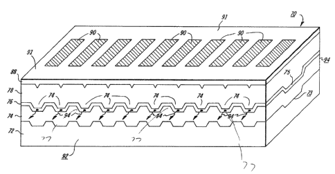
, configurations. The laser array 70 of Figure 3 is an example of one such
` ', configuration. Array 70 represents an extended multi-laser array of laser 10
.. ; shown in Figure 1. Laser array 70 comprises substrate 72 with cross-shaped
~' ~ 25 configuration 73 similar to the configuration 29 in Figure 1. Consecutively
~` I deposited on substrate 72 are cladding layer 74, active layer, single quantum
well layer or multiple quantum well layers 76, cladding layer 78 and contact
" layer 88. The configuration 73 is provided with a contiguous central gain
,i, guiding region 75 that extends transversely through the laser array with a
plurality of narrow index guiding regions 77 extending from the central
region 75 to either end facet 92 or 94. In this manner, a plurality of optical
cavities are formed as represented by the radiation emission outputs 77.
~.,
''''~ ~ .
. .1
,
.
,
.. . . . . . .
-
~ . ..
., , ~ .
. . . , ~
2 ~ ~ 7 0
; Each optica] cavity is pumped by means of a corresponding current
conf'inement region 90. Surrounding region 91 of at least the contact ]ayer
88 is rendered insulative by means of selective proton or ion implantment.
Also index guiding regions can be formed by means other than those
shown, such as Zn diffusion, chernical etching, preferential crystal growth or
other means known in ~e art. The inverse of this structure c~rl also be
formed. That is, the central laser region may be index guided with the outer
regions in the vicinity of the facet mirrors being gain guided. This
~;, configuration allows coupling of the ligh~ in the gain guided-sections for
o phase locked operation. By varying the length of the gain guided coupling
region single or rnultilobed phase-]ocked output beams can be obtained,
that is the phase can be controlled. Typical lengths of the gain guided
sections are in the range of 50-100 ,um.
:.
~' 15 Also, it should be evident that the array structure of Figure 3 may also
comprise a multiple emitter structure with each emitter having the the
geometry of laser 40 of Figure 2 wherein the index guding regions 32' and
34 of each array emitter en~ails this mesa geometly.
,
It should be understood that a single or multiple index guiding regions may
,, be provided in the central portion of a single laser array rather than the
ends with the ends formed as gain guiding regions. An illustration of a
~i single emitter is shown in the illustration of Figure 8 wherein the central
;~ index guiding region may be a channel or mesa index guiding region and
'' 1 25 the end regions 134 form gain guiding regions due to their large lateral
~,1 channel or mesa expanse.
.,
Figures 5-8 are illustrative of other combination gain/index guiding
'1 attributes for semiconductor lasers of the present invention. In each of the
configurations illustrated, the active region configuration is shown in cross-
'~ hatch with a dotted outline. The current confinement means is shown in
each illustration as extending from facet to facet, athough the confinement
.: . .
-:i
!
'.',
,,
. .
, .
.
.
. :., ~ . -
. .
~32~7~
~12-
may be limited to the gain guide region or regions of
each illustra-tion in the manner illustrated in Figure 1,
via selective proton or ion implantment or other current
confinement means. The configurations in each case may
comprise a channel configuration (like Figure 1) or a
mesa configuration (like Figure 2).
In Figure 5, the configuration 100 comprises narrow index
- guiding regions 102 and 104 between the end facets 101
and 103 and a gradually increasing or balloon shaped
..~
~" 10 central gain guiding region 106. The current confine-
ment means 105 may be narrower in width than the width
~-~ of index guiding regions 102 and 104. It should be
noted that the current confinement means may be narrow-
er or wider than the width of the index guiding means
in any of the configurations disclosed herein.
;,
"~J In Figure 6, the configuration 110 comprises a triangular
shaped gain guiding region 112 extending from end facet
~, 111 and coupled to a narrow index guiding active region
;~`; 114, which extends to end facet 113. The current con-
'"7 ' 20 finement region 115 is notably wider than the width of
' the index guiding active region 114.
: '1
'~1 In Figure 7j the configuration 120 comprises a periodic
'ri~ alternating configuration oF gain guiding regions 122
and index guiding regions 124. The configuration 120
ends at one facet 123 with a gain guiding region 122
i~; while at the other facet 121 it ends in an index guiding
region. However, the configuration could end at both
facets with either gain guiding region 122 or index
1 guiding regions 124. The current confinement means 125
`! 30 is shown to be wider than the width of index guiding
~ regions 124. The current confinement could alternatively
. .i .
.~'":
~...
:i
:. . .:, ,
: . - .
~, -
, - , . :
-12a- 1 3 2 ~ 670
:~ comprise a series of current confinement regions, each
I positioned over a single gain guiding region 124.
.~
. In Figure 8, the configuration 130 comprises a central
.~ rectangular index guiding region 132 with wide end
gain guiding regions 134 coupled to region 132 and each
end facet 131 and 133. The current confinement means
135 is shown to be wider than the width of index guiding
~ region 132.
;~ Although all the foregoing embodiments have been des-
` 10 cribed in connection
.:
':'
,; ~
~,,
~,
.
.
:`~
:!
: '`
. .
j
, 1
,, , : - -: :
'"' , :' ~ ; ~ ~ .: ' ' " '
. . !
~32~
- 13-
with semiconductor regimes comprising GaAs and (3aAlAs, other light
emitting regimes may be employed, such as lnGaAsP, GaAIP, GaAlSb, and
PbSnTe. Also, although the index guided geometries have been described in
terrns of channels and mesas, other means for obtaining lateral index guides
~`~ 5 such as selective diffusion, as in use of a "window stripe" laser, may be
used. Also, chemical etching and regrow~h, as in ~e case of a buried
` ~ heterostructure laser, as well as any other lateral index guiding scheme can
~ be used.
:
~' 10 As a specific example, the gain/index guided laser with a thin non-
absorbing mirror region that was grown and processed had the designation
M0739B PBB-81. The laser processed had the configuration of laser 40
shown in Figure 1. Several configurations were fabricated from a single
`i wafer in MO-CVD and consisted of an etched substrate channel patterns
`; 15 with index guiding regions 32 and 34 consecutively having 2, 4, 6 and 8 ,urn
widths. Aligned over each channel combination index guiding regions 32
~ and 34 were proton implanted strip geometry of consecutively respective
" widths 4, 6, 9 and 12 Jlm. Thus, a strip of correspondingly wider width was
positioned over a correspondingly narrower channel width. The laser facets
29 were coated with Al203 having a thickness equal to one half of the free
space wavelength output of the laser. The laser ~acet 28 was also coated with
a one half wavelength thick Al203 coating followed by a quarter wavelength
-~ thick coating of silicon for high reflectivity. Cleaves were made on the
; ~I processed wafer so that index guiding regions occurred adjacent to the end
2s facets while a gain guiding portion existed in the central gain guiding
, region. In addition, cleaves were made such tha~ the central region was
index guiding and the outer regions adjacent the facet were gain guided.
Further, c]ea~es were made so that one end of the laser was gain guided
:`' adjacent the cleaved facet and the other end was index guided adjacent the
; ~1 30 cleaved face~
~, An example of the results obtained is illustrated in Figure 14. The optical
,',~
.
!
.,
.~
' .
,. , . ~. ~
. . .
, : . . .
: . , ,. :-
. . . . . . ; . . -
`~ ~
~ 3 2 ~ 7 (3
output versus c~lrrent characteristics shown are fior an index/gain guide
laser 10 of Figure 1 having 6 ,um wide end channels and restricted current
confinement region 23. These results also showed stable single lobed far
~: field patterns with no near fie]d astigmatism when the index guiding regions
- s 32 and 34 were adjacent the end facets 27 and 28. In addition, multiple
longitudinal modes were observed as in a gain guided laser due to the
presence of region 30. Laser thresholds for all lasers were in the range of
90-130 mA. Laser operation was also obtained with the other mirror
configurations. Testing for transparency of the thinner active regions near
o the cleaved facets to the lasing light was also tested by making the contactstripe pattern end prior to the end facet. No Q-switching was observed, as is
.~ the case for the results in Figure 14, due to unpumped regions, these
. .
;l regions thereby indicating improved transparency of the thin regions near
the mirror facets.
While the invention has been described in conjunction with specific
embodiments, it is evident that many a]ternatives, modifications and
valiations will be apparent to those skil]ed in the art in light of the
~; foregoing description. Accordingly, it is intended to embrace all such
20 alternatives, modifications and variations as fall within the spirit and scope
of the appended claims.
.,
,,
.,,
:... 1 2.~i ~
~ "
`',
,,,,1 30
' ,~ !
.,
~ :i
~-,'''
.`'`i
~: ~` t
`i ~'`: ' , '` . '
`', ." . . ` ' '` '
:'.. ' '. ~
., ~ ` .
.: . .