Note: Descriptions are shown in the official language in which they were submitted.
1325~
BACKGROUND OF THE INVEN~ION
The present invent~ on relates generally to a method of
applying electrlcally conductiva printed patterns to electrically
insulating ~ubstrates. More particularly, the present invention
relates to a method of applying electrically conductive printed
patterns, particularly conductor patterns~ to electrically
insulating substrates, whereby a metal-containing coating agent
is transferred onto the ~ubstrate in an arrangement corresponding
to the printed pattern to be generated. The coating agent is
transferred under the influence of energy radiation, and is
chemically metallized. The present invention also relates to a
metal-containing coating agent for the appllcation of such
printed patterns to electrically insulating substrates.
German periodical "~alvanotechnik" 77 (1986) No. 1 t
pages 51 through 60, discloses a method for applying conductor
patterns to electrically conductive (SIC) substrates wherein the
transfer of the conductor pattern is undertaken with the
assistance of a laser. To this end, adhesive-coated epoxy resin
base material is employed as a substrate. This substrate is
subjected to pretreatment with S03 vapor phase etching with a NH3
etching stop for roughening the adhasive. A Cr (III)
photosensitizer which contains chrome (III)-chloride, sodium
oxalate and palladium ( II )-chloride, for example, is then applied
to *he substrate as a metal-containing coating agent. Pd nuclei
is generated in the region o~ the conductor pattern in the
ollowing laser image transfer, these Pd nuclei enabling a
chemical or galvanic thick copper-plating after a pre-
metallization with Ni-P and a haat treatmant at 100 to about
120C. Due to a thick copper-plati~g ln copper baths working
without external current and given lonyer exposition times,
- 2 - ~.
. - ,. , .. - , . - . - -
~3~7~
disociations of the adhesive layer from the base material can
occur so that the deposited interconnects lose thair adhesive
foundation.
"IBM Technical Disclosure Bulletin", VolO 15, No. 9,
February 1973, page 2855, discloses a method for applying
conductor patterns to ceramlc ~ubstrates. The method includes
applying to a green ceramic substrate a metal-contalning
thermoplastic powder that is subsequently exposed to a laser beam
ln accord with the desired conductor pattern. The laser beam
melts the thermoplastic powder embedding and adhering the metal
particles to the ceramic substrate. RPmaining metal-containing
powder that was not exposed to the laser beam can then be removed
with an air ~et.
These prior methods have not been entirely
satisfactory. In producing conductor patterns on a substrate,
numerous considerations must be taken into account. It is
desirable to reduce the exposition time. Further, it is
necessary for the electrically conductive pattern to be
sufficiently ~nchoredO Some previous methods of producing
conductor patterns on a substrate have not been entirely
satisfactory because they utilize decomposition raactions that
produce environmental pollution. Some previous methods of
producing these conductor pat*erns suffer the disadvantage of
being costly.
There is therefore a need for an improved method of
producing conductor patterns on a substrate, as well as an
improved metal~-contalning coating agent for the application of
such printed patterns of a substrate.
- 132~7~
20365-~779
SUMMARY OF THE INVENTION
The present invention provides an improved method for
applying electrically conductive printed patterns, particularly
conductor patterns, to electrically insulatlng substrates. The
method enables a simple transfer of the printed pa~tern and,
particularly in the manufacture of prin~ed circuit boards,
guarantees the production o~ extremely fine conductor structures
having an adequate adhesive foundation. The present invention
further provides a metal-containing coating agent suitable for
being applied to substrates to create a desired conductor pattern.
Thus, according to one aspect, the invention provides a
method for applying electrically conductive printed patterns to
insulating substrates wherein a metal-containing coating agen~ is
transferred onto a substrate under the influence of energy
radiation in a prlnted pattern to be produced and is chemically
me~allized, the coating agent includes a non metallic grainy
carrier substance having metal of the oxidation degree O applied
thereto.
According to another aspect, the invention provides a
metal-containing coating agent for applying electrically
conductive printed patterns onto electrically insulating
sub~trates comprising a non-metallic, grainy carrier to which is
applied metal in the oxidation degree 0.
--4--
~ 3 2 ~ 7 9 ~ ~0365-2779
According to still another aspect, the invention
provides a metal-containing coating agent for applying
electrically conductive printed patterns to electrically
insulating substrates comprising:
a non-metallic, grainy carrier substance consisting of at
least one compound chosen from the group consisting of:
activated carbon; conductive lampblack; calcium carbonate;
diatomaceous earth; bentonite; kaolin; silica gel; aluminum oxide;
titanium oxide; plastic; and pumice stone; and
a metal in the oxidation degree 0 that is applied to the
carrier substance, the metal consisting of a compound chosen ~rom
the group consisting of: precious metals; precious metal alloys;
and precious metal alloys with non-precious metals chosen from the
group consisting of zinc, nickel, tin, and copper.
In an embodiment of the present invention, the coating
material comprises a non-metallic, grainy carrier substance with
metal of the oxidation degree 0 applied thereon.
The present invention is based, in part, on the
discovery that the decomposition of metallo-organic compounds,
induced by energy radiation, can be avoided by employing metal of
the oxidation degree 0, insofar as the metal can be prepared in a
way that is suitable for the transfer of the printed pattern and
for the firm anchoring on or in the substrate. This preparation
of metal having the oxidation degree 0 ensues by utilizing a non-
metallic grainy carrier substance on which the metal is applied in
a finely distributed form. Such carrier substances for metals of
-~a-
` .
.. ..
~32~
20365-2779
the oxidation degree 0 are known and are referred to as carrier
catalysts which, for example, are utilized by hydration or
dehydration. In the manufacture of such carrier catalysts,
catalytic metals such as platinum, palladium, and nickel are
precipitated on ca~alyst carriers such as activated carbon,
diatomaceous earth, bentonite, kaolin, silica gel, aluminum oxide,
and pumice stone. Commercially available carrier
-~b-
~32~7~1
catalysts generally contain between approximately 0.5 to about 60
weight percent metal.
As a result of utilizing the coating agent of the
present inventlon, a three-dimensional d$stribution of the metal
nuclei is produced on the substrate. This three-dimensional
distribution promotes chemical metallization and considerably
reduces the exposition times in the corresponding baths working
without e~ternal current. Further, the grainy carrier substances
of the coating agent of the present invention afford a very good
anchoring in the substrate which is controllable through the use
of energy radiation. The anchoring guarantees an excellent
adhesive foundation for the interconnects in, for example, the
manufacture of printed circuit boards.
The present invention provides as a further advantage
reduced environmental pollution due to the elimination of the
previously required decomposition reactions. The present
inv~ntion also affords a more economical process for applying
electrically conductive printed patterns to substrates due to the
simplification of the process, and tha ability to proces~ the
coating material in liquid form. The ability to process the
coating material in liquid form is achieved because the metals
bonded to the carrier substances can be dispersed very well in
liquids and lead to stable liquid coa*ing agentsO
The present invention also provides a metal-containing
coating agent for applying electrically conductive printed
patterns, particularly conductor patterns to electrically
insulating substrates. The metal, in the metal-containing
coating, is in the oxidation degree 0 and is applie~ to a non-
metallic, grainy carrier substance. The above stated advantages
'. ~' !
2~7~
are achieved by employln~ the ooating agent of the present
invention in the pattern transfar with energy beams.
The method and ~oatin~ agent of the present lnvention
fundamentally enables ~ multltude of procesc$ng and transfer
forms. Thus, the ooating agent can be utilized ln Rolid form as
a powder wlth or without 2 bonding ~gent, in a llquld form, or in
the form of a foll to be applled to the surface of ~ ~ubstrate.
The foil can be composed only of tha coating agent or can be
composed of the coating agent and of sn auxiliary carrier. If a
foil ls used, the trans~er of the printed patterns with the foil
can proceed, for example, a set forth in French Published
Applicatlon No. 2 250 318.
Pursuant to the method of the present invention, the
printed patterns can be transferred, through the use of energy
radiation, in a variety of manners. In addition to the
utili~ation of masks, dies and the like, the printed patterns can
also be produced by relative movements between energy beam and
substrate. It should be noted that the term "trans~er of printed
patterns" includes the sur~ace-wide metallizations of
substrates. In this embodiment, subtractive techniques can also
be utilized.
Additional features and advantages of the present
invention are dascribed in, and will be apparent from, the
detailed description of the presently preferred embodiments and
from the drawings.
BREIF DESCRIPTION OF THE DRAWINGS
Figure 1 illustrates a ~chematic representation of an
embodiment of the method of the present invention.
:i .
, . . . . . . .
132~
~ lgure 2 illustrates a cross-sectional perspectlve view
of the coating agent of the present invention ~pplled to the
substrate.
~ igure 3 lllustrates a cross-sectional perspective view
of the substrate of ~igure 2 having the carrier substance of the
coating agent anchored therein.
Figure 4 illustrates a cross-sectional perspective view
of the conductor pattern transferred via the steps illustrated in
Figures 2 and 3 and anchored in the substrate.
~ igure 5 illustrates a cross-sectional view of the
conductor pattern of Figure 4 following a chemical and galvanic
metallization.
Figure 6 illustrates a cross-sectional perspective view
of an embodiment of the present lnvention wherein the ooating
agent contains a hot-melt adhesive as a bonding agent.
Figure 7 illustrates a cross-sectional perspective view
o~ the anchoring of the conductor pattern in the substrate of
Figure 6.
DETAILED DESCRIPTION OF THE PRESENTLY P~EFERRED EMBODIMENTS
The present invention provides an improved method for
applying electrically conductive printed patterns to insulating
substrates. The present invention also provides a coating
material for applying electrically conductive printed patterns *o
insulating substrates.
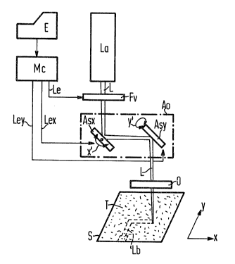
~ igure 1 illu-~trates a highly simplified, schematic
illustration of the present invention for transferring a
conductor pattern onto a substrate. The substrate S can be, for
example, composed of a thermoplastic synthetic. The illustrated
substrata S is a portion of the base material for an in~ection
molded printed circuit board. High-temperature-resistant
4'"~
~32~7~
thermoplastics such as, foF example, polyetherimide,
polyethersulfone, polyphenylene~ulfide, and li~uid crystal
polymers are particularly suitable às materials for such base
materials.
Pursuant to the method of the present invention, a
coating agent is applied to the surface o~ the substrate S. The
coating agent includes a gra~ny carrier substance T that is
indicated by tiny dots in Figure 1. In an embodiment of the
present invention, preferably, the coating agent is applied to
the surface of the substrate S in a layer thickness of
approximately 4 microns.
As illustrated, a laser ~a is utilized as an energy
beam. The laser La generates a laser beam L in whose beam path a
photographic shutter Fv, a first rotatable deflecting mirror Asx
of a deflection optics Ao, a second rotatable deflectin~ mirror
Asy of the deflection optics Ao, and an objective O are
successively arranged. The mirrors Asx and Asy function to focus
the laser beam onto the surface of the substrate S. The position
of the substrate S is determined with reference to a planar,
Cartesian x, y coordinate system. Accordingly, the first
deflecting mirror Asx of the deflection optics Ao functions to
deflect the laser beam L in the horizontal direction ~; this is
indicated in Figure 1 by arrows x'. The second deflecting mirror
Asy of the deflection optics ~o funct1ons to deflect the laser
beam L in the vertical dirsction y; this is indicated in Figure 1
by arrow y'.
To control the deflecting mirrors Asx and Asy, a
microcomputer Mc that has an input E is utilized. The
microcomputer Mc therefore determines the conductor pattern to be
produced on the substrater The lines for the control of the
- 8 -
132~7~
deflecting mirrors Asx and Asy are indicated by Lex and Ley,
respectively. The microcomputer Mc also ~ontrols the
photographic shutter Fv; this i~ $ndicated by a corresponding
line Le.
A variety of lasers La can be utilized ln the present
invention. For example, the laser La can be a C02 laser which is
utilized in continuous wave mode or which can also be
electronically pulsed, whereby the mean power lies between
approximately 0.5 watts to about 8 watts. The laser La can also
be, for example, a Nd-YAG laser having a mean power between
approximately 0.2 watts to about 50 watts. The focussing of the
laser beam L is adjustable, whereby the diameter of the laser
beam L at the substrate surface can be set to diameters of
between approximately 50 microns to about 400 microns.
For transferring the conductor pattern to the substrate
S, printing ink applied thereto is swept by the laser beam L, in
accord with the interconnect configuration lnput, into the
microcomputer Mc via the input E. The trace of the laser beam L
in the transfer of the conductor pattern is illustrated in Figure
1 as interconnect ~b. Further details of the transfer of
conductor patterns through the method of the present invention
will now be set forth in graater detail below with reference to
Figures 2 through 5.
Figure 2 ~llu~trates a hi~hly simplified, schematic
illustration of a substrate S on whose surface the individual
particles of the carrier substance T of the coating agent are
uniformly distributed. As illustrated, the coating agent
includes individual particles of metal M that are carried by the
surface of the carr1er substance T. Preferably, the carrier
substance T is: activated carbon; conductive lamp black; calcium
_ g _
`'- 'l~j _.
~2~
carbonate; diatomaceous earth; bentonite; kaolin; plastic; silica
gel; aluminum oxide; titinlum Gxide; or pumice stone - either
alone or in combi~ation. Preferably, the metal M i5 chosen from
the group of precious metals. In an embodiment, the metal is a
precious metal alloy with a non-precious metal selected from the
group consisting of: lead; ~inc; nickel; tin; and copper.
As stated above, a laser beam L is used to create the
conductor pattern on the substrate. To this end, the laser beam
L is guided over the sur$ace of the substrate S in the conductor
pattern desired to be produc0d. The laser beam L creates a
superficial melting of the substrate. As illustrated in Figure
3, this melting effects a securs anchoring of the carrier
substance T in the region of the desired conductor image.
After the meltiny by the laser beam L, non-anchored
carrier substancs T is removsd by brushing, spraying, or rinsing
in an ultrasound bath or the like~ Accordingly, as lllustrated
in Figure 4, only anchored carrier substance T in the region of
the conductor pattern to be produced remains on the substrate
S~ After removal of the non-anchored carrier substance T, the
particles of metal M, present in a three-dimensional distribution
on the anchored carrisr substance T, serve as nuclei for the
chemical metallization of the conductor pattern executsd without
external current. Therefore, the conductor pattern can be
completely constructed by chemical metal deposition or by
chemical and subseguent galvanic metal deposition.
Figure 5 illustrates the construction of the conductor
pattern by chemic~l and subsequent galvanlc mstal deposition. In
Figure 5, the chemically deposited metal is referenced by CM and
the galvanically deposited metal is referenced by GM. In an
embodiment of the present invention, preferably, copper is
-- 10 --
. ~ .
.
3~32~7~1
utilized for the chemically and galvanically deposited metals CM
and GM, respectively.
Figures 6 and 7 illustrate another embodlment of the
method of the present invention. In this embodlm2nt, the carrier
substance T is saturated with ~ hot-melt adhesive ~s the bond$ng
sgent. This bonding agent then melts under the influence of the
laser beam L and, as illustrated ln Fi~ure 6, leads to a gluing
of the carrier substance T to the surface of the substrate S.
In this embodiment, preferably a tharmoplastic synthetic
is again utilized as the substrate S. A heat-treatment can be
carried out after the removal of the unglued carrier substance
T. This he~t-treatment, as illustrated ln Figure 7, leads to a
fusing into the substrate surface and an even better anchoring of
the carrier substance T in the region of the desired conductor
pattern.
By way of example, microwaves can be used for the heat-
treatment step. Polar polymers having a high dielectric constant
have been found to function satis~actorily as the bonding a~ent
with microwaves. When polar polymers with a high dielectric
constant are utilized as the bonding agent, the microwaves will
only influence the substrate. Accordingly, with microwaves a
deformation of the substrate occasioned by the heat-treatment can
be reliably suppressed.
Preferably, the bonding agent comprises at least one
compound chosen from the group consisting of: polyamides;
polyimides; colophonium resins; hydrocarbon reslns; ketone
resins; polyvinylether; maleic resin; and polyvinyl buteral. In
an embodiment of the method of the present ln~ention, preferably,
polyamide and polyimide are utilized as the polar polymers for
the bonding agent to be treated with microwaves.
132~
By way o example, and not limitat~on, examples of the
method and coatin~ of the present invention will now be ~iven.
Example 1
A coatlng agent in accordance wlth the present invention
was made as follows. A carrier catalyst composed of activated
carbon hav~ng palladium applled thereto was utilized.
Approximately 10 weight percent palladium was distr$buted on
approximately 90 weight percent activated carbon. The activated
carbon having the palladium applled thereto was present in fine-
grained form. Approximately 30 percent of the grains had a grain
size below 10 microns; approximately 85 percent of the grains had
a grain size under 50 microns; and approximately 98 percent of
the grains had a grain size under 100 micronsO
The coating agent manufactured therewith contained the
following constituents: approximataly 30 weight percent activated
carbon plus palladium; approximately 2 weight percent yellow
pigment; approximately 25 to about 30 weight peroent bonding
agent; approximately 1.5 weight percent of a thix~troping agent;
and the remainder of the coating agent consisted of a solvent.
Although ethanol was used as the s~lvent, the solvent can include
at least one organic solvent chosen from $he group consisting
of: alcohols; esters; ketones; and hydrocarbons both aliphates
and aromatics. A mixture of maleic resin and polyvinyl butyral
was used as the bonding agent.
The coating agent described abovs, was applied to a
substrate of polyethersulphone by immers~on. The transfer of a
conductor pattern was carried out utilizing the process
illustrated in Figure 1 with the assistance of 8 laser beam.
Subsequently, the excess coating agent was removed in an
ultrasound cleaning bath utilizing isobutyl methylketone as the
- 12 -
.:~ ..,
11 32~7~
cleaning fluid. The conductor pattern was then built up through
copper depos~tion working without axternal current. The copper
was built up to a layer thickness of approxlmately 2 microns.
The conductor pattern was then built up through galvanlc copper
deposition, being built up therewlth to a layer thickness of
approximately 33 microns to produce an electrically conductive
prlnted pattern on the substrate.
Example 2
In this example, the steps and procedures ~et forth
above for example 1 were carried out except tha activated carbon
with the palladium applied thereto was replaced by a fin~r-
grained substance of carbon with palladium having a mean grain
size of about 4 microns. The resultant coating agent was then
applied to tha substrate by being sprayed on the substrate to a
layer thickness of approximately 4 to about 5 microns to produce
an electrically conductive printed pattern on the substrate.
Example 3
In this example, the steps and procedures set forth in
example 2 above were followed except calcium carbonate was
substituted for the activated carbon ln the evating agent.
Example 4
In this example, the steps and procedures set forth in
example 2 above were followed except the ratio of the activated
carbon to palladium in the coating agent was modified. Instead
of the weight ratlo of approximately 10 weight percent palladium
to approximately 90 wei`ght percent activated zarbon,
approximately 97 weight percent of activated carbon was utilized
as the carrier to approximately 3 weight percent of palladium.
- 13 -
.. . .
~32~7~
Example 5
In thi~ example, the steps and procedures set ~orth in
example 3 were followed, however, the weight ratio of calcium
carbonate to palladium was modificd. Instead of the weight ratio
of approximately 10 weight percent palladium to &pproximately 90
weight percent calcium carbonate, approximately 97 weight percent
of calcium carbonate served as the carrier for approximately 3
weight percent palladium.
Example 6
In this example, the steps and procedures of example 4
were followed except platinum was substituted for the palladium
used in the coating agent of example 4.
Example 7
In this example, tha steps and procedures of example 5
were followed except platinum was substituted for the palladium
used in the coating agent of example S.
Example 8
In this example, the steps of example 1 were followed,
however, after the removal of the excess coatlng agent an after-
treatment in an ammonia chloride bath was performed. This after-
treatment led to a significant improvement in the adhesion of the
interconnects to the ~ubstrate.
The after-treatment with a suitable bath can also be
utilized in the methods set forth in examples 2 through 7. In
utilizing the after-treatment with the steps and method of
example 2, the after-treatment with ammonia chloride led to an
adhesion of the interconnects of about 1 N/nm2.
Example 9
In this example, the steps and procedures of example 1
were followed, however, the activated carbon of the coating agent
,
~3~7~
was replaced by conductive-lampblack. Whereas irregularlties in
the interconnect ~tructure can occur when activated carbon is
utilized, when the grai~ is excessively large because of the
electrically non-conductive characteristic of the carbon, the
conductivity continues to exist at this location as a result of
the use of conductlve lampblack; even though the conductivity is
10ss than in the case of metals. The conductive lampblack thus
does not replace the metal. Rather, it augments the function of
the metals as nuclei for the following, ¢urrentless
metallization.
Example 10
In this example, the steps and procedures of example 1
were followed~ but the activated carbon of the coating agent in
example 1 was replaced by a plastic on an acrylate basis.
Example 11
In this example, the steps and proceduras of example 1
were followed, however, the activated carbon of the coating agent
was replaced by the plastic compound of the substrate. For
example, given a substrate and carrier composed of
polyetherimide, an extremely high adhes~on of the interconnects
to the substrate was achieved.
Example 1~
Following the steps and procedures of example 1, a
powdery coating agent composed only of the carrier catalyst,
i.e., of activated carbon and palladium, was used. This coating
agent was strewn onto the substrate, and was anchored with a
laser beam ln~accordance with the conductor pattern. The
substrate and coating agent was then chemically and, as needed,
galvanically copper-plated~ ~he soldering of the substrate was
thereby improved.
~32~7~
Example 13
In this example, the ~taps and procedures of example 1
were followed, however, the ooating agent was first applied to a
foil that served ~s ~n lntermadiate carrier. The foil was then
placed onto the substrate, whereupon the conductor pattern was
transferred onto the substrate through the foil with a laser.
Example 14
In this example, the steps and procedures of example 1
were followed, but, the activated carbon of the coating agent was
replaced by a plastic-bonded catalyst.
Example 15
In this example, the steps and procedures of example 14
were followed except a ground lon exchanger was used as a
plastic-bonded catalyst, a palladium (salt) solution having been
introduced thereinto and the palladium having been subsequently
chemically reduced to O-valent palladium.
Example 16
In this example, the steps and procedures of example 14
were follo~ed, but, a ground expanded polymer having a large
surface was used as a plastic-bonded catalyst, the palladium
having been deposited thereon. The expanded polymer to bs
utilized can e~ther be open-celled or closed-celled.
Example 17
In this example, the steps and procedures of example 14
were followed, but, a polymer-bonded palladium catalyst was used
as a plastic-bonded catalyst~ The palladium can be bonded
chelate-like or salt-like, such as polyamines or polyacrylic
acid, and can be reduced on the polymer to O-valent palladium.
The resultant product can still be subsequently soluble and can
then be applied to the substrate as a solution. If the resultant
~` ~3~7~
product is insoluble, it can first be ground and then be applied
to the substrate.
Sediment grlnding can be utilized for grinding the
plastics to form mlcron-sizad partlcles given the utilization of
plastic-bonded oatalysts. The polymers are then m$xed with an
inorganic ~alt. The polymers, due to electro-statlc charging,
would adhere to one another if the salt was not present. The
salt prevents the adheslon of the polymers to one another and is
in turn dissolved out with water after the grinding.
It should be noted that the anchoring of the conductor
pattArn on the substrate can be potentially enhanced through the
u5e of heat. For example, given the employment of substrates
composed of polyetherim~de, ~uch a tempering step performed after
the galvanic copper-plating increased the adhesion of tha
conductor pattern to the substrate by up to 50 percent.
It should be understood that various changes and
modifications to the presently preferred embodiments described
herein will be apparent to those skilled in the art. Such
changes and modifications can be made without departing from the
spirit and scope of the present lnvention and without diminishing
its attendant advantages. It is thereby intended that such
changes and modifications be covered by the appended claims.
, . .