Note: Descriptions are shown in the official language in which they were submitted.
~ 132~827
This invention relates to light sources and in
particular though not exclusively to optical transmitters.
Optical transmitters have an important
application in optical communications systems employing
optical fibres as transmission medium.
One of the major obstacles to the practical
implementation of optical communication systems is the
difficulty of achieving sufficiently accurate alignment in
and of the various system and subsystem components, and
maintaining that alignment for extended periods which may
be as long as the lifetime of the components.
The difficulty stems from the small dimensions of
the components concerned. Particularly where transmission
over single mode fibre is concerned, even minute
misalignments of the order of a micrometre or less can
cause noticeably increased transmission losses.
The active region of a typical semiconductor
laser is of the order of 2 ~m in cross-section. The core
of a single mode fibre is about 5 ~m to 10 ~m in diameter.
In a conventional laser transmitter, the active region
needs to be aligned with the fibre core. For practical
reasons it is often necessary also to space the end of the
fibre by a small distance, typically 20 to 25 ~m for a
lensed fibre end, from the adjacent laser face. This
reduces the required accuracy of alignment in practice to
about 1 to 2 ~m if excessive coupling losses between the
laser and the fibre are to be avoided.
~ 1325827
-- 2
A further alignment is usually required between
the back facet of the laser, that is to say the laser facet
opposite that facing the fibre, and a monitoring
photodetector. The usually much larger active area of the
photodetector, typically 250 ~m or more in diameter for a
slow speed monitoring device, relaxes the required accuracy
of alignment somewhat. However, light needs to be incident
on the active area from above (or below) the major plane of
the device. This is achieved conventionally by mounting
the photodetector with its major plane perpendicular to the
active region of the laser. This approach is adopted
despite the practical difficulties of handling a detector
device in that orientation during assembly, and finding a
satisfactory way of making electrical connections to the
photodetector, for example. Problems of this nature
adversely affect production costs, and present an obstacle
to high volume production in particular.
The present invention aims to provide an optical
transmitter assembly of a relatively simple structure which
readily lends itself to high volume production.
According to the present invention there is
provided an optical transmitting assembly comprising: an
optical source having an optical output coupled to pass
directly through a light refraction means towards a first
light output port, and an optical monitoring detector
arranged to receive scattered light output from the source
indirectly via at least one internal reflection of the
light refraction means and a second light output port,
wherein the source, the detector and the light refraction
means are mounted on a common support structure.
The light source will typically be a
semiconductor laser device, although in other applications
the light source may be a non-lasing device such as a light
emitting diode or an optical amplifier.
,"~
~,
~ 132~827
- 2a -
Conveniently, the light refracting means serve
the primary purpose of focusing light from the light source
into an optical fibre, or another recipient device.
132~827
- 3 -
Preferably, the refracting means comprise a lens
(which may be an element of a compound lens structure)
directly affixed to the monitoring detector. The lens is
advantageously a spherical lens. The lens may be arranged
relative to the source and the detector such that a portion
of the light passing through it is directed onto the photo-
detector by reflection, repeated reflection if necessary,
at the boundary of the lens.
Light may instead be directed onto the photo-
detector by light scatter in the lens material; frequentlyboth reflection and scatter mechanisms will be present.
In order to increase the amount of light reaching
the photodetector, the lens is conveniently mounted on the
detector by an adhesive with a refractive index greater
than that of air, thereby effectively extending the optical
contact cross-section between the lens and the
photodetector.
The support structure may conveniently be a
generally planar substrate, preferably of electrically
insulating, thermally conductive material. Any one or more
of the aforementioned components may be affixed directly to
the substrate or be affixed to subsidiary support
structures which are, in turn, affixed to or formed on the
common substrates.
The laser or other light source is conveniently
mounted with its light generating region, in the case of a
~; laser or an LED its active region, away from the support or
substrate, in contrast to many earlier arrangements where
the preferred arrangement was to mount the laser with its
active area nearest the substrate.
The photodetector is conveniently mounted on the
substrate such that the face affording entry of incident
light to its active area lies in a plane substantially
parallel with the mounting surface of the substrate.
The lens may be anti-reflection coated for high
performance devices to minimise reflections into the
optical source.
`- X
132~827
-- 4 --
In the case of an optical amplifier, lenses can
be similarly mounted on respective photodetectors at the
input and output ends to provide means for monitoring and
controlling the amplifiers.
The common substrate conveniently comprises a
monolithic block of electrically insulating but thermally
conductive material, the thermal conductivity being
required for dissipation of the heat generated in the light
source. Using an electrically insulating material permits
appropriate conductor tracks to be formed on the substrate,
by metal deposition for example.
The support structure may further provide surface
areas for anchorage points for an associated optical fibre,
control circuits, and the like.
The invention will now be described further by
way of example and with reference to the accompanying
drawings of which:
Figure 1 is a schematic perspective view of an
optical transmitter assembly;
Figure 2 is a side view of the assembly of Figure
1; and
Figure 3 is a side view of an optical amplifier
assembly.
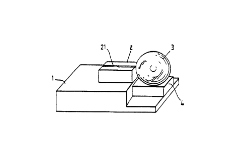
. Referring now also to Figures 1 and 2 of the
drawings, an optical transmitter assembly comprises a laser
2, a photodetector 4 and a spherical lens 3, all mounted on
a common stepped substrate 1. ~he substrate 1 is of a
material which is chosen to provide thermal dimensional
stability, and good heat conduction and electrical
insulation.
:~ The laser 2 may be any one of a variety of
: suitable semiconductor laser devices, the detailed
structure of the semiconductor device being largely
immaterial to the performance and understanding of the
present invention.
The approximate location of the active region of
the laser device is indicated schematically by the narrow
~ 1325827
-- 5 --
stripe 21. The laser 2 may be affixed to the substrate l
by soldering or in some other suitable manner which allows
heat conduction from the laser to the substrate and also
provides electrical continuity to appropriate conductor
tracks (not shown) on the top surface of the substrate 1.
In Figures 1 and 2 the laser is shown with its active
region uppermost; the laser may equally be mounted with the
active region nearest the substrate.
The optical output of the laser is coupled via a
lens 3 into an optical fibre (not shown) in the manner
described below.
As can be seen from Figure 2 in particular, the
laser 2 is mounted so that its active region 21 is remote
from, and extends parallel to, the top surface of the
substrate 1.
The photodetector comprises a planar photodiode
4 having its entry face in a plane parallel to the top
surface of the substrate 1. Instead of being a device with
a planar device structure the photodiode may have a mesa
structure, for example. The photodiode 4 is affixed to the
substrate 1 in a similar manner to the laser 2, with
electrical connection being made via the bottom surface of
the body of the photodiode 4 via a first conductor track
and by a bond wire from another conductor track to a
suitable bonding area of the photodiode 4. The photodiode
4 serves to monitor the total optical output of the laser
2 by receiving and sensing a portion of the optical output
of the laser 2, which portion of light is directed onto the
active area of the photodiode 4 via internal reflections
and/or scattering in the lens 3 as schematically
illustrated in Figure 2 by arrows 6b.
The lens 3 is a spherical lens of, for example,
sapphire or high refractive index glass with a refractive
index greater than 1.7. For many applications a refractive
index in the range 1.9 to 2.2 is the preferred. The
practical optimum value for the refractive index will vary
with the application concerned as it involves, for example,
132~827
-- 6 --
a trade-off between reflection from the lens surfaces and
the light-gathering ability of the lens. The dimensions of
the lens will typically be 200 to 500 ~m, although larger
(up to about 2 mm) and smaller (down to 150 ~m) lenses may
be used, if appropriate.
The lens 3 is affixed by means of adhesive 5 to
the top of the photodetector 4. The adhesive will
typically be a light curable adhesive; its refractive index
should be greater than the refractive index of the
surrounding air to allow not only light internally
reflected from the lens boundary, but also light scattered
within the lens, to be coupled into the photodiode 4.
The portion (6c) of optical power from the laser
2 which is incident on the entry face 41 of the photodiode
4, where it is converted into a corresponding electrical
output voltage appearing across tracks 43 and 44, is light
which would normally have been lost from transmission.
The present arrangement readily permits mounting
of the laser diode lO with its active region uppermost or
nearest the substrate. Mounting the laser diode with its
active region uppermost has, however, has several
significant advantages. Firstly, it avoids spurious
interference effects which can arise from the very narrow
virtual diffraction slit formed between the active region
21 and the surface 41 when the active region 21 is
immediately adjacent the surface 41. Secondly, mounting
the laser with its active region lowermost requires much
more accurate alignment between the front facet of the
laser and the corresponding edge of the substrate; if the
substrate projects beyond the laser, the aforementioned
interference effects will occur; if the laser overhangs the
substrate heat conduction away from the active area is
adversely affected leading to reduced device lifetime, or
lower reliability, or both.
Moreover, if the laser is affixed by soldering to
the substrate with its active region 21, nearest the
substrate, the formation of even a small solder bump may
132~827
-- 7 --
obstruct the light output of the laser and, again, cause
interference effects. Using the approach of the present
invention allows the laser 2 to be mounted with its active
area 21, uppermost, and hence not only largely avoids these
problems, but the use of the lens 3 further relaxes the
lateral alignment tolerances between laser and fibre. The
spacing of the lens 3 from the front facet of the laser is
typically a few ~m, depending upon the type of lens chosen
(eg whether the lens is a spherical lens, or a graded index
lens, etc).
By using a spherical lens, spurious reflection
from a cleaved fibre endface can be minimised by providing
a lateral and/or angular offset between the fibre and the
laser 2.
A further advantage of employing the arrangement
according to the present invention is that the laser can be
designed for 100% reflection at its back facet, resulting
in improved laser power output.
As shown in Figure 3, the invention may also be
applied to an optical amplifying device. Referring now to
Figure 3, the optical amplifier 102 shown there comprises
a laser-like semiconductor structure with an active region.
As before, knowledge of the operation of the device is
largely immaterial for an understanding of the present
invention. Briefly, unlike in the case of a laser, the
endfaces of the semiconductor structure are made non-
reflecting by application of an anti-reflection coating,
for example. Thus, no resonant cavity is formed and the
device is incapable of lasing, but can act like a
travelling wave amplifier for light incident upon it.
Undesirable reflection from the external lenses
3 and 103 can be largely avoided by ensuring that the axis
of the active region 121 does not intersect the lens
surface at right angles.
As in the case of the lens in Figures 1 and 2,
the photodiodes 4 and 104 can be connected to suitable
electronic circuits. By providing photodiodes at each end
~ 132~827
: - 8 -
of the amplifier which monitor input and output powers
respectively, amplifier parameters such as gain can be
readily controlled.
X