Note: Descriptions are shown in the official language in which they were submitted.
1 326072
AMPLIFICATION OF SIGNALS PRODUCED BY A
MAGNETIC SENSOR
Cross-Reference To Related Application
The present invention is related to the invention
described in the U.S. Patent No. 4,712,144 entitled
"Method and Apparatus for Reading Recorded Data by
Magnetoresistive Head", issued December 8, 1987 by
Klaas B. Klaassen and assigned to the assignee hereof.
The present invention is also related to the invention
described in U.S~ Patent No 4,706,138 entitled
"Amplification of Signals Produced by Magnetic Sensor",
issued November 10, 1987, by S. ~ove, et al and
assigned to the assignee hereof (hereafter reference
2).
Background of the Invention
Most existing magnetoresistive (MR) sensors,
including particularly sensors for bubble memories and
magnetic recording, are biased at a constant bias
current by preamplifiers which detect the signal
voltage developed at the sensor terminals. Since
stripe height is inversely proportional to sensor
resistance, and varies from sensor to sensor owing to
production variations and varies over the life of the
sensor in contact recording applications owing to wear,
it is desirable to detect signals produced by the
sensor which are independent of stripe height.
.,~
SA9-85-059
1 326072
Thus, it is desirab]e to detect and amplify a voltage
or a current representing ARIl/Rh, where ~Rh is the
change in MR sensor re~istance, Rh, arising from the
magnetic input signal from the media being read.
In U.S. Patent No. 4,706,138, issued November 10,
1987, by S. Jove, et al, enti-tled "Amplification of
Signals Produced by a Magnetic Sensor", a
transimpedance amplifier for biasing a magnetoresistive
sensor with a current having a constant time average
value, and for amplifying deviations from said constant
value produced by changes in the steady-state value of
sensor resistance, is described. DC feedback is used
to balance the current flow in both paths of a
d~fferential input stage to correct for DC offset
voltage which can otherwise develop at the output.
Summary of the Invention
According to the present invention, two
embodi~ents of an enhanced vo]tacle amplifier may be
used for constant voltage biaRing and amplifying the
signals produced by All MR sensor. In both circuits,
the differential input stage has built-in offset
correction derived from emitt:er resistors and a high
impedance current source. The circuits differ in
configuration of the transconcluctive feedback employed
to minimize the DC error Sigll~ l at the amplifier
OUtp~lt.
'Y~
SA9-85-059 2
- `` 1 326072
Electrically, the resistance, Rh, of the MR sensor is
disposed between the bases of a differential pair compris-
ing the input stage of the amplifier. The voltage which
biases the MR sensor is held constant because it is
provided independently of sensor resistance as the product
of the input stage emitter resistor and one-half of the
current from a constant current source.
In the circuit configurations of the present
invention, the signal representing ~ ~ /Rh is sensed as a
time-varying voltage across the MR sensor. The
steady-state value of Rh refers to the resistance value of
Rh while biased but not sensing magnetic field variations.
The input stage of the amplifier of the present
invention may be replicated as many times as there are MR
sensors in a given system. Ihe remaining components of
the amplifier comprise the output and feedback stages
which are common to all, and switched among, the input
stages in a multiple-head system. Additional circuitry
may be added to shorten setting time when MR sensors are
activated and deactivated in a multiple sensor system.
Description of the Drawing
Figs. lA and lB are block diagrams of the basic
concept of an amplifier constructed according to the
principles of the present invention.
SA9 ~5 059 3
1 326072
Fig. 2 is a circuit diagram of an amplifier
implemented according to Fig. lA.
Fig. 3 is a block diagram which shows the coupling of
selectable input stages to the common stage of the
amplifier.
Fig. 4 is a circuit diagram for the selectable input
stages of the amplifier of Fig. 3.
Fig. 5 is a circuit diagram for the common stage of
the amplifier of Fig. 3.
Fig. 6 is a circuit diagram of an amplifier
implemented according to Fig. lB.
Fig. 7A and 7B are circuit diagrams of enhancements
for reducing the settling time of the amplifiers of Figs.
5 and 6 when MR sensors are activated and deactivated in a
multiple-sensor system.
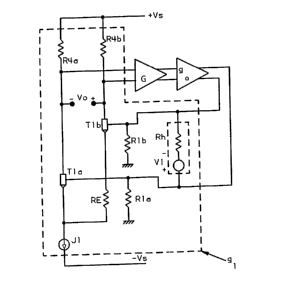
Description of the Preferred Embodi~e~t
Referring first to Figs. lA and lB, transistors Tla
and Tlb comprise a differential input amplifier stage
having built-in offset emitter resistor RE. Since Jl is a
high input impedance current source, this input stage
provides true differential signal processing for AC
signals. DC and low frequency error at the output, namely
SA9 85 05g 4
s 1 326072
at R4a and R4b, is minimized by feedback circuits in bo~h
configurations. The magnetoresistive sensor, shown as an
equivalent circuit comprising resistor Rh and voltage
source Vi, is coupled between the bases of transistors Tla
and Tlb.
In the configurations of Figs. lA and lB, the output
of the feedback stage, gO, is a current and the input to
the feedback is a voltage. Thus, the feedback amplifier
gO is a transconductance amplifier. An RC network is
incorporated into amplifier G in Fig. lA to provide a
dominant pole to separate low frequency error signals from
high frequency information signals. The error signal is
subtracted from the information signal, Vi, at the bases
of transistors Tla and Tlb.
When the error signal is minimized, current from
current source Jl is divided equally through transistors
Tla and Tlb to create a voltage reference, Vre, across
emitter resistor RE equal to the product of RE and
one-half of the current supplied by current source Jl.
Thus, Vre appears between the bases o:E transistors Tla and
Tlb and is therefore the voltage which biases MR sensor,
Rh, independent of the resistance value thereof.
In the configuration of Fig. lA, differential voltage
gain stage G couples the input differential stage
transistors Tla and Tlb to the transconductance amplifier
gO. In addition, as described elsewhere in this
SA9 85 059 5
1 326072
specification, gain stage G provides a dominant pole for
control of low frequency error signals. The DC voltage
across sensor Rh is kept constant independent of the value
of Rh by controlling the current therethrough. The
configuration of Fig. lA provides a ground potential at
the common connection of input resistors Rla and Rlb which
becomes the average potential of the MR sensor. If the
average potential of the sensor is ground, corrosion and
electrostatic discharge is reduced, and reliability of the
sensor is enhanced. However, the average potential of the
MR sensor could also be placed at any desired voltage with
this circuit.
In the configuration of Fig. lB, transconductance
amplifier gO comprises a single-ended, push-pull feedback
stage with a capacitor at the output. The current through
sensor Rh is controlled in the same manner as described
for the configuration of Fig. lA. Resistors Rla and Rlb
determine the amplifier input impedance and act as part of
the RC network in a resistor divider configuration with
sensor Rh. In the configuration of Fig. lB, capacitor C
also reduces noise associated with amplifier gO at
information signal frequencies.
Referring now to Fig. 2 with continuing reference to
Fig. lA, amplifier G comprises a differential voltage
follower and the input to transconductance stage gO.
Differential voltage follower includes transistors T3a and
T3b resistors R2a and R2b and current sources J3a and J3b.
SA9 85 059 6
1 326072
The input portion to the transconductance stage includes
transistors T4a and T4b, xesistors R3a and R3b, capacitor
C, and current source J4. The remainder of the
transconductance stage, gO, is a current mirror comprising
transistors Dla and Dlb, T2a and T2b, and current sources
J2a and J2b.
The general voltage gain transfer function of the
entire amplifier is given by
Equation (1)
~ 2 R4
2 C R32 Rb + Rh
- + RE + 2 rE
B _
15A = VO =
Vi R4 Rh B
1 1+-
s +
2 C R3 2 Rb + Rh _
_ + RE + 2 rE ib + B re
for Rl Rh and ft>>fpole
The terms for Equation (1) are defined as follows:
SA9 85 059 7
1 3 2 6 0 7 2
~b = series base resistance of T
B = forward current gain
rE = ( k T / q Ic1 ~
rb = series base resistance of T4 (includes R2)
re = ( k T / q Ic4 )
ft = device transition frequency
fpole= dominant pole frequency
Rh = MR head resistance (steady-state value)
Ic1 = collector current of Tl
Ic4 = collector current of T4
k = Boltzmann's constant
T = absolute temperature
g = electron charge
~he voltage gain transfer function at high freguencies is
given by:
Equation (2)
2 R4
Ai= for f ( 1 / (4 ~ C R3))
2 Rb + Rh
RE + 2 rE +
B
. .
The voltage gain transfer function at low freguencies is
given by:
SA9 85 059 8
1 3 2 6 0 7
Equation (3)
2 R4 ( rb + B re )
Az = A
2 Rb + Rh
s = O+ RE + 2 rE ~rb + B r ~ + B R4 Rh
Transfer functions (1), (2) and (3) are approximate
in that they do not consider the transition frequency of
transistors nor transistor forward current gain
variations. The amplifier has a high pass frequency
characteristic.
In order to facilitate switching from one MR sensor
to another in a multiple sensor system, the circuit of
Fig. 2 may be separated into a number of selectable input
stages, g1~ g2~ .... gn' each of which is dedicated to one
MR sensor. Such input stages are coupled to a common
stage, gc, as shown in Fig. 3.
Referring to Figs. 4 and 5, input stages g1 through
gn are coupled to common stage, gc, at nodes N1, N2, NF1
1 20 and NF2. Transistors T33 and T34 are coupled in cascode
i to extend the high fre~uency response when several input
stages are coupled to the common stage.
Common stage gO comprises the voltage follower stage
and the input to the transconductance stage of Fig. 2.
The RC network to form the dominant pole is located in
SA9 85 059 9
,.
ii 1 326072
common stage, g0, to reduce the number of capacitors
required. The RC network comprises capacitor C and
resistors R3a and R3b~ If resistors RSa, R5b, R5c and R5d
in Fig. 4 are equal and resistors are R6a, R6b, R6c, R6d,
R6e and R6f are equal, then the transconductance gain will
be the same as the gain for the amplifier of Fig. 2 if the
emitter area ratios of transistors Dla, Dlb, T2a, T2b, D6a
and D6b, T6a, T6b, T6c and T6d are equal and current
source J6 equals current source J4.
To select a desired input stage g1, current sources
JOA, J1, J5 and J6a must be simultaneously activated. The
deselected input stage is similarly deactivated by
deactivating corresponding current sources. Transistors
T6a and T6b correspond to current sources J2a and J2b of
Fig. 2. Current source J5, resistor R8 and transistors
D5 ! T5a, T5b and T7 are included to select the appropriate
current mirrors as different MR sensors are activated.
According to the present invention, feed forward
control is used to minimize the DC offset at the output of
the common stage while preserving low frequency
steady-state bandwidths. Referring to Figs. 4 and 5,
current from current source JOb is mirrored by the current
mirror comprising D16 and T2b and flows into one terminal
of Rh while current from current source JOa is drawn from
the other terminal of ~h. Thus, an offset current is
provided through Rh whose optimum value is given by
SA9 85 059 10
` 1 326072
Equation (43
dc Az [ (Jlt2) RE - J0 Rh]
Jl RE
where JO =
2Rh
With continuing reference to Figs. 4 and 5, the
current provided by current sources J6a and J6b are equal
during steady-state operation of the circuit. These
currents may be temporarily increased during switchover,
that is, when activating and deactivating input stages.
To control and reduce transient settling time of the
circuit, the currents from J6a and J6b are controlled by
an added control line to change the value of the current
at the moment of switchover. Thereafter, the sources may
be returned to their original value after transients have
been given a chance to settle. By increasing the current
available from current sources J6a and J6b, the current
available to charge or discharge capacitor C is thereby
temporarily increased and loop gain of the circuit is
correspondingly increased.
... .
Alternatively switchover transient recovery can be
controlled by using the feedback circuit configuration of
Fig. 7A. Operation of the circuit of Fig. 7A is described
in reference 2. Please note, nodes N3a, N3b, N4a, and
N4b, are coupled to the corresponding nodes of the common
stage of Fig. 5.
SA9 85 059 11
t 326072
The configuration of Fig. lB is implemented according
to the circuit of Fig. 6 wherein two selectable input
stages are shown. Block gO consists of a differential
voltage follower and a push-pull transconductance stage.
The differential voltage follower consists of transistors
T3a and T3b, resistors R2a and R2b and current sources J3a
and J3b. The push-pull transconductance stage comprises
an input stage and left and right current mirrors. The
input stage includes transistors T4a and T4b and current
source J4. The left current mirror includes transistors
Dlb, T2b, T27, T6 and resistors R5c, R5d, R6 and R28. The
right current mirror consists of transistors Dl and T2 and
resistors R5a and RSb.
The resistor divider network of Fig. lB is selectable
in the circuit of Fig. 6. The output of the
transconductance amplifier at node 5 is also the common
connection for the multiple resistor divider networks.
The desired divider network is selected simultaneously
with selection of the desired sensor/input-amplifier
combination. Thus, for example, if sensor Rha is desired,
transistors T29 and T31 are activated simultaneously by
applying the appropriate control signal at control node
"sel a", which simultaneously selects the desired divider
network and sensor/input-amplifier, respectively.
Similarly, if sensor Rhb is desired, an appropriate
control signal is applied at control node "sel b". For
the circuit configuration shown, the control signal
applied at either input node is a negative voltage.
SA9 85 059 12
`- 1 326072
The general voltage gain transfer function of the
amplifer of Fig. 6 is given by
Equation (5)
S ~+:~--C~ ]
Vo
A = _ =
Vi _ _ ,
2 R4 Rh B
s+ 1+ .
2 C Rl 2 Rb + Rh
L + RE + 2 rF [b + B r3
for ft >~ fpole where terms for Equation (5) are defined
elsewhere in the specification.
Voltage gain transfer function at high frequencies
for the circuit of Fig. 6 is given by
SA9 85 059 13
1 326072
Equation (6)
2 R4
ai = - for f ( 1 / ( 4~ C Rl )
2 Rb ~ Rh
+ RE + 2 rE
B
Voltage gain transfer function at low frequencies for
the circuit of Fig. 6 is given by
Equation (7)
A - A¦= 2 R ( rb + B re )
z 4
2 Rb + Rh
s 0 - + RE ~ 2 rE ~b + B r ~ + 2B R4 Rh
B
Transfer functions (5), (6) and (7) are approximate
in that they do not consider the transition frequency of
transistors nor transistor forward current gain
variations. The amplifier of Fig. 6 also has a high pass
frequency charactëristic.
As in the circuit configuration of Figs. 4 and 5,
feed-forward control is used to minimiæe DC offset at the
output. Current source J0 supplies an offset curxent
through the activated ~ . The optimum value of such
offset current may be estimated by the relation
SA9 85 059 14
-` ~; 1 326072
Equation t8)
dc Az [ ( Ic30/ 2 ) RE - JO Rh]
IC30RE
where Jo = - -where Ic30 = collector current of T30
2 Rh
In a manner similar to that for the circuit
configuration of Figs. 4 and 5, the transconductance
amplifier gain and the current available to charge or
discharge capacitor C can be increased to control
switchover transient settling time of the circuit. The
increase of gain and charge or discharge current is
provided in the same manner as previously described for
the circuit configurations of Figs. 4 and 5.
Alternatively, switchover transient recovery time can be
controlled by using the circuit of Fig. 7B, the operation
of which is described in reference 2. Nodes 5, 6A and ~B
are identified to indicate connection of this circuit at
correspondingly identified nodes of the circuit of Fig. 6.
SA9 85 059 15