Note: Descriptions are shown in the official language in which they were submitted.
1 326394
`LIGHT RECEIVING MEMBER HAVING IMPROVED
IMAGE MAKING EFFICIENCIES
FIELD OF THE INVENTION
This invention relates to a light receiving member
having improved image making efficiencies which is suited
for use in high-speed continueous image making systems
such as high-speed electrophotographic copying system,
high-speed facsimile system and high-speed printer system.
~,~
!BACKGROUND OF THE INVENTION
There have been proposed various kinds of a light
receiving member for use in electrophotography. Among such
known light receiving members, the public attention is now
focused on such light receiving members having a photo-
conductive layer formed of an amorphous material contain-
¦ing silicon atoms as the main constituent atoms ~herein-
after referred to as "A~Si") as disclosed in unexamined
Japanese Patent Publication Sho. 54(1979)-86341 and Sho.
56~1981)-83746 since said photoconductive layer has a
high Vickers hardness in addition to having an excellent
matching property in the photosensitive region in comparison
wlth that in other kinds of light receiving member and it
'."' ~ ' ~ :, ' '. '
1 326394
is not harmful to living things as well as man upon the use.
In concrete terms, said light receiving members have
a photoconductive layer constituted with an A-Si material
containing hydrogen atoms(H) and halogen atoms(X) [here-
inafter referred to as "A-Si(H,X)"] and a surface layer
being laminated on said photconductive layer which is
constituted with a high-resistance amorphous material
capable of allowing the transmittance of the light to be
used, which serves as a layer to effectively prevent the
photoconductive layer from being injected by electric
charge in the electrification process and which also serves
as a layer to improve the humidity resistance, deteriora-
tion resistance upon repeating use, breakdown voltage
résistance, use-environmental characteristics and durability
of the photoconductive layer.
There have been made various proposals on such surface
layer to be disposed on a photoconductive layer of a light
receiving member which exhibit the above mentioned functions
for the photoconductive layer.
And among those known surface layers, a surface layer
constituted with an A-Si(H,X) material containing at least
one kind atoms selected from carbon atoms(C), oxygen atoms
~0) and nitrogen atoms(N~ [hereinafter referred to as
"A-Sl(C,O,N)(H,X)"] in a relatively small amount is generally
evaluated as being the most preferred.
1 326394
However, for the light receiving members having any
of the known surface layers, even if it is the one that
has such preferred surface layer as above mentioned, there
are still unsolved problems particularly regarding the
allowances for the kind of an usable light source and
obtaining high quality images at high speed.
That is, firstly, it is extremely difficult to ef-
ficiently and mass-producing-like form the foregoing pre-
ferred surface layer to be of an uniform thickness and a
stable film quality and the resultant surface layer will
often become such that lacks uniformity of thickness and
homogeneity of the composition.
In addition, in any case, the light receiving member
having such surface layer is to be repeatedly used, for
instance, as in the case of electrophotographic copying
system. In that event, the surface layer will be gradually
rubbed out by the mechanical actions of a copying sheet,
toner, image developing device, cleaner etc. while being
accompanied with a locally partial abrasive force to there-
by result in becoming uneven in the thickness. These
problems relative to the layer thickness of the surface
layer in or to be in uneven state will often bring about
a local unevenness in the reflectivity on a light receiving
member in the ca~e where there exists such an interface
between the surface layer and the phtoconductive layer that
,- , .
:, , :
1 326394
, . .
` causes light reflection. This leads to making the light
receiving member defective in the photosensitivity and as
a result, the images to be formed will be of an uneven
image density which is a serious problem in electrophoto-
graphy.
~ Further, as it is required for the above surface layer
r to be highly resistive in certain respect, there will be
such occasion to invite generation of res~dual voltage in
thé case of using the light receiving member repeadedly,
particularly at high speed. In that case, there will be
caused a problem that because of said residual voltage,
the image quality will be reduced with the progress of the
repeating use of the light receiving member. And in the
case of using the light receiving member repeatedly for a
long period of time, there will be another problem relative
to the surface layer that its function to serve as a layer
to prevent the occurrance of defective images will be
gradually declined to thereby invite the occurrance of
defective images.
Further in addition, there are still another problems
even for such desirable light receiving member as having
the foregoing surface layer. That is, there will sometimes
be such occasion that reflected ray occurs on the surface
of the surface layer and another reflected ray occurs at
the interface between the surface layer and the
: ' , '
1 326394
photoconductive layer being situated thereunder. In that
case, the reflectivities of those reflected rays will be
sometimes largely changed in accordance with the wavelength
of the reflected ray, the layer thickness of the surface
layer and the refractive index of the surface layer that
results in bringing about unevenness in the color sensitivity
of the photoconductive layer and in making the resultant
images to be of uneven density.
The above problems relative to the surface layer were
not serious and could be disregarded for the conventional
ordinary-speed electrophotographic copying system but they
are weighty problems which are necessary to be settled in
order for such light receiving member to be made effectively
usable in high-speed continuous image-making systems such
as high-speed electrophotographic copying system using a
coherent light such as laser beam as the light source,
high-speed facsimile system and high-speed sprinter system
and especially, in digital high-speed continueous image-
making system.
There have been made the following proposals in order
to solve the foregoing problems with standing on the view-
points that the occurrence of relected ray at the interface
between the surface layer and the photoconductive layer is
to be ellminated by adjusting the refractive index of the
surface layer and that of the photoconductive layer at the
, . . ~ .
-
i 1 326394
.,
interface: (a) a manner of making the composition of the
surface layer to be closely resembled to or to be equivalent
to that of the photoconductive layer at the interface
between the two layers, (b) a manner of making the optical
band gap of the surface layer to be large enough in view of
making light to be effectively impinged into the photocon-
ductive layer and (c) a manner comprising combination of
the manners (a) and (b).
However, any of these manner is not reliable to obtain
such a desired light receiving member that can sufficiently
satisfy the requirement for the high-speed continueous
image-making systems, and there are still left some problems
to be solved, which are chiefly directed to residual images
and sensitivity related problems likely due to photocarrier
to be generated as a result of the occurrence of light
absorption at the interface between the surface layer and
the photoconductive layer.
Against this background, digital high-speed contineous
image-making systems gradually have come into wide use.
And there is an increased social demand for providing a
desirable light receiving member which can sufficiently
satlsfy the requirements for such digital high-speed con-
tinueous image-making systems and which can always and
stably exhibit the desired functions as the light receiving
member for said systems.
.
,
.
-
1 3263q4
SUMMARY OF THE INVENTION
This invention is aimed at eliminating the foregoing
problems in the conventional light receiving members for
use in electrophotography and providing an improved light
receiving member which can be effectively used in high-
speed continueous image-making systems without accompani-
ment of the foregoing problems and which can comply with
the aforementioned demands.
Another object of this invention is to provide an
improved light receiving member which can stably maintain
its original spectral sensitivity and which are free from
the foregoing problems relative to the ghost and the
sensitivity even in the case of continueously forming images
at high speed.
The present inventors have conducted extensive studies
for overcoming the foregoing problems on the conventional
light receiving members and attaining the objects as
described above and,as a result, have accomplished this
invention on the findings as below described.
That ls, the present inventors have experimentally
confirmed that the foregoing problems on the conventional
light receiving members are chiefly resulted from the
uneven state for the thickness of the surface layer which
is originated in the layer formation process, the unevened
state therefor which is caused by its repeating use and
,
,.
1 326394
the occurrence of reflected ray at the interface between
the surface layer and the photoconductive layer. And the
present inventors made further studies standing on the
viewpoint that a clue to the solution of the foregoing
problems will lie at the interface between the surface
layer and the photoconductive layer and while having due
regards also to the thickness of the surface layer.
As a result, the present inventors have found the facts
that there exist the following phenomena in relation to the
thickness of the surface layer, the refractive indexes of
the surface layer and the photoconductive layer, and the
layer quality and the photoconductivity of the surface layer.
That is, firstly, assuming the refractive index of the
surface layer to be n, the thickness of the surface layer
to be d, the wavelength of an incident to be ~, and m and
m' respectively to be an integer of 1, 2 or more, the
reflected ray becomes small when 2nd equals to (m-1/2)~
but it becomes large when 2nd equals m'~.
In concrete examples for the light receiving member
having a surface layer cons-tituted with an A-Si(H,X)
material containing at least one kind atoms selected from
carbon atoms, oxygen atoms and nitrogen atoms lhereinafter
referred to as "A-Sl(C,O,N)~H,X)"] of which refractive
index (n) is 2.0, when the incident ray is of 800 nm in
wavelength from semiconduGtor laser etc., the occurrence
;
. . . : ,
1 326394
of light reflection is scarce in the cases where the
thickness (d) of the surface layer is 1000 A, 3000 A and
. 5000 A respectively, but it comes to about 30% in the caseswhere the thickness (d) of the surface layer is 2000 A,
,` o o
4000 A and 6000 A respectively.
; Likewise, when the incident ray is of 550 nm (the
central value of visible light) in wavelength, the occurrence
of light reflection is scarce in the cases where the thick-
ness (d) of the surface layer is h90 A, 2060A, 3440 A or more
respectily, but it comes to about 30% in the cases where
the thickness (d) of the surface layer is 1380 A, 2750 A,
4130 A or more respectively.
Then, on the basis of these acknowledged phenomena,
~ it was found that in the convent~onal light receiving member,
s the reflectivity becomes large in some cases and small in
, other cases as the thickness of the surface layer becomes
large and these changes in the reflectivity (0%~30%) mainly
attribute to bring about the foregoing problems.
On the basis of the above findings, the present
inventors have come to obtain an acknowledge that the
foregoing problems on the conventional light receiving
members could be solved by eliminating or otherwise de-
creasing the occurrence of reflected ray at the interface
between the surface layer and the photoconductive layer
even in the case where the thickness of the surface layer
,,
.. . . . . .
~ l 3263q4
in a light receiving member is originally in uneven state
or in unevened state because of the repeating use.
On the basis of the above acknowledge, the present
inventors have tried to change the distributing states of
the constituents of the surface layer in a light receiving
member aiming at decreasing or eliminating the occurrence
of reflected ray at the interface between the surface layer
and the photoconductive layer.
That is, as a result of making studies in view of the
above on a light receiving member having a surface layer
constituted with an A-Si(C,O,N)(H,X~ material containing
a relatively large amount of at least one ~ind atoms
selected from carbon atoms (c), oxygen atoms (o) and nitrogen
atoms (N), there were found the following facts.
One of the findings is that when there are established
a high concentration layer region in the free surface side
of the surface layer and a low concentration layer region
in the photoconductive layer side of the surface layer for
at least one kind atom selected from carbon atom (c),
oxygen atom (o) and nitrogen atom (N) ~hereinafter referred
to as "the atom (C,O,N)" or simply "(C,O,N)"l and the
atom(C,O,N) ic incorporated so that the thicknesswise dis-
tributlng concentration of the atom(C,O,N) becomes discon-
tinueous, the matching between the refractive index of the
surface layer and that of the photoconductive layer become
.
i~
, . :
1 326394
. insufficient and the cordination among the refractive
indexes within the surface layer sometimes becomes also
insufficient to thereby bring about an unevenness in the
spectral sensitivity.
. Another finding is that when the atom(C,O,N) is
incorporated in the surface layer in the way that the
t distributing concentration be continueously changed in the
state of being small in the photoconductive layer side of
the surface layer but large in the free surface side of
the surface layer aiming at making the refractive index of
. the surface layer and that of the photoconductive layer
matched at the interface between the two layers and promot-
ing light to be impinged into the photoconductive layer,
although the occurrence of reflected ray at the interface
between the surface layer and the photoconductive layer can
be somewhat reduced, there is formed a undesired region
being inferior in the layer quality of which optical band
gap (Egopt) is undesirably narrow in the interface region
of the surface layer whereby photocarriers are generated
due to llght absorption in that region and they are con-
strained therein, that results in giving undesired influences
to the quallty of the resulting image.
Then, in due consideration of the above facts, the
present inventors have made another trial with respect to
the dlstributing state of the atom~C,O,N) in a surface
11
, ', ~' : ' : ~ . ~ - .
- . . ~ .. ~, ... . . ... ..
:
~ 1 3263q4
layer of a light receiving member in the way as shown in
Figure 2 as follows.
By the way, Figure 2 is a fragmentary sectional view
of a light receiving member in which are shown a photocon-
ductive layer 203, a surface layer 204, a free surface 207
and a interface 208 between the surface layer 204 and the
photoconductive layer 203. And in Figure 2, the oblique
full line shows the increasingly growing state of the
distributing concentration of the atom(C,O,N) in the surface
layer 204 and ~n stands for a refractive indes difference ~-
between the refractive index of the surface layer 204 and
that of the photoconductive layer 203 in the region in the
surface layer 204 which is adjacent to the interface 208
between the two layers.
That is, the present inventors have prepared a light
receiving member having a photoconductive layer constituted
wlth A-Si:H:X corresponding to the photoconductive layer
203 and a surface layer constituted with A-Si(C,O,N)(H,X)
corresponding to the surface layer 204 on an aluminum
cylinder, wherein the incorporation of the atom(C,O,N) into
the surface layer was conducted as follows.
That is, the atom(C,O,N) was incorporated in the
surface layer 204 in the way that its distributing concen-
tration is grown increasingly starting from the position
of the interface 208 leaving the refractive index difference
.
.. . . ~ . : .
.. ..
.
:. . - . . . : , ,- .
, .
,
1 3263q4
(~n) between the refractive index (n) of the surface layer
204 and the refractive index (np) of the photoconductive
layer 203 at the interface 208 between the two layers,
which can be disregarded in the image-making process,
toward the free surface 207 of the surface layer 204 as
shown in Figure 2. The resultant light receiving member
was examined and, as a result, it was found that the
occurrance of reflected ray at the interface 208 can be
extremely reduced; the foregoing various problems from the
relationships between the surface layer and the photocon-
ductive layer can be almost eliminated; and the light
receiving member can be desirably used in a high-speed
continueous image-making system since it always and stably
bring about high quality images in such high-speed con-
tinueous image-making system.
And the present inventors have acknowledged from the
results of the following Experiments 1 to 3 that the extent
of the above refractive index difference (~n) is indeed
important to obtain a desirable light receiving member
which is effectively usable in high-speed contineous image-
making systems such as high-speed electrophotographic
copying system, high-speed facsimile system, high-speed
printer system etc., and it is preferably ~n ~ 0.62 and
more preferably, ~n 5 0.4.
13
- ,: , . . ...
:
"
! ' . . . . ; ~ ' .
-
3263q4
, .
Experiment 1
The relations of the amount of the atom(C,O,N) to be
contained in the surface layer, the refractive index thereof
and the optical band gap were observed.
(1) Preparation of samples
For the purpose of measuring the refractive index and
the width of an optical band gap for a layer to be the
surface layer 204, layers having varied compositions of
silicon atoms(Si) and carbon atoms(c), layers having varied
compositions of Si and oxygen atoms(o) and layers having
varied compositions of Si and nitrogen atoms(N) were formed
on respective Corning's No. 7059 glass plates (product of
Corning Glass Works) using the conventional glow discharg-
ing film deposition apparatus.
In each case, the glass plate was placed on the surface
of the substrate holder in the deposition chamber and the
inner space thereof was adjusted to a vacuum of less than
10-7 Torr. And the glass plate was heated to a predetermined
temperature and maintained at that temperature. Thereafter,
film forming raw material gases were introduced into the
deposition chamber while controlling their flow rates.
After the flow rates of the film forming raw material gases
and the lnner pressure became stable, a discharge energy
was applied to thereby form a discharge plasma and to
deposit a film on the glass plate.
14
.
.
,
- -
.
~ 326394
As for the film forming period, it was so controlled
that the thickness of the film to be deposited will be
such that any error due to light absorption of the film
does not occur, any influence from the constituents of the
glass plate does not generate and a wavelength dependency
of the light absorption coefficient can be determined.
After a film having an appropriate thickness having
been formed on the glass plate, the power source was
switched off, the feedings of the film forming raw material
gases were stopped, the vacuum atmosphere in the deposition
chamber was released to atmospheric pressure then the glass
plate was cooled to room temperature. Thereafter the glass
plate having a deposited film thereon was taken out from
the deposition chamber.
(2) Observations
For each of the above prepared samples, the following
measurements were conducted.
(A) Measurement of the refractive lndex
For each of the A-Si:C film, A-Si:O film and A-Si:N
film respectively of 1 ~m in thickness, the transmittance
against a wavelength of 400 nm to 2600 nm was respectively
measured by using the conventional spectrophotometer
(product of Hitachi Ltd.).
The results were as shown in Figure 3(A).
By the way, as the transmittance will be periodically
.. , ,. ~ ....... :.
. . : . . , : . .:
.
.. . ..
. ' - ~, . . .
: - . . . . :
~ ~ . . .. . . .
1 326394
changed in accordance with the interference, the refractive
index is determined at the irreducible point (A) being
situated between the two points IB) and (C) where the
transmittance became 100~ in Figure 3(A).
And assuming the transmittance of the irreducible
point (A) to be T%, the following equation (1) can be
established between it and the refractive index. And in
accordance with the equation (1), the refractive index n
of each of the A~Si:C film, A-Si:O film and A-Si:N film
can be calculated.
n ~1~ng) 2
T/100 ={ 2 } .................................. (1)
n + ng
Wherein n is a refractive index of the A-Si:C film,
A-Si:O film or A-Si:N film and ng is the refractive index
(1.530) of Corning's No. 7059 glass plate.
(B) Measurement of the oPtical band gaP (EgoPt)
For each of the above samples A-Si:C film, A-Si:O
film and A-Si:N film, the absorbance against a wavelength
of 300 nm to 1000 nm was measured by using the foregoing
spectrophotometer. The results were as shown in Figure
3(B)-
Now, the following equation (2) can be establishedbetween the absorbance and the extinction coefficient of
each of the A-Si:C film, A-S1:0 film and A-Si:N film:
.
..
i` 1 3~63q4
:
d log e -------............................ (2)
Wherein D equals -log T, D stands for an absorbance,
`. e is 2.718281828... , d stands for the thickness of the
~ A-Si:C film, A-Si:O film or A-Si:N film and ~ stands for
c an extinction coefficient of the A-Si:C film, A-Si:O film
or A-Si:N film.
And the extinction coefficient can be calculated in
accordance with the above equation (2).
And the optical band gap can be determined by obtain-
ing an intersecting point of the following equation (3) with
x axis.
~hv = B(E~Eg) ............................... (3) ~ .
Wherein ~ is an extinction coefficient, h is Plank's constant,
~ is a frequency of the irradiated light, B is a proportional
constant, E i9 an energy of the irradiated light and Eg is
an optical band gap.
The equation(3) can be schematically explained as
shown in Figure 3(C).
(3) Results
The measurement results of the above (2)-(A) and
(2~-~B) are put together in Figures 3~D), 3(E) and 3(F).
17
. .
1 3263q4
In each of Figures 3(D), 3(E) and 3(F), the left
ordinate shows the optical band gap (Egopt)leV),
the right ordinate shows the refractive index (n) and the
abscissa shows the amount of the carbon atoms contained in
the A-Si:C film (C/Si~C)(.atomic %), the amount of the oxygen
atoms contained in the A-Si:O film (O/Si+O)(atomic ~), and
the amount of the nitrogen atoms contained in the A-Si:N
film successively.
From what are shown in Figures 3(D), 3(E) and 3(F),
the following facts can be acknowledged.
That is, when the arrival rate of light to the photo-
conductive layer is intended to heighten, the optical band
gap (Egopt) of the surface layer is larger as much as
possible the better. However, in the case of an amorphous
material containing silicon atoms, there is a tendency that
the refractive index (n) will become small as the optical
band gap (Egopt) increases.
In addition to this, the refractive index of the
A-Si(H,X) series photoconductive layer is about 3.2 to 3.5.
In this respect, it can be understood that the matching
between the refractive index of the surface layer and that .
of the photoconductive layer at the interface between the
two layers will become worse as the optical band gap (Egopt)
increases; and on the other hand, when the refractive index
~:
: . . ~ :: .
1 3263q4
of the surface layer is made to be matched with the
refractive index of the photoconductive layer at the inter-
face between the two layers, the optical band gap (Egopt)
in the photoconductive layer side region of the surface
layer becomes small accordingly whereby the light absorptive
proportion in the surface layer increases, the amount of
light to be impinged into the photoconductive layer reduces
and the photocarriers to be generated due to the light
absorption in the photoconductive layer side region of the
surface layer are constrained in that region to thereby
bring about problems leading to the occurrence of residual
voltage.
As a result of examining the ~n part shown in Figure 2
considering the relations of the optical band gap (Egopt),
the refractive index, and the amount of the carbon atoms,
oxygen atoms or nitrogen atoms shown in Figures 3(D), 3(E)
and 3(F) while having due regards to the above observations,
it was found that the supremum is preferably ~n S 0.62,
more preferably, ~n S 0.43 for the difference between the
refractive index of the interface region of the surface
layer with the photoconductive layer and the refractive
index of the photoconductive layer.
Experiment 2(1~
The relationship between the refractive index at the
.
::
.
''
-
1 32h~q4
interface between the surface layer and the photoconductive
layer and the image density difference was observed.
Firstly, there were provided ten 80 mm~ diameter
i aluminum cylinders (Samples Nos. 1 to 10) and another ten
108 mm~ diameter aluminum cylinders (Sample Nos. 11 to 20).
For the former ten cylinders of Sample Nos. 1 to 10,
a charge injection inhibition layer, a photoconductive
layer then a surface layer were formed continueously on
each of them using the conventional glow discharging film
deposition apparatus, wherein the formations of the charge
injection inhibition layer and the photoconductive layer
were carried out under the conditions shown in Table A and
the formation of the surface layer was carried out under
the conditions shown in Table B.
For the latter tem cylinders of Samples Nos. 11 to 20,
a long wavelength light absorptive layer (hereinafter
referred to as "IR absorptive layer"), a charge injection
lnhibition layer, a photoconductive layer then a surface
layer were formed continueously on each of them using the
conventional glow discharging film deposition apparatus,
wherein the formations of the IR absorptive layer, the
charge injection inhibition layer and the photoconductive
layer were carried out under the conditions shown in Table A
and the formatlon of the surface layer was formed under the
condltlons shown ln Table B.
.
.
. ~
IZ
-
1 326394
,a ~ O O O
~ ~ o o o
U~ ~
~q
tn
o
U ~ .
,.. ,, 1 o
.~ ~
U
O Q~
~f~ 1 a~
~o
o
O O o ~
~ Q
$
,4
O O O CD U~ O O CO U~ O O
O O
'~
~ .
'~ .
Id N -rl ai O N t~ O ~ t~
æ m ~ æ m
,P
P ~
g ~ . ,.
P~
zz 1 326394
a
O
,
V
s~ ~ O .
a) o
)
:- R f3
~ a~ o ,~
u~ ~ ~ 3 o
o ,~
.
,; a) o
. a
s~ ~ o
o U~ -~
,~ o
o
~ o~
o a~
0 3 ~
o ~
o
~q ~ o ~ ~,
a~ ~ ~
o
u~ 3 o
,~ o o ~:: ~ 3 a
2, ~`~ o ~ ,
~ 8 ~ o
!j rJ O L I
0~ 0~
9~ ~ 0
o 3 a~
a) ~ n 3
o
0
0 ~ ~
e
~ ~ 0 0
~ ln e ~
30 ~::
V,~
~o
.
:~ , : ,, , :
,
: . . .: : ,, , ~ . ,
.. . - , :
1 3~6394
For each of the thus obtained twenty samples (Samples
Nos. 1 to 20), the refructive index difference (~n) at the
interface between the surface layer and the photoconductive
layer and the image density difference (~D) were measured.
The ~n value was obtained in accordance with the same
procedures as in Experiment 1 using a refractive index
measuring sample which was prepared under the same conditions
as employed in Experiment 2 for measuring the refractive
index of the sample.
The measurement of the ~D for each of the samples was
conducted by setting each of the Samples Nos. 1 to 10 to
Canon's NP 755D electrophotographic copying machine
(product of Canon Kabushiki Kaisha) and each of the Samples
Nos. 11 to 20 to Canon's NP 9030 electrophotographic copying
machine ~product of Canon Kabushiki Kaisha) and by using
Eastman Kodak's standard gray scale chart.
The results of the measurements of the ~n and the ~D
for each of the Samples Nos. 1 to 20 were as shown in
Figure 4.
According to the results shown in Figure 4, it can be
apparently understood that the refractive index difference
(~n) between the refractive index of the surface layer and
that of the photoconductlve layer at the interface between
the two layers is preferably ~0.62, more preferably S0.43.
This confirms what were mentioned in Experiment 1.
~` 1 326394
Experiment 2(2)
The procedures of Experiment 2(1) were repeated, except
that the surface layer forming conditions were changed as
shown in Table C, to thereby form an IR adsorptive layer,
a charge injection inhibition layer, a photoconductive layer
and a surface layer on each of 80 mm~ diameter aluminum
cylinders (Sample Nos. 1' to 10') and each of 108 mm~ dia-
meter aluminum cylinders (Sample Nos. 11' to 20').
Table C
Discharg- Film form- Layer Substrate
Gasing Power ing speed thickness temperature
used (W) (A/sec.) (~)
Surface SiH4200 to 350 8 to 15 5000 280C
layer 2
(The changes in the composition ratios for the raw material
gases in the formation of the surface layer were conducted
by automatically controlling the flow rates of the raw
material gases along with a previously designed variation
coefficient carve by using a mass flow controller.)
For each of the thus obtained samples, the ~n and the
~D were measured by the same procedures as in Experiment
2~1). As a result, the same results as shown in Figure 4
were obtained.
24
~ '
,
- :
,
1 326394
Experiment 2(3)
The procedures of Experiment 2(1) were repeated, except
that the surface layer forming conditions were changed as
shown in Table D, to thereby form an IR adsorptive layer,
a charge injection inhibition layer, a photoconductive layer,
a surface layer on 80 mm~ diameter aluminum cylinders (Sample
Nos. 1" to 10") and 108 mm~ diameter aluminum cylinders
(Sample Nos. 11" to 20").
Table D
Discharg- Film form- Layer Substrate
Gas power sp~ed thickness temperature
used (W) (A/sec.)
H2
Surface siH4 200 to 8 to 15 5000 280C
layer NH3 300
..
(The changes in the composition ratios for the raw material
gases in the formation of the surface layer were conducted
by automatically controlling the flow rates of the raw
material ga6es along with a previously designed variation
coefflcient carve by using a mass flow controller.)
For each of the thus obtained samples, the an and the
QD were measured by the same procedures as in Experiment
2~1). As a result, the same results as shown in Figure 4
were obtained.
.
' ' '
- ~ , ., . . : . .
1 3263q4
Experiment 3
For each of the samples prepared in Experiments 2(1)
to 2(3) [Samples Nos. 1 to 20, Samples Nos. 1' to 20' and
Samples Nos. 1" to 20'']/ an optical band gap difference
(a Egopt) between the optical band gap of the surface layer
and that of the photoconductive layer and a sensitivity
(cm2/erg) were measured in addition to the measurement of
the an in Experiments 2(1) to 2(3).
The measurement of the aEgopt was conducted in
accordance with the procedures mentioned in Experiment 1,
and the measurement of the sensitivity was conducted in
accordance with the conventional sensitivity measuring
method which is widely employed in this technical field.
The results of the measurements were put together in
a three-dlmensional graph, and the values of the an, aEgopt
and sensitivity were read from said graph for each sample.
The results were as shown in Tables E(l) to E(3).
Wherein, there were used Sample No. 1 as the standard
for Samples Nos. 2 to 10, Sample No. 11 as the standard for
Samples Nos. 12 to 20, Sample No. 1' as the standard for
Samples Nos. 2' to 10', Sample No. 11' as the standard for
Samples Nos. 12' to 20', Sample No. 1" as the standard for
Samples Nos. 2" to 10", and Sample No. 11" as the standard
for Samples Nos. 12" to 20" to express the sensitivity of
each sample by a relatlve sensitivity.
26
;,
1 326394
It is a matter of course to say that any of those
samples used as the standard is satisfactorily usable in a
hlgh-speed continueous copying system.
'.:' . . . ~ . , ~ . . .. ~: ,
1 326394
Table E (1)
_
Sample No. ~ n ~ Egopt Relative sensitivity
80~ mm 108~ ~- Commonness 80~ mm 108
2 12 ~ I 1~ I 1~
3 13 0.3 1.30 1.20
4 14 0.43 0.47 1.30 1.2S
' .
0.5 0.52 1.30 1.30
6 16 0.62 0.57 1.30 1.30
,.'
7 17 0.85 0.67 1.30 1.30
8 18 1.05 0.72 1.30 1.30
. _ _ . ._
9 19 1.2 0.75 1.30 1.30
_ . ._ ..
0 20 1.3 0.77 1.30 1.30
28
'
,': ' ' . . . . . . .
. , ~.
.~
i 1 3263q4
Table E (2)
._
l Sample No. ~ n ~ E~opt Relative sensitivity
_
80 ~ mm 108 ~ mm Commonness Commonness 80 ~ mm 108 ~ mm
1' 11' O O 1.00 1.00
._ _ . ..
2 ' 12 ' 0.01 0.01 1.20 1.15
._
3 ' 13 ' 0.25 0.3 1.30 1.20
_
. 4 ' 14 ' 0.43 0.47 1.30 1.25
....
5 ' 15 ' 0.5 0.52 1.30 1.30
6 ' 16 ' 0.62 0.57 1.30 1.30
.. .
7 ' 17 ' 0.85 0.67 1.30 1.30
.
8 ' 18 ' 1.05 0.72 1.30 1.30
. ._
9 ' 19 ' 1.2 0.75 1.30 1.30
.
0 ' 20 ' 1.3 0.77 1.30 1.30
29
,: , --: :
, .
1 3 2 6 3 q 4
Table E (3)
~_
Sample No. ~ n ~ Egopt Relative sensitivity
t ._ __
, 80~ mm 108 ~ mm Commonness Commonness 80~ mm 1080 mm
`~c ._
,','. 1" 11" O O 1.00 1.00
.~ .
2 " 12 ~ 0.01 0.01 1.20 1.15
~ 3 " 13 0.25 0.3 1.30 1.20
,'1 __ ........................................ .. __
4 " 14 " 0.43 0.47 1.30 1.25
7 . .. _ .
~' 5 " 15 " 0.5 0.52 1.30 1.30
'7 _.__.
~ 6 " 16 " 0.62 0.57 1.30 1.30
, _ l
' 7 " 17 " 0.85 0.67 1.30 1.30
:'
8 " 18 " 1.05 0.72 1.30 1.30
.
ll 9 ....... 19 " 1.2 0.75 1.30 1.30
.. ...
0 " 2~ ~ 1.3 0.77 1.30 1.30
.
~ . .
1 326394
According to the results shown in Tables E(l) to E(3)
and the results shown in Figure 4, it can be apparently
understood that in the case where the ~n is made to be less
than 0.62 and the ~Egopt is made to be more than 0.01, the
image density difference becomes less than 0.05 and any of
such light receiving members excels in to giving a high
quality image formation and is accompanied with a superior
relative sensitivity.
What were above mentioned means that a light receiving
member having a surface layer constituted with A-Si(C,O,N)
(H,X) on a photoconductive layer constituted with A-Si(H,X)
series material of which the distributing concentration
state of the atom(C,O,N) is grown increasingly starting
from the position of the interface between the surface
layer and the photoconductive layer while leaving a portion
corresponding to a refractive index difference (~n) of
~n S 0.62 between the refractive index of the surface layer
and that of the photoconductive layer, which can be disregarded
in the image-making process, toward the free surface of the
surface layer is desirably suited for use in a high-speed
electrophotographic copying system ls that can exhibit
desired functions efficiently and effectively in a high-
speed contlnuous copying system.
The present invention has been completed based on the
above findings, and it provides an improved light receiving
~., ; , . ................................... .. .
, .. .
,
: .- : . . .
-
t` 1 326394
member having at least a photoconductive layer constituted
with A-Si(H,X) series material and a surface layer con-
stituted with A-Si(C,O,N)(H,X) for use in electrophoto-
graphy, etc. which is characterized in that the atom(C,O,N)
is contained in the surface layer in a state that the con-
centration of the atom (C,O,N) is grown increasingly starting
from the position of the interface between the surface
layer and the photoconductive layer while leaving a portion
corresponding to a refractive index difference (~n) between
the refractive index of the surface layer and that of the
photoconductive layer which can be disregarded in the image-
making process toward the free surface of the surface layer.
BRIEF DESCRIPTION OF THE DRAWINGS
Figures l(A) through l(C) are schematic cross-sec-
tional views illustrating representative embodiments of a
light receiving member to be provided according to this
invention;
Figure 2 is a schematic explanatory view for the state
of at least one kind atoms selected from carbon atoms,
oxygen atoms and nitrogen atoms to be contained in a surface
layer of the light receiving member according to this
invention;
Figure 3(A) is a schematic explanatory view for
~ . ,'' ' -,
.
1 326394
measuring the transmittance of a layer sample;
Figure 3(B) is a schematic explanatory view for
measuring the absorbance of a layer sample;
Figure 3(C) is a schematic explanatory view for
measuring an optical band gap of a layer sample;
Figure 3(D) is a graph showing the results of the
measurements of optical band gaps and refractive indexes
for layer samples containing silicon atoms and carbon
atoms;
Figure 3(E) is a graph showing the results of the
measurements of optical band gaps and refractive indexes
for layer samples containing silicon atoms and oxygen
atoms;
Figure 3(F) is a graph showing the results of the
measurements of optical band gaps and refractive indexes
for layer samples containing silicon atoms and nitrogen
atoms;
Figure 4 is a graph showing the relationships between
image density differences and refractive index differences
for layer samples;
Figure 5 is a schematic explanatory view of a fabrica-
tion apparatus for preparing a light receiving member
according to this invention;
Figures 6(A) through 6(L) are sehematic views
respectively illustrating the state of at least one kind
.
. .:
. ~
. t.~' 1 326394
"
atoms selected from carbon atoms, oxygen atoms and nitrogen
atoms to be contained in a surface layer of the light
receiving member according to this invention; and
Figure 7 is a schematic explanatory view of another
fabrication apparatus for preparing a light receiving
member according to this invention.
DETAILED DESCRIPTION OF THE INVENTION
Representative embodiments of the light receiving
member for use in electrophotography according to this
invention will now be explained more specifically refer-
ring to the drawings. The description is not intended to
limit the scope of this invention.
Representative light receiving members for use in
electrophotography according to this invention are as
shown in Figure l(A) through Figure l(C), in which are
shown substrate 101, charge injection inhibition layer 102,
photoconductive layer 103, surface layer 104, long wave-
length light absorptive layer (hereinafter referred to as
"IR absorptive layer") 105 and layer functioning as the
charge injection inhibition layer and also as the IR
absorptlve layer (hereinafter referred to as "multi-
functional layer") 106.
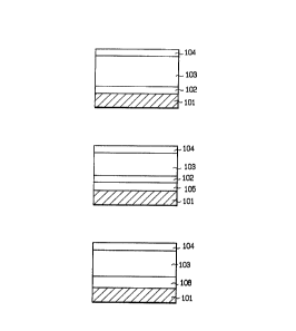
Flgure l(A) i8 a schematic view illustrating the
,,
, . . ,, ~,
,
.
1 326394
typical layer constitution of the light receiving member
according to this invention which comprises the substrate
101 and the light receiving layer constituted by the charge
injection inhibition layer 102, the photoconductive layer
103 and the surface layer 104.
Figure l(B) is a schematic view illustrating another
representative layer constitution of the light receiving
member according to this invention which comprises the
substrate 101 and the light receiving layer constituted
by the IR absorptive layer 105, the charge injection
inhibition layer 102, the photoconductive layer 103 and the
surface layer 104.
Figure l(C) is a schematic view illustrating another
representative layer constitution of the light receiving
member according to this invention which comprises the
substrate 101 and the light receiving layer constituted
by the multi-functional layer 106, the photoconductive
layer 103 and the surface layer 104.
Now, explanation will be made for the substrate and
each constituent layer in the light receiving member of
this invention.
Substrate 101
The substrate 101 for use in this invention may either
be electroconductive or insulative. The electroconductive
.
.. . . . .
1 326394
support can include, for example, metals such as NiCr,
stailess steels, Al, Cr, Mo, Au, Nb, Ta, V, Ti, Pt and Pb
or the alloys thereof.
The electrically insulative support can include, for
example, films or sheets of synthetic resins such as
polyester, polyethylene, polycarbonate, cellulose acetate,
polypropylene, polyvinyl chloride, polyvinylidene chloride,
polystyrene, and polyamide, glass, ceramic and paper. It
is preferred that the electrically insulative substrate is
applied with electroconductive treatment to at least one of
the surfaces thereof and disposed with a light receiving
layer on the thus treated surface.
In the case of glass, for instance, electroconductivity
is applied by disposing, at the surface thereof, a thin
film made of NiCr, Al, Cr, Mo, Au, Ir, Nb, Ta, V, Ti, Pt,
Pd, In203, SnO2, ITO (In203 + SnO2), etc. In the case of
the synthetic resin film such as a polyester film, the
electroconductivity ls provided to the surface by disposing
a thin film of metal such as NiCr, Al, Ag, Pv, Zn, Ni, Au,
Cr, Mo, Ir, Nb, Ta, V, Tl and Pt by means of vacuum
deposition, electron beam vapor deposition, sputtering,
etc., or applying lamlnation with the metal to the surface.
The substrate may be of any configuration such as cylindrical,
belt-like or plate-like shape, which can be properly
determlned depending on the application uses. For instance,
36
' ' ' ' ' ' . ''. '
.. . . . ..
...
.... . . ..
1 326394
in the case of using the light receiving member shown in
Figure 1 in continuous high speed reproduction, it is
desirably configurated into an endless belt or cylindrical
form.
The thickness of the support member is properly
determined so that the light receiving member as desired
can be formed.
In the case where flexibility is required for the light
receiving member, it can be made as thin as possible within
a range capable of sufficiently providing the function as
the substrate. However, the thickness is usually greater
than 10 ~m in view of the fabrication and handling or
mechanical strength of the substrate.
And, it is possible for the surface of the substrate
to be uneven in order to eliminate occurrence of defective
images caused by a so-called interference fringe pattern
being apt to appear in the formed images in the case where
the image making process is conducted using coherent mono-
chromatic light such as laser beams.
Charge Injection Inhibition Layer 102
The charge injection inhibition layer is to be disposed
under the photoconductive layer 103. And the charge
lnjection inhibition layer is constituted with an A-Si(H,X)
material containing group III element as a p-typ dopant or
, , . ,- :
. ~ , . .-.
.: -
- ~ . . . .
.--~
1 326394
.
group V element as an n-type dopant [hereinafter referred
. to as "A-Si(III,V):(H,X)"], a poly-Si(H,X) material con-
taining group III element or group V element [hereinafter
referred to as "poly-Si(III,V):(H,X)"] or a non-mono-
s crystalline material containing the above two materials
[hereinafter referred to as "Non-Si(III,V):(H,X)"].
The charge injection inhibition layer in the light
i receiving member of this invention functions to maintain an
electric charge at the time when the light receiving member
is engaged in electrification process and also to contribute
to improving the photoelectrographic characteristics of the
light receiving member.
In view of the above, to incorporate either the group
III element or the group V element into the charge injec-
tion inhibition layer is an important factor to efficiently
exhibit the foregoing functions.
Specifically, the group III element can include B
(boron), Al ~aluminum), Ga (gallium), In (indium) and Tl
(thallium). The group V element can include, for example,
P (phosphor), As (arsenic), Sb (antimony) and Bi (bismuth).
Among these elements, B, Ga, P and As are particularly
preferred.
And the amount of either the group III element or the
group V element to be incorporated into the charge injection
inhibition layer i8 preferably 3 to 5x10⁴ atomic ppm, more
38
: ' . ' ' ,''. ~ ,:,. : , `'
. . ~ , - . : ~. . .
: . : , . .
1 326394
preferably 50 to lx104 atomic ppm, and most preferably
lx102 to 5x10³ atomic ppm.
As for the hydrogen atoms (H) and the halogen atoms(X)
to be incorporated into the charge injection inhibition
layer, the amount of the hydrogen atoms (H), the amount of
the halogen atoms(X) or the sum of the amounts of the
hydrogen atoms and the halogen atoms (H~X) is preferably
lx103 to 7x10⁵ atomic ppm, and most preferably, lx103 to
2x10⁵ atomic ppm in the case where the charge injection
inhibition layer is constituted with a poly-Si(III,V):(H,X)
material and lx104 to 6x10⁵ atomic ppm in the case where
the charge injection inhibition layer is constituted with
an A-Si(III,V):(H,X) material.
Further, it is possible to incorporate at least one
kind atoms selected from oxygen atoms, nitrogen atoms and
carbon atoms into the charge injection inhibition layer
aiming at improving the.bondability of the charge injection
inhibition layer not only with the substrate but also with
other layer such as the photoconductive layer and also
improving the matching of an optical band gap(Egopt).
In this respect, the amount of at least one kind atoms
selected from oxygen atoms, nitrogen atoms and carbon atoms
to be incorporated into the charge injection inhibition
layer is preferably lx10-3 to 50 atomic %, more preferably
2x10⁻³ to 40 atomic ~, and most preferably 3x10⁻³ 30 atomic
~.
' . . ~ .~ ;'
- \
1 326394
The thickness of the charge injection inhibition layer
in the light receiving member is an important factor also
in order to make the layer to efficiently exhibit its
functions.
In view of the above, the thickness of the charge
injection inhibition layer is preferably 30 A to 10 ~m,
more preferably 40 A to 8 ~m, and most preferably, 50 A
to 5 ~m.
In the case where the charge injection inhibition
layer 102 is constituted with a poly-Si(O,N,C), the layer
can be formed by means of plasma chemical vapor deposition
(hereinafter referred to as "plasma CVD"). For instance,
the film forming operation is practiced while maintaining
the substrate at a temperature of 400 to 450C in a deposi-
tion chamber. In another example of forming said layer,
firstly, an amorphous-like film is formed on the substrate
being maintained at about 250C in a deposition chamber by
means of plasma CVD, and secondly, the resultant film is
annealed by heating the substrate at a temperature of 400
to 450C for about 20 minutes or by irradiating laser beam
onto the substrate for about 20 minutes to thereby form
said layer.
Photocondu tive Layer 103
The photoconductive layer in the light receiving
member according to this invention is constituted with an
.
I
. - , ,, " . , . -. : . .. ..
- .
: . - . .
1 326394
A-Si(H,X) material or a germanium (Ge) or tin(Sn) contain-
ing A-Si(H,X) material [hereinafter referred to as "A-Si
(Ge,Sn)(H,X)"l. The photoconductive layer 103 may contain
the group III element or the group V element respectively
having a relevant function to control the conductivity of
`the photoconductive layer, whereby the photosensitivity
of the layer can be improved.
-As the group III element or the group V element to
be incorporated in the photoconductive layer 103, it is
possible to use the same element as incorporated into the
charge injection inhibition layer 102. It is also possible
to use such element having an opposite polarity to that of
the element to be incorporated into the charge injection
inhibition layer. And, in the case where the element
having the same polarity as that of the element to be
incorporated into the charge injection inhibition layer is
incorporated into the photoconductive layer 103, the amount
may be lesser than that to be incorporated into the charge
injection inhibition layer.
Specifically, the group III element can include B
(boron), Al (aluminum), Ga (gallium), In (indium) and Ti
(thallium), B and Ga being particularly preferred. The
group V element can include, for example, P (phosphor), As
(arsenic), Sb (antimony) and Bi (bismuth), P and Sb being
particularly preferred.
.. , . ,. . . : ~ ,.... .
.: '.
-;. , : - : :-
~ . - : .
'' 1 3263q4
:
The amount of the group III element or the group V
element to be incorporated in the photoconductive layer
103 is preferably lx10-3 to lx103 atomic ppm, more pre-
ferably, 5x10⁻² to 5X10² atomic ppm, and most preferably,
lxlO-l to 2X10² atomic ppm.
The halogen atoms(X) to be incorporated in the layer
in case where necessary can include fluorine, chlorine,
r b~omine and iodine. And among these halogen atoms,
fluorine and chlorine are particularly preferred. The
amount of the hydrogen atoms(H), the amount of the halogen
atoms(X) or the sum of the amounts for the hydrogen atoms
and the halogen atoms(H+X) to be incorporate in the photo-
conductive layer is preferably 1 to 4xlO atomic %, more
preferably, S to 3xlO atomic ~.
Further, in order to improve the quality of the photo-
conductor layer and to increase it dark resistance, at
least one kind selected from oxygen atoms, carbon atoms
and nitrogen atoms can be incorporated in the photoconductive
layer. The amount of these atoms to be incorporated in the
photoconductive layer is preferably 10 to Sx105 atomic ppm,
more preferably 20 to 4x10⁵ atomic ppm, and, most preferably,
30 to 3x10⁵ atomic ppm.
The thickness of the photoconductive layer 103 is an
important factor in order to effectively attain the object
of this lnventlon. The thickness of the photoconductive
42
': ' . , ' ,'-' , ~,.' , . .:
~ ,~.: ,', . . ' ' : " " '
1 326394
layer is, therefore, necessary to be carefully determined
having due regards so that the resulting light receiving
member becomes accompanied with desired characteristics.
In view of the above, the thickness of the photocon-
ductive layer 103 is preferably 3 to 100 ~m, more preferably
5 to 80 ~m, and most preferably 7 to 50 ~m.
- Surface La~er 104
The surface layer 104 in the light receiving member
according to this invention has such special content as
previously detailed and makes a characteristic point of
this invention.
The surface layer 104 has a free surface and is to be
disposed on the photoconductive layer 103.
And, the surface layer 104 in the light receiving
member according to this invention contributes to improve
various characteristics commonly required ~or a light
receiving member such as the humidity resistance, deteriora-
tion reslstance upon repeating use, breakdown voltage
resistance, use-environmental characteristics and durability
of the llght receiving member, to reduce the reflection of
an incident ray on the free surface while increasing its
transmittance, and to reduce the absorption coefficient of
llght at the vicinal portion of the interface between the
surface layer and the photoconductive layer to thereby
43
' . , - ,
.. ~ .
1 3263q4
.
effectively decrease the density of a photocarrier to be
generated therein.
Further, in the case where the light receiving
member according to this invention is used as the electro-
photographic photosensitive member, the surface layer 104
contributes to significantly prevent the occurrence of
problems relative to the residual voltage and the sensitivity
which are often found on the conventional light receiving
member particularly in the case of the high-speed continuous
image-making process in addition to bringing about the
foregoing various effects.
The surface layer 104 in the light receiving member
according to this invention is constituted an A-Si material
containing at least one kind atoms selected from carbon
atoms(C), oxygen atoms(O) and nitrogen atoms(N) and, if
necessary, hydrogen atoms(H) and/or halogen atoms(X), that
is,A-Si(C,O,N)(H,X), and it contains at least one kind
atoms selected from carbon atoms(C), oxygen atoms(O) and
nitrogen atoms, that is, the atoms(C,O,N) in the particular
distributing state as previously detailed.
The amount of the atoms(C,O,N) to be contained in the
particular distributing state in the surface layer 104 is
the value which is calculated by the equation:
44
-: . .
: : ' '
1 326394
The amount of the atoms(C,O,N)]
[in the layer
-' -- - x 100
~The amount of The amount of
Si in the layer the atoms(C,O,N)
in the layer
Specifically, the amount of the atoms(C,O,N) can be
appropriately selected in the range between 0.5 atomic ~
for the minimum value and 95atomic % for the maximum value
respectively in the thicknesswise distributing concentra-
tion.
However, the mean value of the distributing concentra-
tion of the atoms(C,O,N) is preferably 20 to 90 atomic %,
more preferably 30 to 85 atomic %, and most preferably,
40 to 80 atomic ~.
The halogen atoms(X) to be incorporated in the surface
layer 104 in case where necessary can include fluorine,
chlorine, bromine and iodine. And among these halogen
atoms, fluorine and chlorine are particularly preferred.
The amount of the hydrogen atoms(H), the amount of the
halogen atoms(X) or the sum of the amounts for the hydrogen
atoms and the halogen atoms(HIX) to be incorporate in the
surface layer is the value which is calculated by the
following equation:
r The amount of HJ rThe amount of The amount of
~ln the layer , Lx in the layerJ ~tH~X in the layer
- x 100
rThe amount of l~The amount of + ~The amount of H 1
~Si ln the layerJ lthe atoms(C,O,N) l ln the layer
in the layer
.:
:, . . . .
: -
1 326394
Specifically, the amount of H, the amount of X or the
sum of the amount for H and the amount for X(H+X) is pre-
ferably 1 to 70 atomic %, more preferably 2 to 65 atomic %,
and most preferably 5 to 60 atomic %.
The thickness of the surface layer 104 in the light
receiving member of this invention is appropriately
determined depending upon the desired purpose.
It is, however, necessary that the thickness be
determined in view of relative and organic relationship in
accordance with the amounts of the constituent atoms to be
contained in the layer or the characteristics required in
the relationship with the thickness of other layer. Further,
it should be determined also in economical viewpoints such
as productivity or mass productivity.
In view of the above, the thickness of the surface
layer 104 is preferably 3x10⁻³ to 30 ~m, more preferably,
4x10⁻³ to 20 ~m, and, most preferably, 5x10⁻³ to 10 ~m.
IR AbsorPtiVe LaYer 105
The IR absorptive layer 105 in the light receiving
member of this invention is to be disposed under the charge
injection inhlbition layer 102.
And the IR absorptive layer is constituted with an
A-Si~H,X) material containing germanium atoms(Ge) or/and
tin atoms(Sn) [hereinafter referred to as "A-Si(Ge,Sn)
46
1 326394
.
(H,X~"], a poly-Si(H,X) material containing germanium atoms
(Ge) or/and tin atoms(Sn) [hereinafter referred to as
"poly-Si(Ge,Sn)(H,X)"] or a non-monocrystalline material
containing the above two materials [hereinafter referred
- to as "Non-Si(Ge,Sn)(H,X)"].
As for the germanium atoms(Ge) and the tin atoms(Sn)
to be incorporated into the IR absorptive layer, the amount
of the germanium atoms(Ge), the amount of the tin atoms(Sn)
or the sum of the amounts of the germanium atoms and the
tin atoms(Ge+Sn) is preferably 1 to 1x10⁶ atomic ppm, more
preferably lx102 to 9x10⁵ atomic ppm, and most preferably,
,! 5X10² to 8x10⁵ atomic ppm.
And, the thickness of the IR absorptive layer 105 is
preferably 30 A to 50 ~m, more preferably 40 A to.40 ~m,
and most preferably, 50 A to 30 ~m.
Multlfunctional LaYer 106
In the light receiving member of this invention, it
18 possible to make the above mentioned IR absorptive layer
to be such that can function not only as the IR absorptive
layer but also as the charge injection inhibition layer.
In that case, the object can be attained by incorporating
either the group III element or the group V element which
is the constituent of the aforementioned charge injection
inhlbition layer or at least one kind atoms selected from
47
, , -
-
1 326394
oxygen atoms, carbon atoms and nitrogen atoms into the
above IR absorptive layer.
As above explained, the light receiving member to be
provided according to this invention excels in the matching
property with a semiconductor laser, has a quick photo-
responsiveness and exhibits extremely improved electric,
optical and photoconductive characteristics, and also
excellent breakdown voltage resistance and use-environmental
characteristics, since it has a high photosensitivity in
all the visible light regions and especially excels in
photosensitive characteristics in the long wavelength
region.
Particularly, in the case of using the light receiving
member of this invention as the electrophotographic photo-
sensitive member, even if it is used in a high-speed con-
tinuous electrophotographic image-making system, it gives
no undesired effects at all of the residual voltage to the
image formation, stable electrical properties, high
sensitivity and high S/N ratio, excellent light fastness
and property ~or repeating use, high image density and
clear half tone and can provide a high quality image with
high resolution power repeatingly.
48
1 326394
Preparation of Layers -
The method of forming the light receiving layer of
the light receiving member will be now explained.
Each layer to constitute the light receiving layer of
i the light receiving member of this invention can be properly
prepared by vacuum deposition method u~ilizing the discharge
phenomena such as glow discharging, sputtering and ion
plating methods wherein relevant raw material gases are
selectively used.
These production methods are properly used selectively
depending on the factors such as the manufacturing conditions,
the installation cost required, production scale and properties
required for the light receiving members to be prepared.
The glow discharging method or sputtering method is suit-
able since the control for the condition upon preparing the
light receiving members having desired properties are
relatively easy, and hydrogen atoms, halogen atoms and other
atoms can be introduced easily together with silicon atoms.
The glow discharging method and the sputtering method may
be used together in one identical system.
Basically, when a layer constituted with A-Si(H,X) is
formed, for example, by the glow discharging method, gaseous
starting material capable of supplying silicon atoms(Si)
are lntroduced together with gaseous starting material for
introducing hydrogen atoms(H) and/or halogen atoms(X) into
49
1 326394
a deposition chamber the inside pressure of which can be
reduced, glow discharge is generated in the deposition
chamber, and a layer composed of A-Si(H,X) is formed on the
surface of a substrate placed in the deposition chamber
To from the layer of A-SiGe(H,X) by the glow discharge
process, a feed gas to liberate silicon atoms(Si), a feed
gas liberate germanium atoms, and a feed gas to liberate
hydrogen atoms(H) and/or halogen atoms(X) are introduced
into an evacuatable deposition chamber, in which the glow
discharge is generated so that a layer of A-SiGe~H,X) is
formed on the properly positioned substrate.
To form the layer of A-SiGe(H,X) by the sputtering
process, two targets (a silicon target and germanium
target) or a single target composed of silicon and germanium
is subjected to sputtering in a desired gas atmosphere.
To form the layer of A-SiGe(H,X) by the ion-plating
process, the vapors of silicon and germanium are allowed to
pass through a desired gas plasma atmosphere. The silicon
vapor is produced by heating polycrystal silicon or single
crystal silicon held in a boat, and the germanium vapor is
produced by heating polycrystal germanium or single crystal
germanium held in a boat. The heating is accomplished by
resistance heating or electron beam method (E.B. method).
To form the layer composed of an amorphous silicon
containing tln atoms (hereinafter referred to as "A SiSn(H,X)")
. . .
, . - . :
.
- : . - -
. . .. ,. . ~ .
1 326394
by the glow-discharge process, sputtering process, or
` ion-plating process, a starting material (feed gas) to
release tin atoms(Sn) is used in place of the staxting
material to release germanium atoms which is used to form
the layer composed of A-SiGe(H,X) as mentioned above. The
process is properly controlled so that the layer contains
a desired amount of tin atoms.
The layer may be formed from an amorphous material
namely A-Si(H,X) or A-Si(Ge,Sn)(H,X) which further contains
the group III element or the group V element, nitrogen
atoms, oxygen atoms, or carbon atoms, by the glow-discharge
process, sputtering process, or ion-plating process. In
this case, the above-mentioned starting material for
A-Si(H,X) or A-Si(Ge,Sn)(H,X) is used in combination with
the starting materials to introduce the group III element
or the group V element, nitrogen atoms, oxygen atoms, or
carbon atoms. The supply of the starting materials should
be properly controlled so that the layer contains a desired
amount of the necessary atoms.
If, for example, the layer is to be formed by the glow-
discharge process from A-Si(H,X) containing the atoms(O,C,N)
or from A-Si(Ge,Sn)~H,X) containing the atoms(O,C,N), the
starting material to form the layer of A-Si(H,X) or A-Si
(Ge,Sn)(H,X) should be combined with the starting materials
material used to introduce the atoms(O,C,N). The supply of
these starting materials should be properly controlled so that
51
. .
.
.
'' ,: : .; ~ ~ .
~ 1 326394
the layer contains a desired amount of the necessary atoms.
The surface layer in the light receiving member of
this invention is to be disposed on the photoconductive
layer and it is constituted with A-Si(C,O,N)(H,X) which
contains the atoms(C,O,N) in the special concentration
distributing state as previously detailed.
And the surface layer can be also properly formed by
vacuum deposition method utilizing the discharge phenomena
such as glow discharging, sputtering and ion plating method
wherein relevant raw material gases are selectively used.
For example, in order to form the surface layer using
the glow discharging process, it is possible to use a
mixture of a raw material gas containing silicon atoms(Si)
as the constituent atoms, a raw material gas containing
the atoms(C,O,N) as the constituent atoms and, optionally,
a raw material gas containing hydrogen atoms(H) and/or
halogen atoms(X) as the constituent atoms in a desired
mixing ratio, or a mixture of a raw material gas containing
silicon atoms(Si) as the constituent atoms and a raw material
gas containing the atoms(C,O,N) and hydrogen atoms(H) as
the constltuent atoms also in a desired mlxing ratio.
Alternatively, it is also possible to use a mixture
of a raw material gas containing the atoms(C,O,N) as the
constituent atoms and a raw material gas containing silicon
atoms(Si) and hydrogen atoms(H) as the constituent atoms.
. . . . ..
.
.
.
.. . . . . ... " .... .... .,. . ,. ~ .
.
. ~ ~ " , .: . .. ., .. -
i 1 326394
In the case of forming the surface layer by way of the
sputtering process, it is carried out by selectively using
a single crystal or polycrystalline Si wafer, a graphite
(C) wafer, SiO2 wafer or Si3N4 wafer, or a wafer containing
a mixture of Si and C, a wafer containing Si and SiO2 or a
wafer containing Si and Si3N4 as a target and sputtering
them in a desired gas atmosphere.
In the case of using, for example, a Si wafer as a
target, a gaseous starting material for introducing carbon
atoms(C) is introduced while being optionally diluted with
a dilution gas such as Ar and He into a sputtering deposi-
tion chamber thereby forming gas plasmas with these gases
and sputtering the Si wafer.
Alternatively, in the case of using Si and C as
individual targets, or in the case of using a single target
comprising Si and C in admixture, a single target comprising
Si and SiO2 in admixture or a single target comprising Si
and Si3N4 in admixture, a raw material for introducing
hydrogen atoms or/and halogen atoms as the sputtering gas
is optionally diluted with a dilution gas, introduced into
a sputtering deposition chamber thereby forming gas plasmas
and sputtering is carried out. As the raw material gas for
introducing each of the atoms used in the sputtering
process, those raw material gases to be used in the glow
discharging process may be used as they are.
53
' ,:
. ~ . . .
~` 1 3263q4
The conditions upon forming the surface layer con-
stituted with A-Si(C,O,N)(H,X)of the light receiving member
of this invention, for example, the temperature of the
substrate, the gas pressure in the deposition chamber and
the electric discharging power are important factors for
obtaining an objective surface layer having desired pro-
perties and they are properly selected while considering
the functions of the layer to be formed. Further, since
these layer forming conditions may be varied depending on
the kind and the amount of each of the atoms contained in
the light receiving layer, the conditions have to be
determined also taking the kind or the amount of the atoms
to be contained into consideration.
Specifically, the temperature of the substrate is
preferably from 50 to 350C and, most preferably, from 50
to 250C. The gas pressure in the deposition chamber is
preferably from 0.01 to 1 Torr and, most preferably, from
0.1 to 0.5 Torr. Further, the electrical discharging power
is preferably from 0.005 to 50 W/cm2, more preferably, from
0.01 to 30 W/cm2 and, most preferably, from 0.01 to 20
W/cm2 .
However, the actual conditions for forming the surface
layer such as temperature of the substrate, discharging
power and gas pressure in the deposition chamber can not
usually determlned with ease independent of each other.
54
,
, . . . .
., . ~ ~ ,, ~ . '
1 326394
Accordingly, the conditions optimal to the layer formation
are desirably determined based on relative and organic
relationships for forming the amorphous material layer
having desired properties.
The raw material for supplying Si in forming the
surface layer of the light receiving member of this
invention can include gaseous or gasifiable silicon hydrides
(silanes) such as SiH4, Si2H6,Si3H8,Si4Hlo, etc., SiH4 and
Si2H6 being particularly preferred in view of the easy
layer forming work and the good efficiency for the supply
of Si.
Further, various halogen compounds can be mentioned
as the gaseous raw material for introducing the halogen
atoms and gaseous or gasifiable halogen compounds, for
example, gaseous halogen, halides, inter-halogen compounds
and halogen-substituted silane derivatives are preferred.
Specifically, they can include halogen gas such as of
fluorine, chlorine, bromine, and iodine; inter-halogen
compounds such as BrF, ClF, ClF3, BrF2, BrF3, IF7, ICl,
IBr, etc.; and silicon halides such as SiF4, Si2H6, SiC14,
and SiBr4. The use of the gaseous or gasifiable silicon
halide as described above is particularly advantageous
slnce the layer constituted with halogen atom-containing
A-Si can be formed with no additional use of the gaseous
starting materlal for supplying Si.
:
- : :'' '
: , . .
1 326394
The gaseous raw material usable for supplying hydrogen
atoms can include those gaseous or gasifiable materials,
for example, hydrogen gas, halides such as HF, HCl, HBr, and
HI, silicon hydrides such as SiH4, Si2H6, Si3H6, and Si4010,
or halogen-substituted silicon hydrides such as SiH2F2,
SiH2I2, SiH2C12, SiHC13, SiH2Br2, and SiHBr3. The use of
these gaseous starting material is advantageous since the
content of the hydrogen atoms(H), which are extremely ..
effective in view of the control for the electrical or
photoelectronic properties, can be controlled with ease.
Then, the use of the hydrogen halide or the halogen-
substituted silicon hydride as described above is particularly
advantageous since the hydrogen atoms(H) are also introduced
together with the introduction of the halogen atoms.
The raw material to introduce the atoms(C,O,N) may be
any gaseous substance or gasifiable substance composed of
any of carbon, oxygen, and nitrogen.
Examples of the raw material to be used in or der to
lntroduce carbon atoms into the surface layer include
saturated hydrocarbons having 1 to 5 carbon atoms such as
methane~CH4), ethane(C2H6), propane(C3H8), n-butane(n-C4H10),
and pentane(C5N12); ethylenic hydrocarbons having.2 to 5
carbon atoms such as ethylene(C2H4), propylene(C3H6),
butene-1(C4H8), butene-2(C4H8), isobutylene(C4H8), and
pentene(CsH10)~ and acetylenic hydrocarbons having 2 to 4
.
c P 1 326394
carbon atoms such as acetylene~C2H2), methyl acetylene
(C3H4), and butine(C4H6)
Examples of the raw material to be used in order to
introduce oxygen atoms into the surface layer introduce
oxygen atoms~O) include oxygen (2) and ozone(O3).
f Additional examples include lower siloxanes such as
, disiloxane(H3SiOSiH3) and trisiloxane(H3SiOSiH20SiH3) which
are composed of silicon atoms(Si), oxygen atoms(O), and
hydrogen atoms(H).
Examples of the raw material to be used in order to -
introduce nitrogen atoms into the surface layer include
gaseous or gasifiable nitrogen, nitrides and nitrogen
compounds such as azide compounds comprising N as the
constituent atoms or N and H as the constituent atoms,
for example, nitrogen~N2), ammonia(NH3), hydrazine(H2NNH2),
hiydrogen azide(HN3) and ammonium azide(NH4N3). In addition,
nitrogen halide compounds such as nitrogen trifluoride(F3N)
and nitrogen tetrafluoride(F4N2) can also be mentioned in
that they can also introduce halogen atoms(X) in addition
to the introduction of nitrogen atoms(N).
~"
, '. , , , ' . ;,
:. .
1 3263q4
DESCRIPTION OF THE PREFERRED EMBODIMENTS
This invention will be described more specifically
while referring to Examples, but the invention is not
intented to limit the scope only to these examples.
Example 1
In this example, there was prepared an electrophto-
graphic photosensitive member in drum form for use in
electrophotographic copying system in which a hologen lamp
is used as the light source and a filter to cut a long
wavelength light is together used in order to rise the
color sensitivity.
In this example, the fabrication apparatus shown in
Figure 5 was used to prepare the above electrophotographic
photosensltive member.
Referring Figure 5, there is shown an aluminum cylinder
505' placed on a substrate holder 505 having a electric
heater 506 being electrically connected to power source
510.
The substrate holder 505 is mechanically connected
through a rotary shaft to a motor 504 so that the aluminum
cyllnder 505' may be rotated. The electric heater 506
surves to heat the alumlnum cylinder 505' to a predetermine
temperature and maintain it at that temperature, and it
also serves to aneal the depo~ited film. 508 stands for
58
~;i . ~ - . . : . : .
, . . . ~ .
,
:: , : ,. , , "
. .
1 3263~4
,
the side wall of the deposition chamber.
The side wall 508 acts as a cathod, and the aluminum
cylinder 505' is electrically grounded and acts as an anode.
High frequency power source 501 is electrically con-
nected through matching box 502 to the side wall 508 and
supplies a high frequency power to the side wall 508 as the
cathod to thereby generate a discharge between the cathod
and the anode.
507 stands for a raw material gas feed pipe having
upright gas liberation pipes 507', 507' respectively being
provided with a plurality of gas liberation holes to
liberate a raw material gas toward the aluminum cylinder
505'. 503 stands for exhaust system having a diffusion
pump and mechanical booster pump to evacuate the air in the
deposition chamber. The outer wall face of the deposition
chamber is protected by shield members 509, 509.
The other end of each of the raw material gas feed pipe
507 is connected to raw material gas reservoirs 561, 562 and
563. 551 through 553 are regulating valves, 541 through
543 are inlet valves, 531 through 533 are mass flow control~
lers and 521 through 523 are exlt valves.
An appropriate raw material gas is reserved in each of
the raw material gas reservoirs 561 through 563. For
example, there are reserved H2 gas in the gas reservoir 561,
silane (SiH4) gas in the gas reservoir 562, and a raw
59
.. . . .
~ `~
1 3263q4
:;
material gas for supplying C, O or N in the gas reservoir
563.
In this example, there was used an aluminum cylinder
of 358mm in length and:of 108mm in diam~ter as the substrate.
Now, prior to entrance of the raw material gases into
the deposition chamber, all the main valves of the gas
reservoirs were closed and all the valves and all the mass
flow controllers were opened.
Then, the related inner atmosphere was brought to a
vacuum of 10-7 Torr by operating the exhaust system 503.
At the same time, the electric heater 506 was activated to
uniformly heat the aluminum cylinder 505' to about 250C
and the aluminum cylinder was maintained at that temperature.
Thereafter, closing all the valves 521 through 523,
541 through 543 and 551 through 553 and opening all the main
valves of the gas reservoirs 561 through 563, the secondary
pressure of each of the regulating valves 551 through 553
was adjusted to be 1.5 kg/cm2.
Then, adjusting the mass flow controller 531 to 300
SCCM and successively opening the inlet valve 541 and the -
exit valve 521, H2 gas from the gas reservoir 561 was introduced
into the deposition chamber. At the same time, adjusting
the mass flow controller 532 to 200 SCCM and successively
opening the inlet valve 542 and the exit valve 522, SiH4 gas
from the gas reservoir 562 was introduced into the deposition
chamber.
.
,: , .
~ ~ . . . : . .
1 3263~4
After the inner pressure of the deposition chamber
became stable at 0.4 Torr, the high frequency power source
was switched on to apply a discharge energy of 200 W while
adjusting the matching box 502 to generate gas plasmas
between the aluminum cylinder 505' and the inner wall of
the deposition chamber.
This state maintained to form an A-Si:H layer of
25 ~m in thickness.
Successively, switching ofi the high frequency power
source 501, CH4 gas from the gas reservoir 563 was introduced
into the deposition chamber by the same procedures as in the
case of the H2 gas.
After the inner pressure became stable, the high
frequency power source 501 was switched on to apply a
discharge energy of 200 W, wherein the flow rates of each of
the H2 gas, SiH4 gas and CH4 gas were changed as shown in
Table F by adjusting the corresponding mass flow controllers
properly so that the distributing concentration state of
carbon atoms in the layer to be formed could be made in the
state as shown in Figure 6(A).
Table F
Gas used Initial 5tage Final Stage
H2 300 SCCM to 200 SCCM
SiH4 200 SCCM to 10 SCCM
CH4 50 SCCM to 290 SCCM
, ' :
- - .
~ . ~ : . : . -
.
:
` 1 3263q4
r
In this way, there was formed an A-SiC:H layer of
0.5 ~m in thickness on the previously formed layer.
Finally, switching off the high frequency power source,
closing all the valves, switching off the power source for
the heater, the aluminum cylinder was cooled to room
temperature under vacuum atmosphere and it was taken out
from the deposition chamber.
The thus obtained light receiving member was set to
modified Canon's electrophotographic copying machine NP7550
(product of Canon Kabushiki Kaisha) to conduct image making
on a paper sheet.
i Even when the machine was operated at a process
speed to output 100 A4 size paper sheets per a minute, every
processed paper sheet had high quality images without
accompaniment of any ghost and any uneven image density.
And, as an acceleration test under the above conditions,
when the above light receiving member was persisted using
toner containing abrasives, even after one million shots of
a A4 size paper sheet, there was not given any problem such
as uneven image density, ghosts etc. although there was
found a appreciable change on the thickness of the surface
layer.
62
:. . . .
i 1 326394
Examples 2 to 12
There were provided eleven aluminum cylinders which
are the same kind as used in Example 1.
The procedures of Example 1 were repeated, except that
the formation of a surface layer on the photoconductive
layer to be previously formed on each of the eleven aluminum
cylinders was so conducted that the distributing concentra-
tion state of carbon atoms in that layer could be made in
the state respectively as shown in Figures 6(B) to Figure
6(L) by automatically controlling the flow rates of SiH4
gas, H2 gas and C~4 gas, to thereby prepare eleven light
receiving members respectively having the surface layer of
0.5 ~m in thickness.
The resultant eleven light receiving members were
evaluated by the same procedures as in Example 1. As a
result, there were obtained satisfactory results on any of
them.
, . ', .
: . :
~` 1 326394
Examples 13 to 24
There were provided twelve aluminum cylinders, each of
which is 358 mm in length and 108 mm in diameter.
On the surface of each aluminum cylinder, a photocon-
ductive layer then a surface layer were formed under the
layer forming conditions shown in Table G to obtain twelve
light receiving members, wherein the changes in the flow
rates of SiH4 gas, H2 gas and CH4 gas were so made that the
carbon atoms distributing concentration state became
respectively as shown in Figure 6IA) to Figure 6(L) by
automatically controlling said flow rates using microcom-
puter.
The resultant twelve light receiving members were
engaged ln the same image-making test as in Example 1.
As a result, satisfactory results were obtained on ~ -
every light receiving member.
64
-, . - -
. 1 326394
o 8
S O r~ ~S
(D ~ 0 ~ti
~ ~ I'i y 1~.
., r~ ~4 (D
_r.1.~.
O O
r ~ ~
~ rr~ rl~
P m ~ m
S It ~P r~rS. R-
o, Y
4 ~
p ~D .
O ~ ~ ~
~. ~D O O o oo o o 1--
.4 , ,~o o oo 0
~ ~ ~ Q ~ D c
. o
~n . o
, .
N
' ~ ~
r.
~
o ~i P'
o
~q
O n ~t
m
:,: , , - . ~ . .. ...
, . : , , ~ . . .
1 326394
Examples 25 to 36
In each of Examples 25 to 36, there was prepared an
electrophotographic photosensitive member in drum form
having an IR absorptive layer, a charge injection inhibition
layer, a photoconductive layer and a surface layer for use
in laser beam printer in which a 80 ~m spot semiconductor
laser of 780 nm in wavelength is used as the light source,
using the fabrication apparatus shown in Figure 7.
The apparatus shown in Figure 7 is a modification of
the apparatus shown in Figure 5 that gas reservoir 664 for
NO gas, gas reservoir 665 for diborane diluted with H2 gas
(B2H6/H2), gas reservoir 666 for GeH4 gas, exit valves 624
through 626, mass flow controllers 634 through 636, inlet
valves 644 through 646 and regulating valves 654 through
656 were additionally provided with the apparatus shown in
Figure 5.
In every Example, an aluminum cylinder of 358 mm in
length and 80 mm in diameter was used as the substrate.
Each of the twelve light receiving members was prepared
as follows in accordance with the same procedures as in
Example 1.
That i8, after the related inner atmosphere of the
deposition chamber was brought to a predetermined vacuum
and the aluminum cylinder was heated to a predetermined
temperature, H2 gas, SiH4 gas,NO gas and GeH4 gas were
. . .
,
- ~.
: .
1 3263~4
introduced into the deposition chamber respectively at a
flow rate of 300 SCCM, 200 SCCM, 15 SCCM a~d 100 SCCM.
At the same time, B2H6/H2 gas was also introduced thereinto
at a flow rate corresponding to 3000 ppm as for B2H6 against
the SiH4 gas.
After the inner pressure became stable at 0.5 Torr,
a high frequency power energy of 200 W was applied to
thereby generate gas plasmas, whereby an A-SiGe:H:B:N:O
layer of 1 ~m in thickness to be the I~ absorptive layer
was formed on the aluminum cylinder. Stopping the introduc-
tion of the GeH4 gas, the above procedures were repeated
to thereby for an A-Si:H:B:N:~ layer of 5 ~m in thickness
to be the charge injection inhibition layer on the previous
layer.
Successively, stopping the introduction of the NO gas
and the B2H6/~2 gas, the above procedures were repeated to
thereby form an A-Si:H layer to be the photoconductive
layer on the charge injection inhibition layer.
Then, switching off the high frequency power source,
a surfa~e layer of 0.5 ~m in thickness containing carbon
atoms respectively in the carbon atoms distributing con-
centratlon state as shown in Figure 6~A) to Figure 6(L) on
the photoconductlve layer to thereby obtaln twelve light
receivlng members.
Each of the resultant twelve light receiving members
67
'
:, ., , :
. .
<
~ ~` 1 3263~4
was set to Canon's NP 9030 laser copier and the image-
making tests were conducted thereon by the same procedures
as in Example 1. As a result, satisfactory results were
obtained on every light receiving member as in Example 1.
. Examples 37 to 48
There were provided twelve aluminum cylinders which
i are the same kind as used in Example 1.
There were formed a photoconductive layer and a
surface layer on each aluminum cylinder to prepare a light
receiving member for use in electrophotography using the
apparatus shown in Figure 5.
For the photoconductive layer, carbon atoms were
incorporated into the layer aiming at improving the elec-
trification efficiency and the sensitlvity.
For the formation of the photoconductive layer in each
case, the procedures of Example were repeated, except that
SiH4 gas, H2 gas and C~4 gas were introduced into the
deposition chamber respectively at a flow rate of 200 SCCM,
300 SCCM and 1 SCCM, to thereby form a layer of 25 ~m in
thickness to be the photoconductive layer.
Then, in accordance with the procedures of Example 1
for the formation of the surface layer, a layer of 0.5 ~m
in thickness to be the surface layer was formed in each case
while incorporating carbon atoms into the layer in the carbon
68
, : .
:
'
' " ' ' : ' : ~ ,
. .
' " , ' ' ' ` ; , ' '
1 326394
atoms distributing concentration state respectively as shown
in Figure 6(A) to Figure 6(L) by regulatingthe flo~ r-ates of
SiH4 gas, H2 gas and CH4 gas under automatic control with
microcomputer.
The resultant twelve light receiving members were
evaluated by the procedures of Example 1.
' As a result, satisfactory results were obtained on
; every light receiving member as in example 1.
Example 49
In this example, there was prepared an electrophoto-
graphic photosensitive member in drum form for use in
electrophotographic copying system in which a halogen lamp
is used as the light source and a filter to cut a long
wavelength light is together used in order to rise the
color sensitivity.
As the substrate, an aluminum cylinder which is the
same kind as in Example was used.
On the aluminum cylinder, there were formed a photo-
conductive layer then a surface layer having a layer thick-
ness of 0.5 ~m which is composed with an A-Si:O:H.
The formation of the A-Si:O:H layer as the surface
layer was conducted by changing the flow rates of SiH4 gas
and 2 gas under the layer forming conditions shown in
Table H so that the obygen atoms distributing concentration
state in the layer became as shown in Figure 6(A)
69
: ., . . ~ . .
,
1 326394
?
Table H
Gas used Initital Stage Final Stage
i SiH4 200 SCCM to 50 SC~M
H2 300 SCCM 300 SCCM
2 5 SCCM to 50 SCCM
The resultant light receiving member was engaged in
the same image-making tests as in Example 1.
As a result, there were obtained satisfactory results
as in Example 1.
,~
Exam~_e 50
In this example, there was prepared a light receiving
member havlng a photoconductive layer and a layer composed
of A-Si:H:O:C to be the surface layer on the same kind of
' aluminum cylinder as in Example 1 in accordance with the
same procedures as in the case where the apparatus shown
in Figure 5 as above mentioned.
The formation of the A-Si:H:O:C layer as the surface
layer was conducted by changing the flow rates of SiH4 gas,
2 gas and CH4 gas under the layer forming conditions shown
~; in Table I so that the dlstributlng concentratlon states of
the oxygen atoms and the carbon atoms ln the layer became
as shown in Figure 6~A).
. . . .. .
~-. ., , ~ -
.- . . . , -
,............................ ~ . : .:
- -
1 3263q4
Table I
Gas used Initial Stage Final Stage
H2 300 SCCM 300 SCCM
.. SiH4 200 SCCM to50 SCCM
2 2 SCCM to10 SCCM
CH4 3 SCCM to40 SCCM
The resultant light receiving member was enyaged in
the same image-making tests as in Example 1.
As a result, there were obtained satisfactory results
as in Ex~mple 1.
Example 51
In this example, there was prepared a light receiving
member having a photoconductive layer and a layer composed
of A-Si:H:F:O to be the surface layer of 0.5 ~m in thick-
ness on the same kind of aluminum cylinder as in Example 1
in accordance with the same procedures as in the case
where the apparatus shown in Figure 5 as above mentioned.
The formation of the A-Si:H:F:O layer as the surface
layer was conducted by changing the flow rates of SiH4 gas,
SiF4 gas and 2 gas under the layer forming conditions
~hown in Table J 80 that the distributing concentration
state of carbon atoms in the layer became as shown ln
Flgure 6(A).
,. , . ~ , .' " :., -'; ' -
.: .
.. . . . .
1 326394
Table J
Gas used Initial Stage Final Stage
; H2 300 SCCM 300 SCCM
SiH4 150 SCCM to 30 SCCM
SiF4 50 SCCM to 20 SCCM
2 5 SCCM to 50 SCCM
The resultant light receiving member was engaged inthe same image-making tests as in Example 1.
As a result, there were obtained satisfactory results
as in Example 1.
Example 52
In this exampleJ there was prepared a light recei~ing
member having a photoconductive layer and a layer composed
of A-Si:H:F:O:C to be the surface layer of 0.5 ~m in
thickness on the same kind of aluminum cylinder as in
Example 1 in accordance with the same procedures as in the
case where the apparatus shown in Figure 5 as above mentioned.
The formation of the A-Si:H:F:O layer as the surface
layer was conducted by changing the flow rates of SiH4 gas,
SiF4 gas, 2 gas and CH4 gas under the layer forming condi-
tions shown in Table K so that the distributing concentra-
tion states of oxygen atoms and carbon atoms in the layer
became as shown in Figure 6(A).
.
,: ,. ' ' . :
1 326394
Table K
Gas used Initial Stage Final Stage
H2 300 SCCM 300 SCCM
SiH4 150 SCCM to30 SCCM
. SiF4 50 SCCM to20 SCCM
2 2 SCCM to10 SCCM
,~ CH4 3 SCCM to40 SCCM
The resultant light receiving member was engaged in
the same image-making tests as in Example 1.
As a result, there were obtained satlsfactory results
as in Example 1.
Exam~le 53 to 63
There were provided eleven aluminum cylinders which
are the same kind as used in Example 1.
There were formed a photoconductive layer and a surface
layer on each aluminum cylinder to prepare a light receiving
member for use in electrophotography using the apparatus
shown in Figure 5.
The formation of the surface layer for each of the
eleven light receiving members was conducted in accordance
wlth the procedures of Example 1.
That i8, the flow rates of SiH4 gas and 2 gas were
automatically changed using microcomputer so that the
distrlbuting concentration state of oxygen atoms in the
- . ~ .
1 326394
layer became respectively as shown in Figure 6(B) to
Figure 6(L), whereby a layer composed of A-Si:O:H to be the
surface layer was formed in respective cases.
; The resultant eleven light receiving members were
engaged in the same image-making tests as in Example 1.
As a result, there were obtained satisfactory results
on every light receiving member as in Example 1.
E~ to 75
There were provided twelve aluminum cylinders which
are of the same kind as used in Example 1.
In each case of Examples 64 to 65, there were formed
a charge injection inhibition layer, a photoconductive
layer and a surface layer in this order on the surface of
the aluminum cylinder under the layer forming conditions
shown in Table L using the apparatus shown in Figure 7.
In the for~ation of the surface layer, the flow rates
of SiH4 gas and 2 gas were automatically changed using
microcomputer so that the distributing concentration state
of oxygen atoms in the layer became respectively as shown
in Figure 6(A) to Figure 6~L), whereby a layer composed of
A-Si:O:H to be the surface layer was formed in respective
cases.
The resultant light receiving member was engaged in
the same image-making tests as in E~ample 1.
74
~:
- . ~
1 326394
As a result, the.re were obtained satisfactory results
as in Example 1.
Table L
Discharging Layer
Name of Gas Flow rate power thickness
layer used (SCCM) (W) (~m)
Charge SiH4 200
injectionH2 300 3.0
inhibitionB2H6/H2 1000 to
layer 0 ppm(B2H6)
Photoconductive SiH4 200 200
layer H2 300 22
Surface layer SiH4 200 to 50
H2 300 1.0
2 5 to 50
Temperature of substrate: 250C
Discharging power frequency: 13.56 MHz
Examples 76 to 87
There were provided twelve aluminum cylinders which
are of the same kind as used in Example 1.
In each case of Examples 76 to 87, there were formed
a charge injection inhibition layer, a photoconductive layer
and a surface layer in this order on the surface of the
aluminum cylinder under the layer forming conditions shown
in Table M using the apparatus shown in Figure 7.
In the formation of the surface layer, the flow rates
1 326394
of SiH4 gas and 2 gas were automatically changed using
microcomputer so that the distributing concentration state
of oxygen atoms in the layer became respectively as shown
in Figure 6(A) to Figure 6(L), whereby a layer composed of
A-Si:O:H to be the surface layer was formed in respective
cases.
The resultant light receiving member was engaged in
the same image-making tests as in Example 1.
As a result, there were obtained satisfactory results
as in Example 1.
Table M
Discharging Layer
Name ofGas Flow rate power thickness
layer used (SCCM) ~W) (~m)
chargeSiH4 150
lnjectionSiF4 50
inhibition H2 300
layerB2H6/H2 100 to 0 ppm
(B2H6 )
Photo- SiH4 150 200 22
conductive SiF4 50
layer H2 300
SurfaceSiH4 200 to 10 1.0
layer H2 300
2 5 to 50
Temperature of substrate : 250C
Discharging power frequency: 13.56 MHz
. . .
-
~., -
1 326394
Examples 88 to 99
In each of Examples 88 to 99, there was prepared anelectrophotographic photosensitive member in drum form
having an IR absorptive layer, a charge injection inhibition
layer, a photoconductive layer and a surface layer for use
in laser beam printer in which a 80 ~m spot semiconductor
laser of 780 nm in wavelength is used as the light source,
using the apparatus shown in Figure 7.
In every Example, an aluminum cylinder of 358 mm in
length and 80 mm in diameter was used as the substrate.
Each of the twelve light receiving members was pre-
pared as follows in accordance with the procedures as in
Example 1.
That is, after the related inner atmosphere of the
deposition chamber was brought to a predetermined vacuum
and the aluminum cylinder was heated to a predetermined
temperature, H2 gas, SiH4 gas, NO gas and GeH4 gas were
introduced into the depositioh chamber respectively at a
flow rate of 300 SCCM, 200 SCCM, 15 SCCM and 100 SCCM. At
the same time, B2H6/H2 gas was a1so introduced thereinto
at a flow rate corresponding to 3000 ppm as for B2H6
against the SiH4 gas.
After the inner pressure became stable at 0.5 Torr,
a high frequency power energy of 200 W was applied to
thereby generate gas plasmas, whereby an A-SiGe:H:B:N:O
77
: ,: . . .. .
.: . . . : ~ ,,
.. : ~ - ,
:` ' ,, , . .. ~
1 326394
layer of 1 ~m in thickness to be the IR absorptive layer
was formed on the aluminum cylinder. Stopping the introduc-
. tion of the GeH4 gas, the above procedures were repeated to
thereby form an A-Si:H:B:N:O layer of 5 ~m in thickness to
be the charge injection inhibition layer on the previous
layer.
Successively, stopping the introduction of the NO gas
and the B2H6/H2 gas, the above procedures were repeated to
thereby form an A-Si:H layer to be the photoconductive
layer on the charge injection inhibition layer.
Then, introducing 2 gas into the deposition chamber
a surface layer of 0.5 ~m in thickness containing oxygen
atoms respectively in the distributing concentration state
of the oxygen atoms as shown in Figure 6(A) to Figure 6(L)
was formed on the photoconductive layer respectively to
thereby obtain twelve light receiving members.
Each of the resultant twelve light receiving members
was set to Canon's NP 9030 laser copier and the image-
making tests were conducted thereon by the same procedures
as in Example 1. As a result, satisfactory results were
obtained on every light receiving member as in Example 1.
Examples 100 to 111
There were provided twelve aluminuln cylinders of the
same kind as used in Example 1.
- , , , , -:
:
1 326394
There were formed a photoconductive layer and a surface
layer on each aluminum cylinder to prepare a light receiving
member for use in electrophotography using the apparatus
shown in Figure 5.
For the photoconductive layer, oxygen atoms were
incorporated into the layer aiming at improving the elec-
trification efficiency and the sensitivity.
For the formation of the photoconductive layer in each
case, the procedures of Example 1 were repeated, except
that SiH4 gas, H2 gas and CH4 gas were introduced into the
deposition chamber respectively at a flow rate of 200 SCCM,
300 SCCM and 1 SCCM, to thereby form a layer of 25 ~m in
thickness to be the photoconductive layer.
Then, in accordance with the procedures of Example 1
for the formation of the surface layer, a layer of 0.5 ~m
in thickness to be the surface layer was formed in each
case while incorporating oxygen atoms into the layer in
the distributing concentration state of the oxygen atoms
respectively as shown in Figure 6~A) to Figure 6(L) by
changlng the flow rates of SiH4 gas and CH4 gas under
automatic control with microcomputer.
The resultant twelve light receiving members were
evaluated by the procedures of Example 1.
As a result, satisfactory results were obtained on
every light receiving member as in Example 1.
: . :
,. . . :
1 326394
Example 112
In this example, there was prepared an electrophoto-
graphic photosensitive member in drum form for use in elec-
trophotographic copying system in which a halogen lamp is
used as the light source and a filter to cut off a long
wavelength light is together used in order to rise the color
sensitivity.
As the substrate, an aluminum cylinder of the same
kind as in Example 1 was used.
On the aluminum cylinder, there were formed a photo-
conductive layer then a surface layer having a layer thick-
ness of 0.5 ~m which is composed with an A-Si:N:H.
The formation of the A-Si:N:H layer as the surface
layer was conducted by changing the flow rates of SiH4 gas
and NH3 gas under the layer forming conditions shown in
Table N so that the distributing concentration state in
the layer became as shown in Figure 6(A).
Table N
Gas usedInltial Stage Final Stage
H2 300 SCC~ 300 SCCM
SiH4 200 SCCM to50 SCCM
NH3 5 SCCM to100 SCCM
.:
:
::
~,
1 3263~4
The resultant light receiving member was engaged in
the same image-making tests as in Example 1.
As a result, there were obtained satisfactory results
as in Example 1.
Example 113
In this example, there was prepared a light receiving
member having a photoconductive layer and a layer composed
of A-SiN:H:O to be the surface layer on the same kind of
aluminum cylinder as in Example 1 in accordance with the
same procedures as in the case of Example 1
The formation of the A-SiN:H:O layer as the surface
layer was conducted by changing the flow rates of SiH4 gas
and NO2 gas under the layer forming conditions shown in
Table O so that the distributing concentration states of
the oxygen atoms and the nitrogen atoms in the layer became
as shown in Figure 6(A).
Table O
Gas usedInitial Stage Final Stage
H2 300 SCCM 300 SCCM
SiH4 200 SCCM to50 SCCM
NO2 5 SCCM to50 SCCM
.: , , " - : , ~ . ~ ,: , . . .
. , , ~ , ~ , . . , . ,, :
~ 1 3263q4
The resultant light receiving member was engaged in
the same image-making tests as in Example 1.
As a result, there were obtained satisfactory results
as in Example 1.
Example 114
r
In this example, there was prepared a light receiving
member having a photoconductive layer and a layer composed
A of A-SiN:H:O to be the surface layer of 0.5 ~m in thick-
ness on the same kind of aluminum cylinder as in Example 1
in accordance with the same procedures as in the case of
Example 1.
The formation of the A-SiN:H:O layer as the surface
layer was conducted by changing the flow rates of SiH4 gas,
NH3 gas and 2 gas under the layer forming conditions shown
in Table P so that the distributing concentration state
of carbon atoms in the layer became as shown in Figure
6(A).
i
Table P
... .
Gas usedInitial Stage Final Stage
H2 300 SCCM 300 SCCM
SiH4 200 SCCM to50 SCCM
NH3 3 SCCM to30 SCCM
2 2 SCCM to20 SCCM
82
:~ ' ' ' . , ,: .
,
,
1 3263~4
The resultant light receiving member was engaged in
the same image-making tests as in Example 1.
As a result, there wereobtained satisfactory results
as in Example 1.
Example 115
In this example, there was prepared a light receiving
member having a photoconductive layer and a layer composed
of A-SiN:H:F to be the surface layer of 0.5 ~m in thick-
ness on the same kind of aluminum cylinder as in Example 1
in accordance with the same procedures as in the case of
Example 1.
The formation of the A-SiN:H:F layer as the surface
layer was conducted by changing the flow rates of SiH4 gas,
SiF4 gas and NH3 gas under the layer forming conditions
shown in Table Q so that the distributing concentration
state of nitrogen atoms in the layer became as shown in
Figure 6(A).
Table Q
Gas used Initial Stage Final Stage
H2 300 SCCM 300 SCCM
SiH4 150 SCCM to30 SCCM
SiF4 50 SCCM to20 SCCM
NH3 5 SCCM to100 SCCM
.
- -
: . : , . .
1 3263q4
The resultant light receiving member was engaged inthe same image-making tests as in Example 1.
As a result, there were obtained satisfactory results
as in Example 1.
ExamDle 116
In this example~ there was prepared a light receivlng
member having a photoconductive layer and a layer composed
of A-SiN:H:O:C to be the surface layer of 0.5 ~m in thick-
ness on the same kind of aluminum cylinder as in Example 1
in accordance with the same procedures as in the case of
Example 1.
The formation of the A-SiN:H:O:C layer as the surface
layer was conducted by changing the flow rates of SiH4 gas,
NO2 gas and CH4 gas under the layer forming conditions
shown in Table R so that the distrlbut~ng concentration
states of the nitrogen atoms, the oxygen atoms and the
carbon atoms in the layer became as shown ln Figure 6(A).
Table R
Gas used Initial Stage Final Stage
H2 300 SCCM 300 SCCM
SiH4 200 SCCM to50 SCCM
NO2 3 SCCM to30 SCCM
CH4 2 SCCM to20 SCCM
84
' . ' '
~r
.:' : : . .
r 1 32 6 3 9 4
,
The resultant light receiving member was engaged in
, the same image-making tests as in Example 1.
As a result, there were obtained satisfactory results
as in Example 1. .-.
. .
,, Example 117
', In this example, there was prepared a light receiving
member having a photoconductive layer and a layer composed
of A-SiN:H:O:C to be surface layer of 0.5 ~m in thickness
,, on the same kind of aluminum cylinder as in Example 1 in
' accordance with the same procedures as in the case of
, Example 1.
. The formation of the A-SiN:H:O:C layer as the surface
laye,r was conducted by changing the flow rates of SiH4 gas,
~, 2 gas and NH3 gas and CH4 gas under the layer forming
'i conditions shown in Table S so that the distributing con-
centration states of oxygen atoms, nitrogen atoms and
carbon atoms in the layer became as shown in Figure 6(A).
j Table S
Gas used Initial Stage Final Stage
H2 300 SCCM 300 SCCM
SiH4 200 SCCM to50 SCCM
2 3 SCCM to30 SCCM
NH3 1 SCCM to10 SCCM
CH4 1 SCCM to10 SCCM
3 2 6 3 9 4
The resultant light receiving member was engaged in
the same image-making tests as in Example 1.
As a result, there were obtained satisfactory results
as in Example 1.
Examples 118 to 128
There were provided eleven aluminum cylinders which
are the same kind as used in Example 1.
There were formed a photoconductive layer and a surface
layer on each aluminum cylinder to prepare a light receiving
member for use in electrophotography using the apparatus
shown in Figure 5.
The formation of the surface layer for each of the
eleven light receiving members was conducted in accordance
with the procedures of Example 1.
That is, the flow rates of SiH4 gas and gas were
automatically changed using microcomputer so that the dis-
tributing concentration state of nitrogen atoms in the layer
became respectively as shown in Figure 6~B) to Figure 6(L),
whereby a layer composed of A-Si:N:H to be the surface
layer was formed in respective cases.
The resultant eleven light receiving members were
engaged in the same image-making tests as in Example 1.
As a result, there were obtained satisfactory results
on every light receiving member as in Example 1.
86
- ~'
- ~ ' . . ~ ;-
-
1 326394
.- .
Examples 1~9 to 140
There were provided twelve aluminum cylinders which
are of the same kind as used in Example 1.
In each case of Examples 129 to 140, there were
formed a charge injection inhibition layer a photoconductive
layer and a surface layer in this order on the surface of
the aluminum cylinder under the layer forming conditions
shown in Table T using the apparatus shown in Figure 7.
In the formation of the surface layer, the flow rates
of SiH4 gas and HN3 gas were automatically changed using
microcomputer so that the distributing concentration state
of nitrogen atoms in the layer became respectively as shown
in Figure 6(A) to Figure 6(L), whereby a layer composed of
A-Si:N:H having a thickness to be the surface layer was
formed in respective cases.
The resultant light receiving member was engaged in
the same image-making tests as in Example 1.
As a result, there were obtained satisfactory results
as in Example 1.
87
. .
.. . . . . . . . . .
~, ., - ' , .
- , . ...
~ 1 326394
.
Table T
Name of Gas Flow Discharging Layer
layer used rate power thickness
(SCCM) (W) (~m)
Charge SiH4 200
inhibitionH2 300 3.0
layerB2H6/H2 1000 to 0
ppm(B2H6)
Photocon-SiH4 200 200
layer H4 300 22
Surface SiH4 200 to 10
layer H2 300 1.0
HN3 50 to 100
Temperature of substrate, : 250C
Discharging power frequency: 13.56 MHz
Example 141 to 152
There were provided twelve aluminum cylinders which
are of the same kind as used in Example 1.
In each case of Examples 141 to 152, there were formed
a charge injection inhibition layer, a photoconductive layer
and a surface layer in this order on the surface of the
alumlnum cylinder under the layer forming conditions shown
in Table U using the apparatus shown in Figure 7.
In the formation of the surface layer, the flow rates
., ~ ~ . . ............... .
.
`.i
1 326394
of SiH4 gas and NH3 gas were automatically changed using
microcomputer so that the distributing concentration state
of nitrogen atoms in the layer became respectively as shown
. in Figure 6(A) to Figure 6(L), whereby a layer composed of
A-Si:N:H to be the surface layer was formed in respective
cases.
. The resultant light receiving member was engaged in
the same image-making tests as in Example 1.
. As a result, there were obtained satisfactory results
as in Example 1.
Table U
Name of Gas Flow Discharging Layer
layer used rate power thickness
(SCCM) (W) (~m)
Charge SiH4 150
injection 'SiF4 50 3.0
inhibition H2 300
layerB2H6/H2 1000 to 0
ppm(B2H6)
Photo- SiH4 150 200
conductive SiF4 50
layer H2 300 22
SurfaceSiH4 200 to 10
layer H2 300 1.0
NH3 5 to 100
Temperature of substrate : 250C
Discharging power frequency: 13.56 MHz
89
, : ,. . . .
.. . . .
1 326394
Examples 153 to 164
In each of Examples 153 to 164, there was prepared an
electrophotographic photosensitive member in drum form
having an IR absorptive layer, a charge injection inhibi-
tion layer, a photoconductive layer and a surface layer for
use in laser beam printer in which a 80 ~m spot semiconductor
laser of 780 nm in wavelength is used as the light source,
using the apparatus shown in Figure 7.
In every example, an aluminum cylinder of 358 mm in
length and 80 mm in diameter was used as the substrate.
Each of the twelve light receiving members was prepared
as follows in accordance with the procedures as in Example 1.
That is, after the related inner atmosphere of the
deposition chamber was brought to a predetermined vacuum
and the aluminum cylinder was heated to a predetermined
temperature, H2 gas, SiH4 gas, NO gas and GeH4 gas were
introduced into the deposition chamber respectively at a
flow rate of 300 SCCM, 200 SCCM, 15 SCCM and 100 SCCM. At
the same time, B2H6/H2 gas was also introduced thereinto
at a flow rate corresponding to 3000 ppm as for B2H6 against
the SiH4 gas.
After the inner pressure became stable at 0.5 Torr,
a high frequency power energy of 200 W was applied to
thereby generate gas plasmas, whereby an A-SiGe:H:B:N:O
layer of 1 ~m in thickness to be the IR absorptive layer
:
: .
1 32639~
was formed on the aluminum cylinder. Stopping the introduc-
tion of the GeH4 gas, the above procedures were repeated
t~ thereby form an A-Si:H:B:N:O layer of 5 ~m in thickness
to be the charge injection inhibition layer on the previous
layer.
Successively, stopping the introduction of the NO gas
and the B2H6/H2 gasJ the above procedures were repeated to
thereby form an A-Si:H layer to be the photoconductive
layer on the charge injection inhibition layer.
Then, introducing NO gas into the deposition chamber,
a surface layer of 0.5 ~m in thickness containing nitrogen
atoms and oxygen atoms in the distributing concentration
states of the nitrogen atoms and oxygen atoms as shown in
Figure 6(A) to Figure 6(L) was formed on the photoconduc-
tive layer respectively to thereby obtain twelve light
receiving members.
Each of the resultant twelve light receiving members
was set to Canon's NP 9030 laser copier and the image-
making tests were conducted thereon by the same procedures
as in Example 1. As a result, satisfactory results were
obtained on every light receiving member as in Example 1.
Examples 165 to 176
There were provided twelve aluminum cylinders of the
same kind as used in Example 1.
91
.
.
. - . ,
.. . . ,., ~ .
`~
1 326394
There were formed a photoconductive layer and a surface
layer on each aluminum cylinder to prepare a light receiving
member for use in electrophotography using the apparatus
shown in Figure 5.
For the photoconductive layer, oxygen atoms were
incorporated into the layer aiming at improving the elec-
trification efficiency and the sensitivity.
For the formation of the photoconductive layer in
each case, the procedures of Example 1 were repeated,
except that SiH4 gas, H2 gas and CH4 gas were introduced
into the deposition chamber respective at a flow rate of
200 SCCM, 300 SCCM and 1 SCCM, to thereby form a layer of
25 ~m in thickness to be the photoconductive layer.
Then, in accordance with the procedures of Example 1
for the formation of the surface layer, a layer of 0.5 ~m
in thickness to be the surace layer was formed in each
case while incorporating nitrogen atoms into the layer in
the distributing concentration state of the oxygen atoms
respectively as shown in Figure 6(A) to Figure 6(~) by
changing the flow rates of SiH4 gas and NH3 gas under
automatic control with microcomputer.
The resultant twelve light receiving members were
evaluated by the procedures of Example 1.
As a result, satisfactory results were obtained on
every light receiving member as in Éxample 1.
92
.. ... .. , .,, . . . " , ~ , .. .... . . . .
.