Note: Descriptions are shown in the official language in which they were submitted.
-l- 1326~38 RCA 35,013
PROTECTION ARRANGh~lENT OF A DEFLECTION CIRCUIT
This invention relates to a protection apparatus
for a deflection circuit.
The invention may be utilized in, for example, a
deflection circuit in which the amplitude of a deflection
current may be varied or modulated over a relatively wide
range for correcting a raster distortion. Modulation of
the deflection current amplitude may be ~esirable for
purposes such as, for example, correction of outside and
inside east-west pincushion distortion.
Typically, a horizontal deflection circuit
includes an output stage comprising a deflection first
switch, a horizontal deflection winding and a trace
capacitance that supplies deflection current to the
deflection winding during each trace interval. A first
retrace capacitance is coupled across the deflection
winding during the retrace interval to form a retrace
resonant circuit. Energy is replenished during retrace via
a flyback transformer.
In a horizontal deflection circuit embodying an
aspect of the invention, a modulation switching current is
formed by the operation of a bidirectional modulation
second switch, during retrace. The modulation second
s~itch, coupled to the retrace resonant circuit that
includes the first retrace capacitance, has a conduction
time that is phase modulated, during horizontal retrace, in
accordance with a vertical rate parabolic voltage. A
second retrace capacitor is coupled in parallel with the
modulation second switch. The modulation second switch is
conductive during the trace interval and is turned-off at a
controll~ble instant during retrace. The modulation second
switch forms, when conductive, a low impedance across the
second retrace capacitor that clamps the voltage across the
second retrace capacitor to zero. As a result, a
controllable retrace pulse voltage having an amplitude that
is controllable and a width that is variable is developed
across the second retrace capacitor when the modulation
second switch is nonconductive during a portion of retrace.
, ~.. . .
. , ,
-2- ~326~38 RCA 85,013
The retrace voltage across the second retrace capacitor
varies the magnitude of a retrace voltage that is developed
across the first retrace capacitor and, in this way,
provides the desired deflection winding current modulation
S so as to correct for outside and inside pincushion
distortion.
The first and second switches may be formed by
first and second transistor switches, respectively, that
are coupled in series during a portion of given deflection
cycle. It may be desirable to protect the first and second
transistor switches against an over-current condition. It
may also be desirable to protect the first and second
transistor switches against an over voltage condition.
A television deflection apparatus, embodying a
feature of the invention, includes a deflection resonant
circuit that includes a deflection winding and a retrace
capacitance. A source o an input first signal at a
frequency that is related to a first deflection frequency
is provided. A first transistor operating as a switch and
being responsive to the input first signal and being
coupled to the deflection resonant circuit is used for
generating a deflection current in the deflection winding
at the first deflection frequency. A second transistor
operating as a switch is coupled to the resonant circuit
and to the first transistor switch such that during a given
deflection cycle the first and the second transistors are
conductive and coupled in series. A source of an input
supply voltage is coupled to the first and second
transistor switches for generating a current that flows
through both the first and second transistor switches when
both the first and second transistor switches are
conductive and coupled in series. A source of a modulation
second signal is coupled to the se~ond transistor for
modulating conduction thereof in accordance with the second
signal. A control si~nal that is coupled to a control
terminal of the second transistor switch is generated. The
control signal substantially reduces the flow of the
_3_ 1 3 2 ~53 ~CA 85,013
current through the first and second transistor switches
when the control signal is generated.
In accordance ~ith another feature of the
invention, a switching arrangement is coupled to a terminal
that is coupled between the first and second transistor
switches to provide an over-voltage protection.
In the Drawing:
FIGURES la-lh illustrate idealized waveforms
useful in explaining the circuit of FIGURE 2;
FIGURE 2 illustrates a deflection circuit,
embodying a~ aspect of the invention, that includes outside
pincushion correction arrangement; and
FIGU~ES 3a-3d illustrate waveforms useful in
explaining a current protection feature of the circuit of
FIGURE 2.
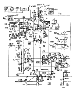
A horizontal deflection circuit 250 of FIGURE 2,
embodying an aspect of the invention, provides~horizontal
deflection in, for example, an FS color cathode ray tube
(CRT) t~pe A66EASOOXOl. Circuit 250 includes a switching
transistor Ql operating at a horizo~tal freguency f~ and an
anti-parallel damper diode DQl, both being constructed as
one integrated circuit. A retrace capacitance C1 is
coupled in parallel with transistor Ql and diode DQl. A
deflection winding ~ is coupled in series with an
S-shaping trace capacitance Cs to ~orm a circuit branch
that is coupled in parallel with each of transistor Q1,
diode DQl and retrace capacitance Cl to form a retrace
resonant circuit 100 during horizontal retrace.
A phase-control stage 101 that includ~s a
horizontal oscillator and a phase detector, not shown in
detail in FIGURES, is responsive to a horizontal
synchronizing signal Hs. Signal Hs is derived from, for
example, a video detector of a television receiver, not
shown in the FIGURES. Stage 101 applies, via a t~ansistor
Q6, a drive voltage lOla to a primary winding T2a of a
driver transformer T2 that is transformer coupled to a
secondary winding T2b of transformer T2. Winding T2b is
coupled via a voltage divider, that includes resistors R1
.
.
- -,
,
-- 132~38
-4- RCA 85,013
and R2, to the base-emitter junction o transistor Ql for
producing a base drive current ib at the horizontal
frequency fH. A primary winding W1 of a flyback
transformer Tl is coupled between a source of a B+ voltage
and the collector of transistor Q1. ~ secondary winding W2
of transformer T1 is coupled to stage 101 to provide a
feedback retrace si~nal Hr for generating drive voltage
lOla that synchronizes a horizontal deflection current i2
in winding ~ to signal Hs.
A switched raster correction circuit 200,
embodying a feature of the invention, includes an E-W
control circuit 300 that controls the switching timing of a
switching transistor Q2. Transistor Q2 i~ conductive
throughout the trace interval and becomes nonconductive
during a controllable instant within the retrace interval.
The collector of transistor Q2 is coupled to a junction
terminal 50 between the emitter of transistor Q1 and
retrace capacitor C1. The emitter of transistor Q2 is
coupled to ground via a small curre~t sampling resistor
R101. A damper diode DQ2 ,coupled in parallel with
transistor Q2, is constructed with transistor Q2 as one
integrated circuit. A second retrace capacitor C2 is
coupled between the collector of transistor Q2 and the
ground conductor. A retrace voltage Vr generated across a
winding W4 of transformer Tl provides a high voltage, used
for generating an ultor voltage in an ultor power supply
556 that includes rectifying diodes~ not shown in the
FIGURES.
A first hypothetical example that is used for
explanation purpose represents a first extreme operating
condition in which transistor Q2 is maintained conductive
throughout trace and retrace. In this case, deflection
circuit 250 generates deflection current i2 in a manner
that is well known but without East West correction. As
e~plained later on, current i2 is at a ma~imum peak~to-peak
amplitude, in this ca~e.
A second hypothetical example that is also used
for explanation purposes, represents a second extreme
,:
:
,
,..." .
'' ', ~' . : : ,
~ ~32~3~
-5- RCA 85,013
operating condition in which switching transistor Q2 is in
cutoff throughout an entire retrace interval. In the second
example, during retrace, a pair of resonant circuits are
formed. The first one, retrace resonant circuit 100 of
S FIGURE 2, includes retrace capacitor C1, winding ~ and
trace capacitor Cs. The second resonant circuit includes
flyback transformer winding W1 and retrace capacitor C2
that are coupled in series~ Considered ~eparately, each of
the pair of retrace resonant circuits is tuned to a
frequency that is lower than a required nominal retrace
frequency. The resonant circuits are coupled to form a
combined resonant circuit. Therefore, the resulting common
retrace frequency of the combined resonant circuit is
higher than each of its constituents and is made equal to
the required nominal retrace frequency that is,
illustratively, 43 KHz in the PAL system.
As explained before, secondary winding W2 of
transformer Tl provides horiæontal synchronizing retrace
signal Hr. Each pulse of signal Hr represents the retrace
interval in deflection winding ~. Horizontal
synchronizing signal Hr is coupled to phase-control-stage
101 for providing feedback synchronization information.
The synchronization information contained in the pulses of
signal ~r is indicative of the phase of current i2 in
deflection winding LH. Signal Hr and horizontal sync
pulses Hs are used to adju~t the phase and the frequency of
the horizontal oscillator output signal that is included in
stage 101.
In the second hypothetical example, primary
winding Wl of transformer Tl is coupled to retrace resonant
circuit 100 through a capacitiv~ voltage divider that
includes capacitors C1 and C2 to form the combined resonant
circuit. The combined retrace resonant circuit enables
proper synchronization without causing mouseteeth
distortion. The advantages of forming such combined
retrace resonant circuit are explained in detail in U.S.
Patent 4,634,937 in the name of P.E. Haferl, entitled
"EAST-WEST CORRECTION CIRCUIT".
,~
,
. .
- .
-6- 1 32 ~ ~38 RCA 85,013
During trace, current il in winding W1 flows
through transistor Ql and through transistor Q2 to ground.
During retrace, current i1 that flows through capacitor Cl
also flows through capacitor C2 as retrace current i4 and
causes a retrace voltage v2 to be develo~ed across retrace
capacitor C2.
The amplitude of a retrace voltage V1, developed
across the series coupled CapacitQr C1 and C2 is stabilized ~--
by the B+ voltage that is regulated. Therefore, voltage V
is, ad~antageously, substantially unaffected by th
East-West modulation. Retrace voltage V4, developed across
winding LH and across capacitor C1, determines the
amplitude of deflection current i2. Retrace voltage V4 is
equal to retrace voltage Vl minus retrace voltage V2.
Because current i3 in transistor Q2 is zero during the
second portion of retrace when transistor Q2 is
nonconductive, retrace current il flows substantially
entirely as current i4 through capacitor C2 and generates
retrace voltage V2. It follows that in the second
hypothetical example in which transistor Q2 is
nonconductive throughout retrace, voltage V2 is at a
maximum amplitude. Consequently, voltage V4 amplitude is
at a minimum and deflection current i2 is also at a minimum
in the second hypothetical example.
Modulation of deflection current is obtained by a
modulation of the turn-off instant of transistor Q2 during
the first half of the retrace interval in a way that
mouseteeth distortions are reduced. By selecting the
value of capacitor C1 to be, for example, approximately
twice that of capacitor C2, and the value of the inductance
of winding W1 to be approximately twice that of winding ~,
the retrace frequency remains the same during both the
first portion of retrace, when transistor Q2 is conductive,
and during the second portion Qf retrace, when transistor
Q2 is nonconductive. Consequently, the phase of voltage V
in winding Wl relative to that of deflection current i2 is
unaffected by the conduction state of transistor Q2.
Modulation of the turn-off instant is permissible because
"
.,: .
--` 1 32~38
-7- RCA 85,013
both the retrace time and a retrace voltage Vr developed
from voltage vl in winding W4 of transformer Tl are,
advantageously, substantially unaffected by the state of
conductance of transistor Q2, during retrace.
FIGURES la-lh illustrate idealized wavPforms
useful for explaining the operation of the circuit of
FIGURE 2. Similar symbols and numerals in FIGURES 2 and in
FIGURES la-lh indicate similar items or functions.
E-W control circuit 300 of FIGU~E 2 generates a
pulsed voltage V3 which drives the base of transiitor Q2.
Voltage V3 causes transistor Q2 to be conductive throughout
the trace interval. During retxace, the falling edge of
voltage V3 is phase modulated in the range t2-t3 of FIGURE
la. Thus, switching transistor Q2 of FIGURE 2 is
conductive prior to time t2 of FIGURE la and switched into
cut-off after time t2 at the phase modulated instant within
the range t2-t3. When conductive, transistor Q2 clamps
retrace voltage V2 to zero and varies the instant when the
generation of voltage v2 occurs.
Current il in winding W1 of transformer Tl of
FIGURE 2 flows into resonant circuit 100 that includes
winding ~ and capacitor C1. From resonant circuit 100,
current il splits and fonms current i3 and current i4 when
transistor Q2 of FI~UR~ 2 is nonconductive. When
25 transistor Q2 is turned-off, the decreasing current i4 of
FIGURE ld charges capacitor C2 of FIGURE 2 until time t4 of
FIGURE ld, occuring at the center of the retrace interval
when currents i1 and i4 become zero~ As a result, voltage
V2 of FIGURE le reaches its peak amplitude at the center
30 of retrace. During the second half of retrace, negative
current i4 o FIGURE ld, that becomes incre2sing~y more
negative, discharges capacitor C2 of FIGURE 2 until voltage
V2 becomes negative. When voltage V2 becomes sufficiently
negative, diode DQ2 starts conducting and clamps voltage V2 0
35 to -0.6 voltage, the forward voltage of diode DQ2.
The correction of outside pincushion distortion
requires a higher amplitude of deflection current i2 when
scanniny lines ~t the center of the raster than at the top
,, ~ .
..
, : . . . .
~ 32~38
-8- RCA 85,013
or bottom. At the top of the raster, transistor Q2 is
turned off at time t2 of FIGURE la, that is the earliest.
Voltage V2 of FI~URE le starts to increas~ after time t2.
After the center of retrace occurs, voltage V2 decreases
until it becomes zero at time t~. Because transistor Q2 is
turned off at the time t2 at the top of the raster, the
peak amplitude of voltage V2 is at a maximum; consequently,
the peak amplitude of voltage V4 of FIGURE lh is at a
minimum. From the top toward the center of the raster,
the turn-off time of transistor Q2, determined by the
falling edge of voltage V3 of FIGURE la, is increasingly
delayed within interval t2 ~ t3. The result is a
decreasing pea~ amplitude of voltage V2 of FI~URE 2, an
increasing peak amplitude of voltage V4 and an increasing
peak amplitude of deflection current i2. At the center of
the raster, voltage V2 starts increasing at time t3 of
FIGURE le and becomes zero at time t5 of each horizontal
period. From the center toward the bottom of the raster,
the turn-off time of transistor Q2 of FIGURE 2 is
increasingly advanced from time t3 to time t2 of FIGURE la,
resulting in an increasing voltage V2 of FIGURE 2, a
decreasing voltage V4 and a decreasing deflection current
i2. Thus, deflection current i2 is proportional to retrace
voltage V4 and inversely proportional to retrace voltage V2
that is modulated in accordance with the turn-off instant
of transistor Q2.
The falling edge of voltage V3 of FIGURE la is
phase modulated in a par~bolic manner at a vertical rate to
obtain the vertical rate envelopes shown in conjunction
with waveforms le, lf and lh. Advantageously, the
variation of the turn off time of transistor Q2 of FIGURE 2
modulates also the time when voltage V2 of FIGURE le
becomes zero near the end of retrace.
The center of the retrace pulse waveform of
voltage V2 during horizontal retrace is maintained the same
relative to the center of horizontal retrace time t4
throughout vertical scan. Thus, voltages V4 and V2 of
FIGURE 2 are maintained in phase with respect to voltage
: ,~
, ~
.: ,
9 1326~38 RCA 85,V13
Vl. It follows that, advantageously, signal Hr is maintained in
phase with deflection current i2.
Signal Hr developed across winding W2 provides phase
information of the phase of deflection current i2. Signal Hr is
5 applied to stage 101 for synchronizing the horizontal oscillator of
stage 101 to sync pulses Hs of the video signal. Because capacitor
C2 couples winding W1 to winding LH to form a combined
resonant circuit, the phase information of signal Hr is substantially
identiGal to that of deflection current i2. Further advantage is
10 provided by the switched operation of transistor Q2 is that
inductive components are not required to be coupled in series
with transistor Q2. Also, the switched operation of transistor Q2
results in low power dissipation in transistor Q2. Therefore,
transistor Q2 may not require a heat sink. An additional
15 advantage over other east-west circuits such as a conventional
diode modulator is that deflection current i2 does not flow through
a damper diode during the second half of trace, resulting in lower
deflection losses and lower asymmetric linearity error.
As explained before, during retrace, deflection
2 0 resonant circuit 100 is coupled to flyback transformer T1 by
capacitor C2 having a high impedance, after transistor Q2 becomes
nonconductive. When transistor Q2 becomes nonconductive, the
ultor voltage rectifying diodes, not shown, are conducting. The
high impedance of capacitor C2 substantially isolates windings LH
2 5 and Wl at frequencies associated with mouseteeth distortion that
are substantially lower than the retrace frequency of resonant
circuit 100 during retrace; thereby, raster distortions known as
mouseteeth are prevented from occurring. The manner by which
mouseteeth are prevented is further explained in Canadian Patent
3 0 Application 593,225, filed 9 March 1989, i~i the name of the same
Applicant, entitled, RASTE~R DISTORTION CORRECTED DEFLECTION ,~
CIRCUIT.
Junction terminal 50, between capacitors C1 and C2, is
clamped to ground potential by transistor Q2 during the entire
3 5 trace interval. Therefore, raster disturbances
~: .
.
.
. . .
lo- ~326~38 RCA 85,013
referred to as "Organ Pipes" do not appear. Organ Pipes
type raster disturbances may occur if such clamping were
not used, as a result of oscillatory current or ringlngs in
the flyback transformer primary current. Such ringlngs are
suppressed because transistor Q1 is clamped to ground by
transistor Q2 during the entire trace interval.
Advantageously, damper diodes DQl and DQ2 may be
constructed with the corresponding transistor using the
integrated circuit technology for further reduci~g the
required discrete components count.
E-W control circuit 300 of FIGURE 2 includes a
differential amplifier formed by transistors Q3 and Q4 and
Darlington driver transistor Q5 which drives switching
transistor Q2. The differential amplifier that includes
transistors Q3 and Q4 compares a vertical parabola voltage
V6 to an exponentially shaped ramp portion V5a of a voltage
V5 having a waveform that is shown in FIGURE 2~. The
crossover points of the compared voltages determines the
timing of control voltage V3 of FIGURE la.
To develop voltage V5 of FIGURE 2, horizontal
retrace pulses ~3 of FIGURE 2, developed in a winding W3
of transformex T1, are coupled via a resistor R4 to a zener
diode D3. A speed-up network that includes a capacitor C4,
a resistor R5 and a diode D2 generates a gating pulse VD3
across diode D3 having a leading edge with a fast rise
time. Faster leading edge results, advantageously, in a
larger d~namic range of E-W control circuit 300. Pulse VD3
across diode D3 is applied via resistors R6 and. R7 to a
capacitor C5 and to a resistor R9 for generating the
3Q exponentially shaped ramp portion VSa of voltage V5.
Pulsed voltage V5, that includes exponentially increasing
top portion V5al is applied to the base of transistor Q4. A
vertical rate parabolic voltage Vp of FIGURE 2 that
includes a superimposed sawtooth voltage is coupled from a
DC blocking capacitor Cc of a conventional vertical
deflection circuit 350 to the base Qf transistor Q3 via a
capacitor C8, a resistor R20 and a resistor R14. Resistors
R14, R15 and R16 provide dc bias to the base of transistor
" ... . . . . ~
~ 132~3~ RCA 85,013
Q3. Voltage V2, that is coupled via a resistor R13 to the
base of transistor Q3 and to an integrating capacitor C6,
pxovides a negative feedback, causing the vertical ratP
envelope o voltage V2 to track parabolic voltage Vp that
is developed in capacitor Cc.
A v~rtical sawtooth voltage VRs developed across
a sampling resistor Rs is coupled, via a resistor ~10 and a
resistor R9, to a capacitor C5 for developing a voltage V7
having an exponential upramping portion at a peak amplitude
that is determined by voltage VRs. Voltage V7 is coupled
to the base of transistor Q4 of control circuit 300. In
this way, Voltage VRs is also coupled via capacitor Cc to
the base of transistor Q3. Because voltage VRs is applied
in a diffexential manner, voltage VRs is prevented from
substantially affecting the switching operation of
transistors Q3 and Q4. A vertical parabola voltage V6
developed at the base of transistor Q3 is compared to
horizontal ramp voltage VS. The crossover points of
voltages V5 and V6 determine the timing of the leading and
trailing edges of voltage V3, as indicated before.
E~ponentially shaped ramp portion V5a of voltage
V5 linearizes the east-west modulator circuit 200 by
compensating for the decreasing level of current il of
FIGURE lb, during retrace. Linearization oc~urs because a
small amount of modulation of voltage V3 near time t~ of
FIGURE la results in a higher amplitude modulation of
voltage V2 of FIGURE le than the same amount of modulation
of voltage V3 near time t3 of FIGURE la. This is so
because the amplitude of each of currents i1 and i4 of
FIG~RES lb and ld, respectively, is higher at time t2 than
at time t3 and because voltage V2 is proportional to the
value of fi4. dt. The exponentially shaped ramp voltage V5
is steeper near time t2 than at time t3 of FIGU~E lg.
Conseguently, for a given voltage vari~tion at ~he base of
transistor Q3, the the modulation of voltage V3 is smaller
around time t2 than around time t3. Thus the exponentially
shaped ramp portion V5~ of voltage V5 linearizes the
operation of E-W raster correction circuit 200.. Resiætor
.
' ~
12- 132~538 RCA 85,013
R15 raises the dc average of voltage V5. Compensat1on of
picture width variations as a function of beam current,
tha~ may be referred to as anti-breathing, may be applied
via the basP of transistor Q3.
Transistor Q5 of FIGURE 2, ha~ing a base that is
coupled to the junction of a load resistor R12 and a
collector of transistor Q3, applies a base drive ko
transistor Q2 from a load resistor R17 that is coupled to
the collector of transistor Q5. The collector of
transistor Q5 is coupled via a parallel arrangement of a
capacitor C7 a~d a resistor ~18 for generating a fast
transition of a falling edge portion of voltage V3 to
obtain a ~ast turn-off of transistor Q2. The fast turn-off
allows interrupting current i3 immediately after time tl of
FIGURE lc and allows using the full modulation range
between time tl and t4. Illustratively, the turn-off delay
of transistor Q2 of FIGURE 2 is less than 1 microsecond.
The use of a MOSFET in place of Q2 may fuxther reduce the
turn-off delay. The fast turn-off feature may be desirable
in a situation that requires a deflection current at, ~or
exa~ple, a higher frequency such as 2xfH.
A protection diode Dl, embodying a feature
of the invention, is coupled between the collector of
transistor Q2 and a terminal Wla of primary winding W1 of
transformer Tl. ~iode Dl protects transistor Q2 from
e~cessive peak voltage that may occur when power is
initially turned on. Transistor Q2 is protected by diode
Dl which limits voltage V2 to a maximum of 350V.
Transformer T2 has, preferably, 400V isolation capability
between the primary and secondary windings.
A remote control receiver 201 generates an on/off
control signal 2Qla that is coupled to an on/off transistor
switch Q7 of a +12V regulator. When transistor Q7 is
nonconductive, an output supply voltage +l~V is generated
that causes phase-control-stage 101 to be energized during
power-up. When transistor Q7 is conductive, stage 101 is
de-energized that causes stand-by mode operation. During a
transition to the stand-by mode, phase~control-stage 101,
., :.
,
13- 1326~38 RCA 85,013
that supplies base drive to the base of transistor Q6,
causes driver transistor Q6 of transformer T2 to be
turned-off.
After, for example, the transition from normal
operation to the stand-by mode operation, there may still
be energy stored in primary winding T2a of transformer T2
of FIGURE 2. This energy may continue producing base
current ib in deflection transistor Q1 until a mag~itude of
voltage lOla across primary winding T2a of transformer T2
decreases to zero. As a result, a final deflection cycle
may be generated with an extended but undefined time
duration that ends when transistor Ql ceases to conduct.
- Consequently, currents il, i2 and i3 might increase
e~cessively and destroy transistors Q1 and Q2.
In accordance with another feature of the
invention, to prevent such a possibility, on/off control
signal 201a is coupled through a resistor R81 ~nd a
conductor 555 to the base electrode of a transistor Q5 that
provides base drive to transistor Q2, causing transistor Q2
to turn off immediately after the power-on-to-standby
transition. Since both transistors Ql and Q2 a~e coupled
in series, turning off transistor Q2 causes the current in
both transistors to cease. Thus transistors Ql and Q2 are
protected. However, such fast shut-down arrangeme~t may
25 require a fast spot suppression circuit to prevent a beam ~.
spot related damage to the CRT, not shown.
In an alternative protection arrangement,
embodying a fur~her feature of the invention, in which the
aforementioned fast spot suppression circuit,
advantageously, may not be required is also shown in FIGURE
2. In such preferred arra~gement, a feedback arrangement
that includes a series arrangement of a diode D10 and a
resistor R91 is coupled between the emitter of transistor
Q2, as shown by the dashed line, and the base of transistor
Q5, via conductor 555. When such feedback arrangement is
used, the emitter of transistor Q2 is coupled to ground via .
current sampling resistor R101 causing current i3 to be
sampled across resistor R101. A resulting voltage VOC
.
i~" 14 132~538 RCA 85,013
developed across resistor R101 controls the base voltage of
transistor Q5. When voltage VO~ across resistor R101
e~ceeds -~1.8V, transistor Q5 is turned on by voltage VOC
and reduces the base drive of transistor Q2. Thus, current
i3 is limited to a peak of 1.8 ampere when, for example,
resistor R101 equals 1 ohm.
The feedback provided by diode D10 and resi~tor
R91, advantageously, protects botA transistors Q1 and Q2
that are coupled in series during operation and, in
particular, during the power-up-to-standby transition. It
should be understood that such ~eedback arrangement may
also be used together with, or instead of the arrangement
in which signal 201a is coupled to the base of transistor
Q5 that was explained before. When, for example, both
arrangements are used together, current i3 may become
substantially reduced to, for example, zero for providing
the required protection over-current or for providing
on/off operation.
FIGURE 3a illustrates an envelope of a waveform
of current i3 of FIGURE 2 immediately after corresponding
transitions between normal operation power-up mode and
standby mode without the protection circuit, that would
occur if conductor 555 were disconnected for disabliny the
operation of the protection circuit. Similarly, FIGURE 3b
illustrates the envelope of the waveform of current i3 of
FIGURE 2 when conductor 555 is connected that enables the
operation of the protection circuit. Note that current i3
of FI~URE 3b is limited to the maximum of 1.8 amperes.
Likewise, FIGURE 3c illustrates an envelope of the collector
current of Ql of FIGURE 2 when the protection circuit is
disabled and FIGURE 3d illustrates the envelope of collector
current of Ql of FIGURE 2 when the protection circuit is
enabled.
. ~ ~