Note: Descriptions are shown in the official language in which they were submitted.
1 326892
BACKGROUND OF THE INVENTION
This invention relates to an optical ~witch for
conducting and interrupting an optical path and an optical
keyboard which utilizes the optical switch.
A measuring controller, a machine controller, and a
monitor controller, etc. have mostly employed in general as
signal control means an electric system signal devices.
Such electric system signal device~ have been
feasibly affected by electromagnetic induction near a power
plant, a substation or a power transmission line as has been
pointed out, and a spark generated from an electric contact
sometimes causes a fire in environments where combustible gas
exists.
To eliminate such defects; mean~ for remotely
controll$ng these devices have been provided, but in case of
remote control, the suitability and the rapidity of the
signal control are defective.
Further, in the case of electric system signal
devices, corrosion resistance 18 also defective due to the
generation of static electricity at the slgnal input unit and
the electric contacts made of metal conductors.
To obviate such drawbacks it is desirable to
construct a predetermined optical signal control system
mainly with optical switches, and the optical signal control
system can almost solve the above-mentioned drawbacks.
A general example of the optical switch applied to
the optical signal control signal di8closed in Japanese
Utility Model Publication No. 14014/1986 conducts and
interrupts an optical path by attaching rod lenses to the
ends of a pair of optical fibers for forming the optical path
80 that the ends are opposed in a housing and a light
shielding plate is telescoped in or out between the rod
lenses.
In the known example, since expensive components,
such as the rod lenses have been employed, the optical
- 2 - ~n-
C
. .
' "' 1 3268q2
switches become expensive.
In order only to reduce the cost, an optical switch
in which the end faces of the optical fibers are directly
opposed without rod len~es can be considered.
For example, optical fibers having large diameter of
cores are selectively used, and the coupling loss of the
optical fibers in a light passing state can be reduced by
decreasing an interval between the end faces of the optical
fibers.
However, if the interval between the end faces of the
optical fibers is reduced, a light shielding plate telescoped
in or out of the interval must be reduced in thickness.
Thus, if the interval between the end faces of the optical
fibers and the light shielding plate is not accurately formed
correspondingly, the end faces of the fiber~ are damaged due
to the contact of the end faces of the optical flbers and the
light shielding plate to cause a foreign material to be
bonded thereto 80 that the manufacture of the optical fiber
becomes difflcult.
Particularly, the damage and the adherence of a
forelgn material to the end faces of the optical fibers have
become large problems in plastic optical fibers.
When the interval between the end faces of the
optical fibers i8 reduced and the thickness of the light
shielding plate i8 reduced in order to reduce the coupling
1088 between the optical fibers or to simplify the optical
~witch, an optical signal is passed through the thin light
~hielding plate with the result that the interruption of the
optical path is incomplete.
In other devices, the optical switch must be made as
small as possible to be associated therein, and it i8 very
important that the assembling structure is stable and the
attachment to a keyboard is facilitated.
SUMMARY OF THE INVENTIO_
~ccording to one aspect of the invention there is
provided an optical switch, comprising: a pair of large
C - 3 -
:
,
. ,
. 1 326892
diameter optical fibers; a housing having an opening at each
end thereof; sleeves into which the ends of the fibers are
inserted, each sleeve being fitted into one opening of the
housing, the sleeves so fitted being positioned on the same
longitudinal axis; a stopper on the inner surface of the
housing, the stopper projecting inwardly to form an abutment
for each sleeve and thereby provide a predetermined space
between each sleeve and fiber end face; and a light
shielding plate moveable into or out of the space between the
end faces of the optical fibers in the sleeves for
selectively interrupting or permitting optical continuity
between the fibers in each sleeve.
According to another aspect of this invention, there
is also provided an optical keyboard formed of optical
switches, each switch including a pair of large diameter
optical fiber~; ~leeves into which the fibers are inserted;
a housing in which the fiber-containing sleeves are retained,
the sleeves being in longitudinal alignment with each other;
a stopper on the inner surface of the housing, the stopper
establlshing a predetermined distance between the end faces
formed at the end of the each sleeve and the fiber therein;
and a light shielding plate disposed telescopically between
the end faces for effecting or interrupting an optical path
between the optical fibers, both the optical fibers and the
light shi~lding plate being displaced to one side in the
housing, whereby the optical switches are attached to a
switch mounting board to form an optical switch row, the
fibers in each switch row being substantially longitudinally
aligned.
The above and other related features of the invention
will become apparent from the following description and
accompanying drawings.
BRIEF DESCRIPTION OF THE DRAWINGS
Figs. 1, 2 and 3 are partly cutout.front, side and
plan views showing an embodiment of an optical switch
according to the present invention;
C - 4 -
.
1 ~26892
Fig. 4 is a horizontal sectional view showing the
vicinity of a sleeve in the optical switch;
~ ig. 5 is an enlarged horizontal sectional view
showing the vicinity of a light shielding piece of the
optical switch;
Fig. 6 is a plan view of a substrate on which the
optical switch is mounted;
Fig. 7 is a perspective view of the optical switch
mounted on the substrate;
Figs. 8 and 9 are sectional views showing the
essential portions of various examples of means for fixing
the sleeve in the housing of the optical switch;
Fig. 10 i8 a perspective view of a stopper used for
the fixing means of Fig. 8;
Fig. 11 is a plan view schematically showing one
embodiment of an optical keyboard utilizing the optical
switch according to the present invention; and
Fig. 12 is an explanatory vlew schematically showing
the example of uslng the optical keyboard.
DESCRIPTION OF THE PREFERRED EMBODIMENTS
Embodiments of an optical swltch and an optical
keyboard utilizing the optical switch according to the
present invention will be described in detail with reference
to the accompanying drawings.
The optical switch of this invention will be first
described.
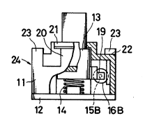
An optical switch 24 shown in Figs 1 to 5 comprises
a plastic housing body 11, a bottom plate 12 of the housing,
an elevationally movable operation shaft 13 driven under the
guidance of the inner surface of the housing body 11, and a
compre~slon spring 14 interposed between the operation shaft
13 and the bottom 12.
Reference numerals 15A and 15B designate a pair of
optical fibers, and numerals 16A and 16B denote sleeves
fixedly secured to the outer peripheries of the ends of the
optical fibers 15A and 15B, respectively.
-- 5 --
C
~`` 1 326892
Each of the sleeves 16A and 16B has an opening formed
at the center. The optical fibers 15A and 158 are
respectively inserted into the openings of the sleeves 16A
and 16B to be bonded to and integrated with the ends of the
optical fi~ers 15A and 15B.
The optical fiber 15A and the sleeve 16A, and the
optical fiber 15B and the sleeve 16B are polished at their
respective end faces in the integrated state so that the end
faces become coplanar.
Sleeve guide openings 17A and 17B are horizontally
formed in the housing body 11 to be disposed at the side of
the operation shaft 13, and the sleeves 16A and 16B
respectively integrated with the optical fibers 15A and 15B,
and are respectively inserted into the guide openings 17A and
17B to be aligned on the same axis.
A stopper 18 projecting upwards from the inner
surface of the housing is formed between the guide openings
17A and 17B on the inner surface of the housing body 11.
The stopper 18 pro~ects in contact with the ends of
the sleeve~ 16A and 16B and has a helght such that the ends
of the optical fibers 15A and 15B do not contact because of
the stopper 18.
Thus, the ends of the sleeves 16A and 16B inserted
into the guide openings 17A and 17B contact both side
surfaces of the stopper 18 so that the interval between the
end faces of the optical fibers 15A and 15B is maintained
constant.
The sleeves 16A and 16B are bonded iixedly to the
housing body 11 in this ~tate.
A light shielding piece 19 80 integrally projects as
to be introduced between the end faces of the optical fibers
15A and 15B.
As shown in Fig. 5, the light shielding piece 19 has
a thick portion l9a having a thickness to be inserted into
the gap between the end faces of the sleeves 16A and 16B at
the base end side of the light shielding piece 19, and a thin
C ~ - 6 -
.
. .
: ~ ' ' ~ '' ';
- 1 326892
portion l9b reduced in thickness from both sides toward the
end side.
It is noted that the alternative shape of such a
light shielding piece 19 has a tapered shape that the
thickness is gradually reduced from the base end side toward
the end side.
When the operation shaft 13 is moved upward or
downward, the light shieldiny piece 19 is fed at the thin
portion l9b between the end faces of the optical fibers 15A
and 15B, and is fed at the thick portion l9a between the end
faces of the sleeves 16A and 16B without passing between the
end faces of the optical fibers 15A and 15B.
Therefore, as shown in Fig. 1, when the thin portion
l9b of the light shielding plate is disposed between the end
lS faces of the optical ~ibers 15A and 15B, an optical path i8
formed.
When the operation shaft 13 is pressed in this state,
the light shielding plate 19 is moved down, and the thin
portion l9b of the light shielding piece 19 is fed through
between the end faces of the optical fibers l5A and 15B,
thereby conducting the optical path.
The thick portion l9b of the light shielding piece 19
is formed upwardly longer than the thin portion l9b 80 that
the thick portion l9a may not be fed out from between the end
faces of the sleeves 16A and 16B even in this state described
above.
When the operation shaft 13 is released, the
operation shaft 13 is returned to the initial position by
means of the recoiling force of the compression spring 14,
and the light shielding piece 19 interrupts the optical path.
Thus, the optical path is conducted and interrupted.
The reason why the thick portion l9a and the thin
portion l9b are formed on the light shielding piece 19
described above is because the light shielding piece 19 does
not contact the end faces of the optical fibers 15A and 15B.
In a concrete example, the optical switch in which
: ~ - 7 -
.
,
1 ~26892
plastic optical fibers 15A and 15B having 0.5 mm of diameter
were opposed at an interval of 0.38 mm at the end faces
thereof, the thickness of the thick portion l9a of the light
shielding piece 19 was 0.35 mm, and the thickness of the thin
portion of the light shielding piece 19 was 0.26 mm, as
determined by trial.
With the optical switch 24 of this example the
coupling loss of the light passing state was 1.4 to 1.8dB.
The assembly of the optical switch 24 will now be
described.
Elastic tongue pieces 20 each having an outward
engaging pawl 21 are respectively formed at the upper left
and right sides of the housing body 11, lower contacting
surfaces 22 lower than the lower surfaces of the engaging
pawl 21 are respectively formed at the upper front and rear
sides of the housing, and positioning projections 23 are
respectively formed at upper four corners of the housing body
11 .
A stepwi~e differance T from the lower surface of the
engaging pawl 21 to the contacting surface 22 corresponds to
the thickness of a substrate 25 to be descrlbed later.
As is apparent from Figs. 6 and 7, an opening 26 i~
formed at a substrate 25 on which the optical switch 24 is
mounted.
25In Fig. 7, when the optical ~witch 24 having the
optical fibers 15A and 15B iQ intruded from the lower side of
the substrate 25 into the opening 26, the engaging pawl 21
initially sliding on the inner surface of the opening 25 is
moved to the inside, the elastic tongue piece 20 is then
deflected, and the contacting surface 22 is then contacted
with the lower surface of the substrate 25. At this time,
the engaging pawl 21 is relatively engaged with the upper
edge of the opening 25 by the recoiling strength of the
elastic tongue piece 20.
35Thus, the substrate 25 is held between the lower
surface of the engaging pawl 21 and the contacting surface
- 8 -
, ~\ , .
.
.
"~ :
- ~ ' ` ' .
1 326892
22, and the optical switch 24 is fixed to the substrate 25
without displacing.
Further embodiments of an optical switch 24 according
to this invention will now be described.
In the embodiment described above, the optical switch
14 in which the optical path conducts when the operation
shaft 13 i8 pressed and is interrupted when the operation
shaft 13 is released, is provided. However, the optical
switch 24 may also be turned ON and OFF by the re~erse
operations to the above, and the conducting and interrupting
states may also be held within the scope o~ this invention b~
slightly modifying in design or an additional structure.
The light shielding piece 19 may al~o have a
predetermined thicknes~ without the thick portion l9a and the
thin portion l9b.
At least ~he thin portion l9b of the light shielding
piece 19 is made of an opaque material having a light
shielding function as known per se, and when the thin portion
l9b is particularly thinly formed, a light absorbing materlal
may be contained in a part (in the thin portion l9b) or the
entirety oi the light shielding plate 19 so as to reliably
shield the light at light shielding time, i.e., to prevent
the light from passing therethrough.
For example, when the light shielding piece 19 is
formed of plastic, such as ABS, or polycarbonate, the plastic
light shielding piece 19 contains, for example, the li~ht
absorbing material made of carbon.
In a concrete example, when the thickness of the thin
portion l9b of the plastic light shielding piece 19 was
0.3 mm and the carbon content rate of the light shielding
piece 19 was approx. 0.5%, the light permeability attenuation
rate at light interrupting time of the light shielding piece
19 was approx. 25 to 30dB, but when the carbon content rate
was 2~ or higher, the light permeability attenuation rate
was increased by 10% or more.
The carbon content rate of the light shielding piece
_ 9 _
.
,~
1 326892
19 is desirably set to a range so as not to lose the
moldability.
Other members except the optical fibers 15A and 15B
such as the hou~ing body 11, the bottom plate 12 and the
operation shaft 13 are molded of plastic which contains the
light absorbing material as required.
In a concrete example, when the housing body 11 and
the bottom plate 12 are molded of the plastic having approx.
0.5 to 1% of carbon content, it is desirable to mold the
operation shaft 13 including the light shielding piece 19 of
plastic which contains approx. 3 times that carbon content.
When the light shielding piece 19 and the other
members are molded of plastics which have equal light
absorbing material content rates, the light absorbing
material content rate of this ca~e is desirably 2% or more by
weight.
When the ends of the optical fibers 15A and 15B can
be increased, the members except the sleeves may be attached
to the ends of the optical fibers.
As means for flxing the sleeve~ 16A and 16B in the
guide openings 17A and 17B to the housing body 11, means
shown in Figs. 8, 9 and 10 may be optionally employed instead
of the bonding means described above or together with the
bonding means.
In the case of Fig. 8, elastically deformable pawl
pieces 27a and Z7b are integrally formed with the housing
body 11 at the inlet ends of the guide openings 17A and 17B
of the housing body 11.
In Fig. 8, the sleeves 16A and 16B inserted
respectively into the guide openings 17A and 17B are,
similarly as described above, held by the pawl pieces 27a and
27b in the inserted state, and the ends of the sleeves 16A
and 16B are contacted with both the ends of the stopper 18 by
the pressing strengths of the pawl pieces 27a and 27b 80 that
the sleeves 16A and 16B are held at predetermined positions
in the housing body 11.
-- 10 --
' ' '
: . .
1 326892
In the case of Fig. 9, a channel type stopper 28
shown in Fig. 10 is employed.
Such a stopper 28 is formed of a metal or a plastic
spring material, and is composed of retaining pieces 30a and
30b having slits 29a and 29b, and a coupling piece 31 for
coupling the base ends of both the retaining pieces 30a and
30b.
In the stopper 28, the narrowest interval between the
retaining pieces 30a and 30b is shorter than the width of the
housing body 11.
In the case of Fig. 9, after the sleeves 16A and 16B
are respectively in~erted into the guide openings 17A and
17B, the stopper 28 is attached from the bottom side of the
housing body 11 over both sides, and the retaining pieces 30a
and 30b of the stopper 28 are pressed at the rear end faces
of the sleeves 16A and 16B toward the stopper 18. Thus the
end faces of the sleeves 16A and 16B are contacted with both
8ide faces of the stopper 18 through the pre~sing ~trengths
of the retalning pieces 30a and 30b, and the sleeves 16A and
16B are h~ld at predetermined positlons in the housing body
11 .
In this case, the optlcal fibers 15A and l5B are
engaged within the slits 29a and 29b of the retaining pieces
30a and 30b.
The stopper 28 described above may also be attached
from the front sides of the housing body 11 over both sides
thereof, and the directions and the shapes of the retaining
pieces 30a and 30b and the directions of the slits 29a and
29b may be suitably selectively determined in respon~e to the
attaching direction, and the slits 29a and 29b may be omitted
as reguired.
In Fig. 11, an optical keyboard 50 comprises a switch
mounting board 51, and a number of optical switches 24
mounted on the ~witch mounting board 51.
In the case of the optical switches 24 as described
above, the optical fibers 15A and 15B and the light shielding
- C 3 - ll -
.. , , . : ~ , ', .
1 3268q2
piece 19 are displaced to one side in the housing 11.
In the optical keyboard 50, the optical switches 24
are mounted, for example, on the switch mounting board 51
sim$1arly to the mounting procedure to the above-mentioned
substrate 25, predetermined number of optical switches 24
are arranged in I, I I and III rows.
The optical switches 24 of the I, II and III rows
mounted on the switch mounting board 51 are aligned
substantially on one line of the leads 15A and 15B of the
10optical fibers 15A and 15B at both sides of the housing 11.
Thus, optical fibers 53A and 53B led from an optical
cable 52 are respectively connected to the optical fibers 15A
and 15B of the optical switch 24 mounted on the switch
mounting board 51.
15Since the optical fiber leads 15A' and 15B' are
aligned on one line in the optical keyboard 50 of Fig. 11,
the optical fibers can be readily wired and corrected 80 that
unreasonable bends are not formed at the optical fibers 15A
and 15B.
20Fig. 12 shows a concrete example of the optical
keyboard 50 using the optical switches.
In the case of Flg. 12, one end of the optical cable
52 is connected to the optical switches 24 of the optical
keyboard 51 as described above, optical fiber arrays 54A and
54B are connected respectively to the optical fibers 53A and
53B at the other end side of the optical cable 52, and light
emitting element array 55A and photodetector array 55B are
respectively connected to the optical fiber arrays 54A and
54B.
30When the optical keyboard 50 constructed as described
above is used in a combustible gas environment, the
photodetector array 55B is preferably separated from the
optical keyboard 50 due to explosionproof remedy, and it i8
also true when the optical cable is distinguished between for
light transmitting and receiving operations.
The optical switch of this invention is 80
- 12 -
~ , ' .
. , , . -: . , . . : . , .
. ~ ;, : .' - ', ' . . ' '. '
. .: .
. . ~ , .
- 1 326892
constructed that the ends of the optical fibers are of large
diameter, the large-diameter ends of the optical fibers are
contacted with both side stoppers in the housing to hold the
interval between the end faces of the optical fibers. Thus,
the optical switches disposed at a constant interval between
the end face~ of the optical fibers can be simply assembled.
When the sleeves are mounted on the outer peripheries
of the ends of the optical fibers and the ends of the optical
fiber~ are formed in large diameters in the optical switch of
this invention, the ends of the optical fibers can be readily
increased in diameter. Further, when the end faces of the
sleeves are contacted with the stopper, the interval between
the end faces of the optical fibers can be set to a
predetermined value without damaging the end faces of the
optical fibers.
When the housing has the optical shaft movable
reciprocally in a direction perpendicular to the axes of both
the optlcal fibers with the housing as a guide and the light
shlelding piece telescoped ln or out between the end faces of
the optlcal fibers corresponding to between the end faces of
the optical fibers i8 mounted on the side of the operation
shaft in this invention, a space necessary to guide the
operatlon ~haft and a space necessary to reclprocate the
operation shaft may be provided in the axial dlrection of the
operation shaft to reduce the axlal size of the operation
shaft.
When the light shielding piece has the thick portion
at the base end side or the thin portion at the end side, or
the light shielding piece has a tapered portion convergent
from the base end to the end side in the optical switch of
this invention, even if the lnterval between the end faces of
the optical fibers is reduced in the directly opposed state,
the light shielding plate is not contacted with the end faces
of the optical fibers to eliminate the damage of the end
faces of the optical fibers.
When the light shielding piece is made of pla~tic
~ 6~ 13
., .,. ... . - , ~ . . -
. - . . .
. .
- 1 326892
having light absorbing property in the optical switch of this
invention, the light shielding property of the light
shielding piece i8 improved, the thin light shielding piece
may reliably interrupt the light, the light coupling loss can
be reduced and the optical switch can be reduced in size by
decreasing the interval between the end faces of the optical
fibers in response to the thin light shielding piece.
When the elastic tongue pieces having outward
engaging pawls at the upper ends thereof are formed at the
upper right and left sides of the contacting surfaces lower
than the lower surfaces of the engaging pawls are formed at
the upper front and rear sides of the housing in the optical
switch of this invention, the optical switch can be mounted
by a simple operation of merely pres~ing the top of the
optical switch to the opening of the substrate, and when
positioning pro~ections are formed at upper four corners of
the housing in this ~itate in the optical switch of thi~
lnvention, the optlcal switch can be mounted more firmly.
Since the optical keyboard of this invention iQ 80
constructed that, in the relative configuration of the
optical switch and the switch mounting board described above,
both the optical fibers and the light shieldlng plate are
displaced to one side in the housing, the plurality of said
optlcal swltches are attached to a switch mounting board to
form an optical switch row, and the optical fiber leads of
the optlcal switches of the optical swltch row are allgned
substantially on the same line, the optical fibers can be
readily wired and connected, and, in this case, unreasonable
bends are not formed at the optical fibers, and suitable
6ignal control can be safely, rapidly and simply performed at
electromagnetic induction generating positions or under
combustible gas environments.