Note: Descriptions are shown in the official language in which they were submitted.
1326901
BACKGROUND OF THE INVENIION
`''';
Field of the lnvention
This invention relates generally to method and apparatus for recording and/or
reproducing digital data on/from slant tracks of a tape recording medium and, more
particularly, is directed to method and apparatus for r~ecording and/or reproducing digital data
with error correction codes.
Description of the Pfior Art
A digital video tape recorder (Vl~), in which a video signal is recorded on and
reproduced from slant tracks of a magnetic tape by a digital video tape recorder (V~I~), is
proposed and one of recording formats of the digital Vl~ is disclosed in Japanese laid open
patent publication No. 40573/85. In such the digital VTR, each field of television signal is
analog to digital converted and the digital data is recorded on consecutive four slant tracks
of the magnetic tape.
First redundancy symbols each of eight bits for an outer error correction code are
generated from a first predetermined number of symbols each of eight bits and constitute an
outer error correction block together with the first predetermined number of symbols.
Second redundancy symbols each of eight bits for an inner error correction code are
generated from a second predetermined number of symbols which are taken from the shuffled
symbols in the outer error correction code blocks and constitute an inner error correction
block together with the second predetermined number of symbols.
.~
.:~
. ,' t~lL
- 2 -
.,.
.
,.~
,
, ~3
:~, ..
": :1: . . .. ., ,, ,.; ~ ; . . . .
~. . . ~: .: ............. . .
1326901
In the beginning portion of the slant track where the reproducing head starts tracing
the track, the reproducing signals are not obtained sufficiently so that digital data is not
` extracted appropriately. Therefore, the reproduced data may contain many errors.
Specifically, in special reproducing modes such as operation with track jumping by a
dynamic tracking head, the reproducing head traces the tracks every several tracks
intermittently, so that relatively long burst error occurs in the reproduced data, length of
which exceeds the error correction ability of the inner code and outer code. Eventually, such
errors remain uncorrected.
"''
~ OBJECTS AND SUMMARY OF THE INVENI~ON
..
Accordingly, it is an ob~t ~f this invention to provide an improved method
and apparatus for recording and/or reproducing digital data, and which can avoid the above
~described disadvantages of the prior art.
,~,
More specifically, it is an object of this invention to provide method and
apparatus for recording and/or reproducing digital data, which can reduce the number of
erroneous symbols contained in information data even if much erroneous data is included in
the reproduced data.
, ~
According to a first aspect of the present invention, a method for recording
digital data comprises the steps of receiving a series of digital data; dividing said series of
digital data into respective blocks e~ch :ncludillg a first predetermined number of data
symbols; generating outer error correction code block including said first predetermined
number of data symbols and a second predetermined number of redundancy symbols;
i~j generating
,,~j
" .,,
~:;
.~ .
~ -3-
''.'1 ,
",. .~ ~
`,!
, .
. ' , .
.'_`, ' :
: - ' ' .
;'. ' ` . ~ :
:' '
, . .
... . . ' . ' '
\ 132~9~
. .
inner error correction code block including a third predetermined number
of data symbols and a fourth predetermined number of redundancy
symbols; and recording said series of digital data with said redundancy
symbols of said outer error correction code block and inner error
correction code block on slant tracks of a tape recording medium, whereby
said redundancy symbols of said outer error correction code block is
recorded first and followed by said data symbols and said redundancy
symbols of said inner error correction code block on the slant tracks.
According to a second aspect of the present invention, an apparatus
for recording digital data comprises circuit for receiving a series of digi~:al
data; circuit for dividing the series of digital data into respective blocks
each including a first predetermined number of data symbols; circuit for
generating outer error correction code block including the first
predetermined number of data symbols and a second predetermined
number of redundancy symbols; circuit for generating inner error
correction code block including a third predetermined number of data
syrnbols and a fourth predetermined number of redundancy symbols;
circuit for recording the series of digital data with the redundancy symbols
of the outer error correction code block and inner error correction code
block on slant tracks of a tape recording medium, whereby the redundancy
symbols of the outer error correction code block is recorded first and
followed by the data symbols and the redundancy symbols of the inner
error correction code block on the slant tracks.
According to a third aspect of the present invention, a method for
reproducing digital data comprises the steps of reproducing a series of
digital data with redundancy symbols of an outer error correction code
block and an inner error correction
,... .
., i
"-
.".i X
.
".
:,.,
~1
.... .
,
... " , ....... . . . . . .
1326901
code block, whereby said redundancy symbols are generated in such a manner that said series
of digital data is divided into respective blocks each including a first predetermined number
of data symbols, said outer error correction code block is generated so as to include said first
predetermined number of data symbols and a second predetermined number of said
- redundancy symbols and said inner error correction code block is generated so as to include
~ a third predetermined number of data symbols and a fourth predetennined number of said
redundancy symbols and whereby said redundancy symbols of said outer error correction
code block is reproduced first and followed by said data symbols and said redundancy
symbols of said inner error correction code block from slant tracks of a tape recording
medium; decoding said inner error correction code block including said third predetermined
number of data symbols and said fourth predetermined number of redundancy symbols;
tagging an error flag if a predetermined number of error symbols exist in said inner error
correction code block; decoding said outer error correction code block including said first
predetermined number of data symbols and said second predetermined number of redundancy
symbols with said error flag; and outpufflng said series of digital data;
According to a fourth aspect of the present invention, apparatus for
~ reproducing digital data comprises circuit for reproducing a series of digital data with
I redundancy symbols of an outer error correction code block and an inner error correction
~ code block, whereby said redundancy symbols are generated in such a manner that said series
'',5 of digital data is divided into respective blocks each including a first predetermined number
sj of data symbols, said outer error correction code block is generated so as to include said first
1 predetermined number of data symbols
: .
,:s
, i 5
....
.
:'
.
r
.,; ~ . .
.. : ~ ~ . . ... .
... ~ . . .. ; .
.,; ~ . . .. .. .. . - . -
... ~ . . . .. -
.,.,.......... . . .~ ~ .
1~2~9~
and a second predetermined number of said redundancy symbols and said
inner error correction code block is generated so as to include a third
predetermined number of data symbols and a fourth predetermined
number of said redundancy symbols and whereby said redundancy symbols
of said outer error correction code block is reproduced first and followed
by said data symbols and said redundancy symbols of said inner error
correction code block from slant tracks of a tape recording medium; circuit
for decoding said inner error correction code block including said th*d
predetermined number of data symbols and said fourth predetermined
number of redundancy symbols; circuit for tagging an error flag if a
predetermined number of error symbols exist in said inner error correction
code block; circuit for decoding said outer error correction code block
including said first predetermined number of data symbols and said second
predeterrnined number of redundancy syrnbols with said error flag; and
circuit for outputting said series of digital data.
The above, and other objects, features and advantages of $he
invention, will be apparent in the following detailed description of
preferred embodiments, particularly when the same is read in conjunction
with the accompanying drawings in which the same reference numerals are
employed to identify corresponding elements and parts.
,...~
', BRIEF DE~SCRIPIION OF THE DRAWINGS
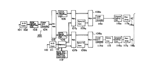
Fig. 1 is a schematic block diagram showing a recording system of a
digital video tape recorder of a type to which the present invention is
desirably applied;
Figs. 2A to 2C are schematic diagrams showing one example
, -6-
, ::
. ~...
.~., ,~, .
. ~
; . .~
;3
'i
.
.,;.
~..
..
- ~, - , . - . . . . . .:
- -,:
. ~, . . : . ~ . .
13269~1
of an inter sector shuffing before o~ter error correction blocks
are formed from a video signal in the inter sector shuffling
circuit in the recording system of Fig. l;
Fig. 3 is a diagrammatic view showing an arrangement of
outer error correction codes from an error correction encoder and
an intra sector shuffing before inner error correction blocks is
formed in the intra sector shuffing circuit each included in the
recording system of Fig. l;
Fig. 4 is a diagrammatic view showing an arrangem~nt of
an inner error correction code from an error correction encoder
also included in the recording system of Fig. l;
Fig. 5 is a diagrammatic view showing a pattern of tracks
in which a video signal and audio signals are digitally recorded
by the recording system of Fig. l;
Fig~ 6 is a schematic block diagram showing a reproducing
system of a digital video tape recorder of a type to which the
present invention is desirably applied;
DETAILED DESCRIPTION OF THE PREFERRED EMBODIMENTS
An apparatus for recording and reproducing digital data
according to the present invention will be hereinafter described
as applied to a video recording system of so-called digital video
tape recorder which is hereinafter simply ref~ered to as a digital
VTR.
;
Referring to Fig. 1, it will be seen that a video
recording system 100 of a digital VTR to which the present
i invention is applied includes a video signal input terminal 101
which receives a composite video signal Sv having 255 lines in
each field in an analog form as shown in Fig. 2A. Such composite
. . .
:
",.,,~s,,,;
. ..................................... ' ' '
. . .
- 1326901
video signal is supplied from the terminal 101 to an
analog-to-digital (A/D) converter 102 in which it is converted,
for example, into 8-bit symbols at a predetermined sampling
frequency, for example, a sampling frequency 4fsc which is four
times color sub-carrier frequency fsc. In the case of a color
television signal according to the NTSC system, 768 effective
samples are provided for each horizontal period or line as shown
in Fig. 2A.
The digitized data from the A-D converter 102 is supplied
to an inter sector shuffing circuit 103 in which the sampled data
for each fiel~ is sequentially divided into three segments in the .-
vertical drection of the field with the result that each segment
contains the data for 85 lines each including 768 pixels, or
65,280 samples as shown in Fig. 2B. Further, the data of each~
segment are scattered over two sectors channel 0 and channel 1 in
such a manner that the sample data is alternately distributed in
the two sectors each including the data for 85 lines each
including 384 pixels, or 32,640 samples as shown in Fig. 2C.
Further, in the inter sector shuffling circuit 103, the data of
the first line in the respective sectors or 384 samples are
distributed in a certain, for example, the first columns (Column
Number 0, 85, 170, 255, 340, 425) of sub-arrays 0 to 5 of a matrix
...
; ~ with an interleaving as shown in Fig. 3 and the data of the second
.l line is in another, for example, the second columns (Column Number
1, 86, 171, 256, 341, 426) of the sub-arrays with a predetermined
. offset starting point a8 shown in Fig. 3.
The data of 32,640 samples in each of the sectors thus
shuffled are 8upplied to an outer error correction code encoder
104 in which the data in each sector are encoded into data with
four parity or redundancy symbols according Reed-Solomon Code at
:, .
~ -8-
.. , . .. ; ~ ,
.. : ~ .,,
: .: ~ ... ~ . . , , :
1326901
every outer code block, which comprised of the data of each column
of the matrix, as shown in Fig. 3. The data of two sectors are
handled in the circuits 103 and 104 so far.
The thus arranged outer-coded data of respective sectors
are provided to a pair of intra sector shuffling circuits 106a and
106b through a de-multiplexer or distributor 105. The intra sector
shuffling circuit 106 has a field memory and a write address
generator and a read address generator, though not shown. The data
of the outer code blocks are supplied to the field memory in the
Column Number 0, 85, 170, 255, 340, 425 and so on, according to
its generating order, under control of the write address generator
so as to be shuffled and ideally arranged in matrix forms each of
~ 64 x 510 samples as shown in Fig. 3.
i The data of 32,640 samples in each of the sectors thusj shuffled are read out from the field memory in the direction ofthe row of the matrix shown in Fig. 3 for generating the inner
~ code blocks under control of the read address generator, whereby
':'...g
i the outer code rows are read out first.
-~ The shuffling process operates identically for all
;~ segments of all video fields. It is assumed that L is the
; television line number within a video segment: L = 0, 1, . . . .
; 84, h is the horizontal sample location within line L: h = 0, 1, .
.'3, ~ ~ 767, and ih is the horizontal sample index following the
channel distribution process or inter sector shuffling mentioned
above: ih 5 integer ~h/2), ih = 0, 1, . . ., 383: where integer
~x) means largest integer less than or equal to x. It is also
.
assumed that Oblock i8 the outer block number within line L:
Oblock = 0, 1, . . ., 5, and Obyt is the sample number within
.. .
i outer block Oblock: Obyt = 0, 1, . . ., 63, whereby the outer code
`i parity symbols are not included in the intraline shuffling
9 _
- . , - .... ~
:': . . "
~` '' ' ` . ' ' ': '
-` 1326901
process. Then sample Obyt within outer block Oblock is mapped to
the television screen according to the following fomula: ih = ~ 12
. L + 277 . Oblock + 258 . Obyt) mod 384. The outer error
correction code places check redundancy symbols R3, K2, Kl, and Ko
in locations Obyt = 64, 65, 66 and 67 respectively. The symbol at
location Obyt in outer block Oblock is placed in the sector memory
array at location ~Row , Col) where: Row = Obyt and Col = L + 85 .
Oblock. The sector memory array data of channel 0 is written to
tape first by column order (0, 1, . . ., 509) then by descending
row order (67, 66, . . ., 2, 1, 0). For sector memory of channel
1, the column order is the same as for channel 0 but the row order
is different. It is assumed that Ro and Rl are the row address for
the segment memory of channel 0 and channel 1 respectively, as the
data is written to tape. Then Rl is given by the following
fomular: Rl = ~Ro ~ 32) mod 64, 0 - Rl ~ 63 ; = Ro~ 64 - Ro - 67-
The data from the intra sector shuffling circuit 106a and106b is supplied to each multiplexer 107a or 107b for the addition
thereto, in a time-sharing manner, of a digital audio data signal
as described below.
The resulting multiplexed signal is supplied to each
multiplexer 108a or 108b for the addition thereto, in a
time-sharing manner, of a synchronizing (Sync.) signal and an
c,
;~ identifying ~ID) signal supplied by each synchronizing and
identifying signal generating circuit 109a or 109b.
one or more analogue audio signals which are received at
~ an audio signal input terminal 110 are supplied to an
;; analog-to-digital ~A/D) converter 111 in which it is converted,
for example, into 16-bit samples at a predetermined sampling
frequency, for example, of 48 k~z. The digitized data from the A-D
converter 111 is supplied to a memory circuit 112 and subjected to
::,
..,
.' '.~ -10-
1326901
outer error correction code encoding and shuffling under control
of an outer error corr~tion code generatin~ and shuffing
controlling circuit 113 in a similar manner as the video data. The
encoded and shuffled digital audio data is supplied to the
multiplexer 107a or 107b as described above.
The resulting multiplexed signal is supplied to each
inner error correction code encoder 114a or 114b for encoding into
syncronizing (Sync.) blocks of which one is shown in Fig. 4. More
particularly, as shown in Fig. 4, each of the Sync. block consists
of two bytes of synchronizing data S0, Sl, a first inner code
block formed of 85 bytes of data Bo to B84 added to two bytes of
ID data IDo, IDl and 8 bytes of inner parity check data or
redundancy symbols Ko to R7, and a second inner code block formed
of 85 bytes of data Bo to B84 to which 8 bytes of inner parity
check data Ro to g7 are added. 204 Sync. blocks of the type
illustrated by Fig. 4 constitute each video sec~or, and 24 Sync.
blocks of the type illustrated by Fig. 4 constitute four audio
sectors 0 to 3 each including 6 Sync. blocks.
The thus arranged data is subjected to a code modulation,
such as, that of a Modified Miller Code (M2 Code), by each channel
coding circuit 116a or 116b, after the data of one of the sectors
is delayed by a predetermined amount by delay circuit 115 for
ajusting time delay owing to the head arrangement, and then
supplied through each recording amplifier 117a or 117b for
recording on a tape T, as shown in Fig. 5, by each of a plurality
of recording heads 118a and 118b with azimuth angles mounted on a
rotary head drum (not shown). In the format shown in Fig 5, the
data of one frame of the video signal are recorded in 12 tracks
without guard band, with one video sector of 204 Sync. blocks
being recorded in each track. The first 24 Sync, blocks include
.' ' '! 1 1
' ~ ' '
'
- ';~
` ~ .' ,'" .: '
- 1326901
the red~ndancy symbols for the outer error correction code as
shown by hatching line in Fig. 5. Accordingly, the ID signal for
each Sync. block having the format shown in Fig. 4 indicates the
respective Sync. block number and sector ID. the same data of
audio signal are recorded before and after one video sector of 204
Sync. blocks with edit gaps in each track so as to be recorded
twice.
Referring now to Fig. 6, it will be seen that, in a
reproducing system 200 of the digital VTR to which the present
invention is desirably applied, data are reproduced from the tape
T by reproducing heads 201a and 201b and supplied therefrom
:,.
through playback amplifiers 202a and 202b to channel decoding
circuits 203a and 203b which the signal recording according to the
Modified Miller Code is converted to a signal of an NRZ ~non
return to zero) modulation system and then fed to Sync. signal/ID
signal detecting circuits 204a and 204b~ By means of the circuits
204a and 204b the Sync. signal is detected for determining the
Sync. block to which the data belongs and, at the same time, the
ID signal is detected for determining the following signal
processing to which each sample of the data is to be subjected.
More particulary, since the detected ID signal contains the sector
ID and the Sync. block number in such identified sector, if the
sequential order of the samples within one Sync. block is
considered, it is possible to determine the absolute address of
the respective samples in the Sync. block. Therfore, the Sync.
signal/ID signal detecting circuits 204a and 204b are effective to
extract the video data as well as the respective address thereof.
The data supplied from the detecting circuits 204a and
204b is applied to inner error corrction code decoding circuits
205a and 205b in which it is subjected to error detection and
-12-
:::. . ... : . . .
"; . - .~
. . .-.- . - : , , .
~32~9~1
correction processing by using the inner code parity, and any
error in the respective ID signal is also detected. If an error in
the data constituting the ID signal cannot be corrected, the
address of data in the corresponding Sync. block is not reliable,
so that data of that Sync. block is not transferred to the next
stage constituting intra sector de-shuffling and time base
correction circuits 207a, 207b~ 208a and 208b. On the other hand,
if the ID signal is corrected but the error in the video data is
not corrected, an eror flag is added to the video data and
transferred therewith to the next stage or circuits 207a~ 207
208a and 209b~
More specifically, the data subjected to the error
correction process in the inner error correction code decoding
circuit 205 and the addresses of such data are supplied through
de-multiplexers 206a and 206b to the intra sector de-shuffling and
time base correction circuits 207a~ 207b for video data having a
field memory and a write addresS generator and a read address
generator,respectively, though not shown and the intra sector
de-shuffling and time base correction circuits 208a and 208b for
audio data in which the data is de-shuffled to the data arrangment
of the outer code and then supplied through multiplexers 209 and-
210 to an outer error correction code decoding circuit 211 for
video data and an outer error correction code decoding circuit 212
for audio data. In such decoding circuits 211 and 212, error
correction processing is carried out with reference to the error
,.:,
~ flags added by the inner error correction code decoding circuits
.; .
205a and 205b~ ~ere again, if the error is not corrected fully in
circuits 211 and 212, an error flag is added to the data and
supplied therewith to an inter sector de-shuffling circuit 213 for
video data and an inter sector de-shuffling circuit 214 for audio
' :
-13-
1326901
data in which the original data arrangement is restored. Thereafter, any uncorrected error
in the data identified by the error flag added thereto is concealed or interpolated by a known
concealing or interpolating technique in an error concealment circuit 215 for video data and
an error concealment circuit 216 for audio data. Finally, the error-concealed or interpolated
video data is converted into an analog video signal by a digital-to-analog (D/A) converter 217
and then delivered therefrom through a video signal output terminal 218 and the error-
concealed or interpolated audio data is converted into one or more channel analog audio
signal by a digital-to-analog (D/A) converter 219 and then delivered therefrom through an
audio signal output terminal 220.
.
By way of summary, it will be appreciated that, in the described embodiment
of the invention, the redundancy symbols of the outer error correction code are recorded on
each track at the beginning portion of the video sector followed by the actual video data.
Accordingly, even if error occurs in the digital data at the beginning portion of the video
sector when the recorded signal is reproduced by reproducing heads forrn slant tracks so that
tl~.e digital data is recovered, most of the error is included in the redundant symbols of the
outer error correction code. Therefore, the error symbols contained video or audio data can
be corrected or pointed out with error flag by the inner error correction code and the
uncorrected data can be concealed in the error concealment circuit.
: :,
Although illustrative embodiments of the invention have been described in
i detail herein with reference to the accompanying drawings, it is to be understood that the
.,
invention is not limited to such precise embodiments, and that various changes and
'
- ,
'~
.
:
- 14-
,1
;
..
" ,
....
. " . . ~ . . .
,.. , .. - , . : ::.
-`` 1326901
modifications may be effected therein by one skilled in the art
without departing from the scope or spirit of the invention as
defined in the appended claims.
. .,
:,
,...
/
.
. . . .
I
.', '
;~ '
,~
."j
.: i
'','''~ ' ~
. .; . .
:
.
, ,. ~ :: :: . : . .. , . ...