Note: Descriptions are shown in the official language in which they were submitted.
1326966
SEI~ICONDUCTIVE METI I. SILICIDI~ RADIATION DETECTORS
AND SOIJRCE
FIELD OF TIIE INVENTION
The present invention relates to an
electromagnetic radiation detector made from rhenium
disilicide grown or deposited on a silicon wafer or
other suitable substrate. Rhenium disil~cide
~ReSi2), is an effective inSrinsic electromagnetic
radiation detector. A combination of
1~ electromagnetic radiation detector and source with
electronics can be ~abricated on a single chip o~ an
integrated circuit having both electronic data
processing and memory and electromagnetic radiation
information receiving, processing or transmitting
capability. The present invenSion is the first to
fabricaSe, and demonstrate the semiconducting nature
of, a thin film of rhenium disilicide which is
effective in the infrared region.
.
" rRo~3LEM .
20It is a problem to fabricate infrared detectors
;s that are efficient and can be integrated
' ~
-2- 1326~66
monolithically with other circuitry. Practical
devices currently available include intrinsic
infrared semiconductor detectors as discrete devices
or linked to elèctronic circuitry in some form other
than on a single silicon chip. Schottky barrier
infrared detectors are also available and workable
but are slow for communication purposes and have
relatively low quantum efficiency. The Schottky
barrier devices are of limited wavelength range, but
they have been integrated successfully in focal
plane arrays on a silicon chip.
Silicon intrinsic detectors are effective for
visible light and perhaps can be extended in time
to wavelengths up to about o.9 microns. Extrinsic
silicon detectors are sensitive to much longer
wavelengths, but have absorption coef~icients of
1000 to 10,000 times lower than those of intrinsic
detectors.
Germanium and germanium-silicon alloys can be
grown on a silicon wafer. The absolute long-
wavelength limit for germanium based alloys is one
micron and value of about 1.9 microns with
virtually pure germanium. However, germanium and
germanium-silicon alloys are relatively weak
absorbers of infrared radiation. Special
structures, such as wave guides, must be developed
to use both germanium and germanium-silicon alloys
as thin films. The wave guides and other structures
are necessary becaùse such devices are weak
absorbers of infrared radiation.
There is also available a family of Mercury-
Cadmium-Tellerium devices for infrared detection.
These devices operate without being able to be
combined, to date, with an effective
-- 1326966
microelectronics technology as is possible with
silicon based devices.
The devices described above have been
effective to some extent. ~lowever, there still
remains a need for detectors meeting all of the
following characteristics: (1) The efficiency oP an
intrinsic semiconductor detector; (2) Efficient
operation in the 1.0 to 14 micron wavelength range;
and, (3) Practical fabrication on a silicon chip in
a monolithic structure. The need for such devices
has been recognized by persons skilled in this art
and some attempts have been made recently to
fabricate such a device usinq gallium arsenide
(GaAs) and related compounds on a silicon substrate.
However, these materials are not currently
compatible with silicon processing.
. . , . :
,
. , . .:
: -~
132696`6
SO~TION
These problems are solved and a technical
advance achieved in the field b~ rhenium disilicide
infrared detector devices which are capable of (1)
exhibiting decreased electrical resistance or (2)
generating a photocurrent or photovoltage when
exposed to e1ectromagnetic radiation.
There are numerous applications for infrared
~ detectors, one of which is for terrèstrial imaging
10 ~ from~space.~ The limited wavelengths which can be
~ .... . . ... . . .
transmitted through the atmosphere are approximately
1.5 to 1.9: 2.0 to 2.6; 3.4 to 4.2; 4.5 to 5.0 and 8
to 13 microns. N~SA has shown an interest in the
2.5 to 30 micron wavelength range. Another
application for the present invention is in
combination with fiber optic systems using silica
based fibers ~which in long haul, high capacity
systems have narrow spectral windows centered on
about 1.3 and 1.55 microns). ~ short haul system
has an additional spectral window ~rom about 0.8 to
,
0.9 microns as well as the windows at about 1.3 and
1.55 microns. In such applications, the output of
the infrared sources can be fed directly to the
fiber optics for transmission to an infrared
detector and an associated processor. Since the
present rhenium disilicide devices are silicon-
compatible, they can be combined on the same chip as
other silicon based elements such as data storage
and data processing elements. In such a
; 30 combination, the signal processing and related
computing can be performed on the very same chip
that holds the source, detector, imaging or detector
array. Monolithic systems afford many advantages
compared to hybrid systems.
:
: '
,
~326966
--5--
The detectors can be arranged singly or in an
array. A two dimensional array can be constructed.
Each element in the array has an output which can be
converted into a digital electrical signal.
The rhenium disilicide infrared detector device
consists of a layer of semiconducting ReSi2 deposited or
grown on a su~strate. Ohmic contacts are attached to
the semiconducting ReSi2 for use with a detector circuit
to measure a change in resistance of the semiconducting
ReSi2 indicative of the presence of infrared radiation
of less than 14 microns in wavelength. In a preferred
embodiment the semiconducting ReSi2 is deposited in the
form of a thin film on a silicon substrate and being
doped with a dopant the same as the silicon substrate.
. :: , , . ,. .:
.: , ' . . ~.,':
. : ~
.~ . ~:: : , : ,
.
,
:..
-6- 1326966
BRIEF DESCRIPTION OF l~IE DI~WINGS
Figùre l shows a perspective view of one
embodiment of the present invention showing a
semiconducting metal silicide infrared radiation
detector.
Figure 2 illustrates a circuit that uses the
semiconductive metal silicide infrared radiation
detector of Figure 1.
Figure 3 shows an array of device~ shown in
Figure 1 forming another embodiment of the present
invention.
Figure 4 shows an array of devices, as shown in
Figure 3, formed on a common silicon substrate with
a very large scale integrated circuit forming
another embodiment of the present invention.
Figure 5 shows an array of semiconducting metal
silicide infrared detectors arranged in an array to
mate with a bundle of optical fibers forming still
another embodiment of the present invention.
Figure 6 is a perspective view of another
embodiment of the present invention showing the
semiconducting metal silicide layer directly on the
silicon substrate.
Figure 7 shows an array of semiconducting metal
silicide infrared detectors arranged to mate with an
array of optical fibers forming still another
embodiment of the present invention.
Figure 8 shows a perspective view of a
samiconducting metal homo~unction radiation source
and detector forming another embodiment of the
present invention.
Figure 9 is a perspective view of a
semiconducting metal heterojunction ~nfrared
radiation detector forming another embodiment of the
:. " 7
,~' ,:: :::, . ' ... , :
. ~7~ 1326966
present invention.
Figure lo is a chart showing the optical
absorptlon coefflclent of the present semlconductlng
metal sllicide infrared radiation detector.
.
,. i~ . ,
. :, . ,,, , : : ., , . : .
- :.. . .
13~6966
--8--
DESCRIPTION OF T~IE INVENTION
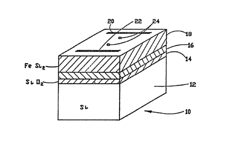
Figure 1 shows a perspective view of one
embodiment of the present invention being formed of
a semiconducting metal silicide shown generally by
the numeral 10. The substrate 12 is a silicon wafer
thermally oxidized to grow 1000 angstroms more or
less of insulating oxide 14. The oxide layer 14 is
then coated with several thousand angstroms of
polycrystalline silicon film 16. This
polycrystalline silicon film 16 is added commonly by
low pressure vapor deposition. ~ thin film of
metal, rhenium, is then added to the polycrystalline
silicon film 16 and then reacted by heating the
sample in an inert environment to react the metal
film with the polycrystalline silicon film 16 to
form a semiconducting metal silicide 18, rhenium
disilicide (ReSi2). Electrical contact with the
semiconducting metal silicide 18 is achieved by
depositing an aluminum or other conductive film 20,
22 and 24 on the semiçonducting metal silicide 18
which is then photolithographically patterned.
Other insulating substrates can be used and
coated with a silicon film. The metal deposition
technique can be evaporation or chemical vapor
deposition. Futhermore, the metal silicide film may
be formed by (simultaneous) codeposition of metal
and silicon.
Figure 6 shows a another embodiment of the
semiconductive metal silicide detector having a
6ubstrate 120 on top of which is formed a thin film
o~ semiconducting rhenium disilicide 180.
Conductive pads 121, 122 and 140 are formed on the
sur~ace of the semiconductive metal silicide thin
film 180.
-. . .
,, - :, : . . , ~
.. . ..
9- 13~6966
The metal can be chosen from the group
consisting of: iron, iridium, manganese, chromium,
rhenium, magnesium, calcium, barium or osmium. The
semiconducting metal silicides formed are: iron
disilicide (FeSi2), iridium silicide (IrSil 75),
manganese silicide (MnSi1 7), chromium disilicide
(CrSi2), rhenium disilicide (ReSi2), magnesium
silicide (Mg2Si), barium disilicide ~8aSi2~, calcium
silicide (Ca2Si) or osmium disilicide (OsSi2)
respectively.
The process for forming each semiconducting
metal silicide varies as to annealing temperature
and time. The chart 1 shown below shows some
combinations of time, temperature and a range of
thickness for the semiconducting metal silicides.
Each semiconducting metal silicide thus made has
been tested and shown to be a true semiconductor
which demonstrates useful radiation detection
properties based either on analysis of the data
showing the optical absorption edge for each
material together with measurements of electrical
resistivity as a function of temperature.
Element Temp.~Time (minutes) Thickness(Angstroms)
Chromium 900 C/120-1100 C/120 1000 - 13,000
Manganese 800 C/120-1000 C/60 1900 - 15,000
Iridium 750 C/120-850 C/120 1355 - 5,418
Rhenium 90o C/120307 - 768
Iron 900 C/120 700 - 3,200
. . .
CHART 1
The active silicide layer can be made by
depositing a thin film of the desired metal onto a
silicon wafer which has been polished and cleaned
for integrated circuit fabrication. It is important
to have a clean metal-silicon interface before
annealing. A~ter heating to the proper temperature
' ' : . ,,, -
. . .
..
: , : . ,:
-lo- 1 3269 66
and for the proper time, the metal film will react
with the silicon substrate to form semiconducting
metal silicide. The semiconducting metal silicide
film may also be grown on a polycrystalline silicon
surface.
For example, rhenium disilicide ~ReSi2) was
prepared by ion beam sputtering of rhenium film onto
1-0-0 polished silicon wafers. The semiconducting
metal silicide layer was grown by reaction of the
rhenium metal film with the silicon substrate at an
elevated temperature such as 900 degrees C in an
inert environment of flowing argon gas. The
substrate is ion-milled in vacuum immediately prior
to metal deposition.
Figure 2 illustrates a circuit that uses the
semiconductive rhenium disilicide detector of Figure
1. The conductive pads 20, 22 formed on the
semiconducting rhenium silicide layer shown in
Figure 1 are connected by wires 21, 23 to a constant
current source 50. Conductive pads 24 of Figure 1
are connected by wires 25, 27 to a voltmeter 60. A
source of infrared radiation 70 illuminates
semiconducting metal silicide infrared detector
device 10. The resistance of the semiconducting
metal silicide infrared detector device 10 drops as
it is exposed to infrared radiation so that the
voltage measured by voltmeter 60 drops as a function
of the intensity of infrared radiation from infrared
radiation source 70. An analog-to-digital converter
62 i8 shown receiving information from voltmeter 60
; for digitizing t~e output of the semiconducting
metal silicide infrared detector 10. ~lternatively,
a change in current in the presence of a constant
voltage across the detector device 10 can be
,
.,
~ . , i -
-: .: :' ' : .,
... i ~ ,
:
- ~. :; ~ .
-11- 132~36~
measured to determine the change in resistance of
device 10.
Figure 3 shows an array of infrared detector
devices of the type shown in Figure 1. The array
shown generally by the number 300 is formed of
semiconducting metal silicide infrared detector
devices 302. Each infrared detector device 302 has
leads 304 into which a constant current can be fed
from a current source (not shown). Each infrared
detector device 302 also has leads 306 from which
the voltage drop across the infrared detector device
can be measured or detected. The array 300 is grown
on a substrate 308 which can be formed of a wide
variety of materials including silicon. If silicon
is the chosen substrate, the entire array can be
formed monolithically. In that case, the leads 304,
306 would be formed on the substrate 308
phot~lt~ graph~ by techniques well known in the
semiconductor fabricating industry.
Figure 4 shows an integrated circuit 101 formed
of microprocessor circuitry 100 (or other VLSI
device) and a semiconducting metal silicide
infrared detector array 110 shown for the purposes
of illustration only as a separate element. One use
of such a device is incoming missile detection and
ranging. Currently, such combinations of infrared
detection and computer analy~is of the incoming
signals are performed by interconnecting discrete
devices or by using monolithic arrays of Schottky
barrier detectors. The discrete devices each
perform satisfactorily but are not as fast, compact,
low cost to make, or reliable as a single integrat~d
device. The Schottky barrier detectors have a low
guantum efficiency and are relatively slow devices.
' '' .'., :
' ~ . ' '
1326966
-12-
The potential speed difference is substantial,
p~rhaps loo times that of present devices.
Intrinsic semiconductor detectors have a higher
quantum efficiency than Schottky barrier detectors.
The quality of the electrical interconnects is an
important factor in the speed of the device.
Similarly, the integrated system is more rugged,
faster and more reliable than a hybrid system formed
of discrete devices. The net result is that such
devices could be hand held or easily portable. The
increased speed of data processing, the ruggedness
and reliability can be critical in military and
space use.
Figure 4 shows the array as a two dimensional
array of semiconducting metal silicide detectors 12
whose output is represented by the bundle of leads
112 which contain data fed to microprocessor
circuitry lO0. Microprocessor circuitry 100
fabricated on substrate 106 receives power through
20 leads 102 and transmit~ information via leads 104.
Additional data and control information may be
placed into the microprocessor by leads 108. The
entire integrated circuit 105 is fabricated on a
substrate 106 typically of silicon.
Figure 5 shows a bundle of optical fibers 200
which are aligned with and receive signals from a
mated array 210 of semiconducting metal silicide
sources 12. The direction of transmission can be
reversed so that the fiber optic bundle 200 transmit
radiation to an array of semiconducting metal
silicide detectors 12. While the sources can in
some cases operate as detectors, in practice devices
are optimized for each application as either sources
or detectors.
1326966
-13-
Figure 7 shows a linear array 309 of
semiconducting metal silicide detectors 313, 311 and
303 having leads 305 and 307 for receiving current
and for connecting to instruments for measuring
changed resistance, photocurrent or photovoltage.
The linear array 309 is mated with a matching array
of optical fibers 325 having, for example, three
fibers 203, 211 and 213 which align with
corresponding elements 303, 311 and 313 as shown in
the figure.
Figure 8 shows in detail a substrate 401 which
can be formed of either p- or n- type silicon and
has two layers of either n or p type doped
semiconducting metal silicide 402 and 404 formed
thereon. The upper and lower semiconducting metal
silicide layers must be oppositely doped material
and the substrate 401 can be opposite in doping to
the semiconducting metal silicide layer adjacent to
it as shown in Figure 8. Part of the upper
semiconducting metal silicide layer 406 is removed
to expose the surface 410 of the lower
semiconducting metal silicide layer 402. Conductive
contacts 40~ are formed on both surfaces 406 and 410
for permitting electrical connection to the
device. Current is injected at lead 413 and rcmoved
at lead 415 or vice versa for operation as a source,'
of electromagnetic radiation. When exposed to
electromagnetic radiation, the device may gcnerate a
photocurrent "i" or alternatively a photovoltage
between leads 413 and 415. Voltage/current sensor
circuit 420 is connected to leads 413, 415 to detect
the photovoltage/photocurrent and changes therein
due to the applied infrared radiation.
Figure 9 shows another embodiment in the form
. ... . .
'
- : . -
-14- 1326966
of a heterojunction device 500 having a silicon
substrate 501 and a semiconducting metal silicide
thin film 502. Conductive contacts 514 and 506 are
formed on the bottom of the substrate and the top of
the semiconducting metal silicide thin film,
respectively. Current is injected at lead 512 and
removed at lead 510 or vice versa for operation of
heterojunction device 500 as a source of
electromagnetic radiation. When exposed to
electromagnetic radiation, the heterojunction device
500 may generate a photocurrent "i" or alternatively
a photovoltage between leads 510 and 512.
Voltage/current sensor circuit 520 is connected to
1 e a d s 5 1 0 , 5 1 2 t o d e t e c t t h e
photovoltage/photocurrent and changes therein due to
the applied infrared radiation.
Figure 10 is a graph showing the experimentally
measured optical absorption coefficient for the
semiconducting rhenium disilicide as a function of
wavelength and confirms the infrared detection
capabilities of ReSi2 in these longer wavelengths.
Superimposed on the graph are atmospheric
transmission windows of infrared radiation 520, 521.
Certain optical fibers also transmit infrared
radiation in these longer wavelength ranges, and
NASA has also expressed an interest in extra-
terrestrial infrared instrumentation applications in
these longer wavelength ranges.
Existing silicon compatible intri~sic
semiconductor detectors can detect wavelengths up to
a range o~ about two miorons, while this rhenlum
disilicide detector can detect infrared radiation in
all practical long wavelengths up to about 1~
microns. Thus, this invention provides a silicon
: . . .~.~ . .
. : . ................. - . ~
,~ . . . ~ . . : ,.. ~ ; , :
1326966
-15-
compatible intrinsic semiconductor detector that can
detect infrared radiation transmitted through the
longer wavelength atmospheric transmission windows
o~ infrared radiation, and can be used with fiber
optics that transmit such longer wavelength
radiation. -
While a specific embodiment has been disclosed,
it is expected that those skilled in the art will
devise alternate embod;ments that fall within the
scope of the appended claims.
. ~ .... .
.~: . , .. " . : . ~
, . . . . .. . ..