Note: Descriptions are shown in the official language in which they were submitted.
-- 1 --
SYSTEM FOR SWITCHING FROM WORKING UNITS
TO STAND-BY UNITS
BACKGROUND OF THE INVENTION
1. Field of the Invention
The present invention re].ates to a control system
for switching between working units and stand-by
units, and more particularly, to a system wh.ich can
realize a change-over constitution between working
units and stand-by units in response to the degree of
importance of the working unit, especially in a
digital multiplex equipment having a plurality of
units for multiprocessing signals, such as
multiplexing or demultiplexing operations.
2. Description of the Related Arts
In recent semiconductor technology, a large
! member of circuits are integrated to form, for
example, a multiplexing portion or a demultiplexing
portion in a multiplex network; these integrated
circuits being mounted on a printed circuit board to
form a unit. A plurality of these units are contained
in one package, in accordance with the number of
multiplexing lines in use, to form a multiplexer unit
or a demultiplexer unit. Obviously, in such a unit-
using structure, a stand-by unit must be provided to
improve the reliability of the package, by switching
from a working unit to a stand-by unit when a fault
occurs in the working unit. In this dascription, the
term "working unit" denotes a unit currently in
operation~
SUMMARY OF THE INVENTION
A feature of one embodiment of the present
invention provides an improved switching system in
which the switching from a working unit to an
individual stand-by unit or to a common stand-by unit
is carried out in correspondence with the deyree of
.~ ~
1327~8~
-- 2 --
importance of the working unit.
In accordance with an embodiment of the present invention
there is provided a switching system for switching between at
least one unit in a working state and at least one stand-by unit
in a stand-by state, the system selectively operating each of the
at least one stand-by unit as one of an individual stand~by unit
and a common stand-by unit accessed by an individual switching
unit, comprisingD input/output lines for transmitting data;
individual units, each comprising one from among the individual
stand-by-unit and the individual switching unit, each individual
stand-by unit and each switching unit including first switches
connected to the input~ output lines; working units, each
including second switches operatively connected to the
input/output lines, each of the working units corresponding to
one of the individual units in a pair arrangement; failure
detection means for providing fault detection signals indicating
faults in the working units; and a control unit, operatively
connected to the worXing and individual units and the failure
detection means, for controlling switching between one of the
working units and the corresponding one of the individual units
based on the fault detection signals from the failure detection
mean~, upon occurrence of a failure in the one of the working
units, the second switches disconnecting the input/output lines
from the one of the working units, the first switches connecting
the input/output lines to the corresponding one of the individual
units and, when the corresponding one of the individual units is
the individual switching unit, the first switches connecting the
input/output lines to the common stand-by unit.
BRIEF DESCRIPTION OF THE DRAWINGS
Figure 1 is a functional diagram of a prior art multiplexer;
Figure 2 shows the connections ~or individual ~tand-by units
in the priqr art;
Figure 3 shows the connections for a common stand-by unit
in the prior art;
~r~3
~327~8~
- 2a -
Figures 4A, 4B and 4C are block diagrams showing embodiments
of the present invention, wherein Fig. 4A is for the case of . .
working units, individual stand-by units, and a common stand-by
unit, Fig. 4B is for the case of working units and individual
stand-by units, and Fig. 4C is for the case of working unit and
a common stand-by unit;
Figure 5 is a wiring diagram showing an arrangement of
working units and stand-by units relating to a back plate printed
circuit board;
Figure 6 shows a structure of a circuit for l-to-1 switch-
ing;
Figure 7 shows a structure of a circuit ~or 1-to-n switching
structure;
Figures 8A, 8B and 8C show examples of the switch circuit:
and
Figure g is a flow chart of an example of the operation of
the system according to the present invention.
DESCRIPTION OF THE PREFERRED EMBODIMENTS
In data communication, a multiplexer or a multiplexer unit
is provided in which a plurality of data transmission lines are
6~
~32708k
-- 3 --
multi~lexed to enable the forming of a faster data transmission
line, and this multiplexer possesses both multiplexing and
demultiplexing functions.
A multiplexer is conventionally used as shown in Fig. 1.
For example, data of 1,544 MB/sec is transmitted via four lines
to a first multiplexing circuit (e.g., M12), the output Gf which
is multiplexed to transmit data of 6.312 MB/sec to a second
multiplexing circuit (e.g., M23) via seven circuits. The seven
first multiplexing circuits and the second multiplexing circuit
form a multiplexer unit such as M13 MUX. Further, nine
multiplexer units are combined therewith to form a third
multiplexer unit. Then, twenty-eight lines of data are
multiple~ed by seven multiplexing circuits M23 to output data of
45 MB/sec, and further, via nine lines for data of 45 MB/sec,
multiplexing is carried out via data transmission lines to output
date (e.g. 405 MB/sec).
In general, the change-over operation or switching operation
between working units and stand-by units is carried out as
follows.
(1) l-to-l switching structure
This is a structure in which a stand~b~ unit is
provided for one working unit.
(2) n-to-l switching structure
This is a structure in which a stand-by unit is
provided for n working units to form an n to-l switching
structure.
The l-to-l switching structure is applied to a working
unit having a relatively high importance, and the n-to-l
switching structure is applied to a working unit having a
relatively low importance. A unit having a high importance is
one utilized, in particular, for an administrative office, a fire
department, military forces, and a police station or the like.
(3) n-to-m switching structure
This is a structure in which m stand-by units are
provided for n working units. This structure has an unavoidable
problem in that the switching structure between the working unit
and the stand-by unit is very complicated.
In a prior art switching technique between the workin~
~327084
-- 4 --
units and the stand-by units, stand by units are prepackaged in
accordance with the degree of importance of the working units;
i.e., the l-to-l nr n-to-l switching structure is formed.
Therefore, the switching structure must be designed and
manufactured to fit many kinds of systems. Moreover, even if the
working unit has a low importance, more stand-by units than
necessary must be packaged, and thus incurs a disadvantage of an
uneconomical structure. On the contrary, when the importance of
working units is high, each working unit must have a stand-by
unit appended thereto.
The connections for individual stand-by units and for common
stand by unit in the prior art are illustrated by Figs. 2 and 3.
In Fig. 2 the individual stand-by units are connected in
parallel with or in accordance with a plurality of working units
through input side switch elements SWI-l to SWI-n and output side
switch elements SWO-l to SWO-_, and a control circuit is
connected to each input side switch element and each output side
switch element.
In Fig. 3 a common stand-by unit is connected to a plurality
of working units through a plurality of input side gates SWI-l to
SWI-n and a plurality of output side gates SWO-l to SWO-n.
An embodiment of the present invention will be described in
detail with reference to the accompanying drawings.
Figure 4A is a block diagram showing an embodiment of the
present invention.
The switching system as shown in Fig. 4a is provided with
first, second and third accommodation regions.
The first region accommodates n having an input side
switching portion 2a and an output side switching portion 2b, and
provided for the respective working units 1-1 to l-n are n number
of stand-by units 3-1 to 3-n having an input side switching
portion 4a and an output side switching portion 4b.
The second region accommodate~ at least one common stand-by
unit 3A. The working units 1-1 to 1-_, the stand-by units 3-1 to
3-n, and the common stand-by unit 3A have the same structure.
When a multiplexer unit is formed, a plurality of input lines are
connected through switching portions to the input side, and a
plurality of output lines are connected through switching
132708~
portions to the output side.
Assuming that the working unit 1-1 has a high degree of
importance, then a stand-by unit 3-1 is provided for the working
unit 1-1 and the switching portions 2a and 4a are connected to
the input side, for example, to a plurality of input lines, while
the switching portions 2b and 4b are connected to the output
side, for example, to a multiplex transmission line. In
- ~ . 13270~4
this case the switching portions 2a, 2b, 4a, and 4b are
provided with a switching structure corresponding to the
structure of the input lines and the multiplex line.
A common stand-by unit 3A is accommodated in the
common stand-b~ unit region and a switchin~ unit 5
composed of only a switching portion is accommodated in
the stand-by unit region of the (n-l) of working units
1-2 to l-n. The input lines for each working unit 1-2
to l-n are connec~ed through a switching por~ion of the
switching unit 5 to the input side of a common stand-by
unit 3A, and a multiplex line for each working unit 1-2
to l-n is connected through a switching portion of the
switching unit 5 to the output side of the common
; stand-by unit 3A. In this case, the switching portion
of the switching unit 5 is responsive to the switching
portions 2a, 2b, 4a, and 4b of the working units 1-1 to
l-n and the stand-by units 3-1 to 3-n.
A control unit 6 receives fault detection data from
the working units 1-1 to l-n and the coxresponding
stand-by units, and outputs a switching signal for
controlling the switching portions 2a, 2br 4a, 4b and
the switching portion of ~he switching unit 5.
Since the stand-by unit 3-1 is accommodated for the
working unit 1~1, the working unit 1-1 has a l-to-l
structure for working unit-stand~by unit switching and
when a fault occurs in the working unit 1-1, connection
thereto of the input lines and a multiplex line is
switched to the stand-by unit 3-1. Connection of the
working units 1-2 to l-n is switched through the
3~ switching unit 5 to the common stand-by unit 3A.
Thereforet if (n - 1~ = m, an m-to-l working unit-
stand-by unit switching structure can be realized.
Thus, when a fault occurs in any one of the working
units 1~2 to l-n, connection of an input line and a
multiplex line o~ the working unit in which a fault has
occurred are switched to the common stana-by unit 3A by
the switching unit 5.
~.
- ` 1327~
-- 7 --
The individual stand-by portion of this embodiment
shows a case of an ~ndividual stand-by por~ion having a
high degree of importance wherein the stand-by units 3-1
to 3-n are a~co~modated for the working units 1-1 to l-n
and all of the working units 1-1 to l-n are formed by a
l-to-l working unit versus stand-by unit switching
structure. Therefore, the common stand-by unit 3A (as
shown in Fig. 4C) is omitted.
A common stand-by portion in Fig. 4A is accommodat~d
in the region of the stand-by unit for the working units
1-1 to l-n and the common stand-by unit 3A forms an
n-to-l switching structure between the working units and
the stand-by units.
Fig. 4B is a block diagram showing an alternative
embodiment of the present invention. In the figure, the
stand-by units 3-1 to 3-n which make a pair with the
respective working units are accommodated responsive to
the working units 1-1 to l-n, so all of the working
units 1 1 to l-n have a l-to-l working unit versus
stand-by unit switching structure. Therefore, a space
for the common stand-by unit 3A which is illustrated by
broken lines is not accommodated therewith.
A pair of working units 1-1 to l-n and stand-by
units 3-1 to 3 n are connected in the input sides and
output sides respectively. The stand-by uni~s 3-1 to
3-n and a common stand-by unit 3A are connected commonly
in the input sides and output sides. Of course, a
con~rol unit is provided.
Fig. 4C iq a block diagram showing an alternativ~
3Q embodiment of the present invention. In the figure, the
switching unit 5 is accommmodated in the accommodation
: region of the stand-by units responsive to the working
units 1-1 to l-n and further a common stand-by unit 3A
is accommodated therewith, so a n-to-l working unit
versus stand-by unit switching structure is formed. The
switching unit 5 which occupies n locations r~sponsive
to the working units 1-1 to l-n and a common stand-by
- 8 - 1327~8~
unit 3A are connected in the input side and the output
side each other. The working units 1-1 to l-n and the
switching unit 5 are connected each other in the input
side and the output side, respectively.
S Furthermore, a plurality of regions for accommodat-
ing the common stand-by unit 3A may be provided, and the
working units 1-1 to l-n may be divided into a plurality
of groups and a common stand-by unit 3A may be accommo-
dated for each groups to form an n-to-m switching struc-
ture between the working units and the stand-by units.
The foregoing described embodiments relate to a
multiplexer equipment, but can be also applied to a
demultiplexer equipment.
As can be understood from the above description, a
switching system for switching from a unit or units in a
working state to a unit or units in a stand-by ~tate is
provided as either individual stand-by units or as a
common stand-by unit, and an individual stand-by unit or
a switching unit can be accommodated so that it forms a
pair with a working unit and working unit or units which
ara connected to a switching unit, so that when a
failure of the working unit or units occurs, the unit or
units are automatically connected to a common stand-by
unit.
Further it can be seen that the working unit
consists of a plurality of working units, and the
switching to an individual stand-by unit and the
switching to a common stand-by unit can be selected
according to need.
3Q Moreover, each of the working units and stand-by
units is a multiplexing or demultiplexing operation unit
~` able to carry out a multiplexing opexation for a
plurality of data received through an input line to
output multiplexed data to an output line.
Regardin~ the switching system in accordance with
the present invention, it is undexstood that a switching
from worXing units to stand-by units can be carried out
` ~32708~
only by a working/stand-by control, regardless of the
individual stand-by connection or common stand-by
connection.
More particularly, the switching system for
switchin~ from a unit or units in a working state to a
unit or units in a stand-by state, in which the units in
a stand by state are provided as either individual
stand-by units or as a common stand~by unit, each of the
working units having a higher importance being provided
with an individual stand-by units and each of working
units having a lesser importance being provided with a
switching unit, a plurality of the working units having
a lesser importance being provided with a common stand-by
unit, and a control unit being provided for controlling
the switching from working unit~ to stand-by units based
on failure detection signals, whereby switching control
signals from the control unit are supplied to the
individual stand-by units or the switching units, and to
the common stand-by units so that the switching from
working units to the individual stand-by units or the
common stand-by unit is carried out.
In the case of demultiplexex equipment, a multipl0x
line is connected to the input side and a plurality o
transmission linas ar~ connected to the ou~put side~
This ma~ be also applied to repeatex equipment or the
like, and in that case, one transmission line i5
com1ected to both the input side and the output side.
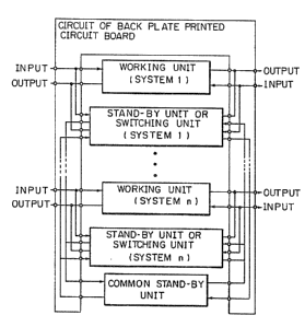
Figuxe 5 illustrates a wiring diagram of a back
pla~e printed circuit board, and shows a connection
diagram of a system Nv. l to a system No. n; the
relationship between working units, stand by units, and
a common stand-by unit is th~ same as in Fig. 4.
In the system according to the present invention,
it is possible to adopt a shelf structure in which each
stages of shelf plates are arranged perpendicular to the
back plates and side walis at both sides. A n~mber o~
unit or unit plates are guided on rail means of the
- lo- 1327~
shelf plates and stopped by the back plates. A plurality
of unit plates are inserted via guide means between
supporting connectors and mounted ver~ically on the back
board by means of a pair of connectors for supporting
the unit plates.
Figure 6 is a block diagram showing a l-to-l
switching control system as an embodiment in accordance
with the present invention.
Figure 7 is a block diagram showing a l-to-m
switching control system as an embodiment in accordance
with the present invention.
Fig. 8A is a block diagram of a high speed switch
element, Fig. 8B is a block diagram of a low speed
output switch employing a tri state integrated circuit,
and Fig. 8C is an example of a switch circuit as illus-
trated in Figs. 6 and 7.
Figure 9 is a flow chart showing a procedure of the
switching system. After ~he alarm detection of a
multiplexer or demultiplexer unit, a transmission line
monitoring instruction is sent to the stand-by unit and
swi~ch from a control unit, and a determination of
whether it is an external emergency or an internal
emergency is carried out. In the case of a line alarm,
a line alarm i5 displayed, and in the case of a unit
alarm, a switching instruction is sent to the working
unit and the stand-by unit from the control unit to
realize a switching operation.