Note: Descriptions are shown in the official language in which they were submitted.
- ; .
~327395
This invention relates to recording systems and more
particularly to systems for custom recording tape ca~settes or
other recording media by recording a number of specific
selections taken from a repertoire of selections which is stored
in a library or libraries.
For convenience of expression, this specification may refer
to music, tape, libraries, albums, and the like. However, it
should be understood that these and similar expressions should be
construed broadly enough to cover all equivalent items and
structures. For example, the r~corded information may be, not
only music, but also a recorded foreig~ language lesson, poetry,
telemetry, sound effects, or any other suitable items. The
recording media could be tape, r~cords, compact discs, optical
tracks on film, or the like. The ~library~ could be any suita~le
data base, including satellite, slave, or other distributed
libraries~ For ~xample, each recording company may have a remote
library of its musical selections which the inventive recorder
may reach via a telecommunication network. Tha term ~album" is
used herein to mean a certain batch amount of recorded
information items, ~e~ardless of whether the items are music,
voice, or some ot~er ~aterial. Long play records and tape
cassettes are exa~pl~s of albums; however, there may also be
other examples.
One example ot the invention is found in the recording
industry which issues nsingles~ and ~albumsn. If sin~les are
played, the listener hears exa~tly what he wants to hear, but he
has to continuously change records or tapes, which is a bother.
on the othsr hand, if ~n album is pl~ysd, the listaner usu~lly
lik~ on~ or two of th~ many selections which are recorded
thereon and is indifferent to or positively dislikes the
13273~5
remaining ~lect~ons in the album. The alternat~ve is to buy
expensive play back equipment which can pick one of many
selections in an album~ However, this, in effect, reduces the
album to one or two singles with all of the same problems that
singles present.
Within a few years after a recording is first made, it is
~cut out~ of the music catalogs which list the records that are
~hen being offered to the general public. After i~ becomes a
~cut out~, the musical selection may be included in albums a~ a
very low cost, and oft~n is offered as a special issue to a
select audience, such as the listeners of a TV sta~ion, but the
question of taste remains and not all of the records are
enjoyable to everyone. After a few more years, recorded music
tends to become unavailable at any cost. Then, those who are in
their nostalgia years do not have the option of playing a
recently acquired record containing the music of their youth.
Thus, there are many reasons why there is a need for a
system which enables one to select only his favorite music for
;.
inclusion in a custom recorded album. This way, everyone may
th~n have a customized album of selections of his own taste which
may b~ totally different from the albums which anyone else may
sèlect.
U.S. Patent ~,;10,917 has a capability of recording from a
master medium onto a slave medium but it does not provide a
random selection c~pability and does not provide a sufficient
flexibility. The structure of this patent can not rearrange~
edit, or modify the s~ored information items. It is strictly a
duplicator of recorded media.
A desirabie kind of master-slave recording system is one
30 which might eventually become almost as commonplace as record
stores. Still, the growth of such an industry may be relatively
slow: therefcrel the same system should also be adaptable to use
in a singl~ central location where custom record~d albums are
made for ~istribution via the mail.
132739~ ~
Accordingly, an ob~ect of thi~ invention is to provide new
and improved mean~ for and methods of distributing recorded
music. Here, an object is to provide systems for preparing
customized recorded albums containing only recorded information
selected by an individual.
In keeping with an aspect of the inventio~, these and other
o~jects are accomplished under the control of a microprocessor or
mini-computer. A master library, libraries, data base or storage
mediu~ contain recorded information which may originate from any
suitable source, such as phonograph records, tapes, sound tracks,
compa~t discs, telemetry sources, or the like. Each recorded
information item in the library is stored under its own address.
On read out, an operator keys in the addresses identifying the
selected recorded information item. The selected items are read
ol~t of the library medium and stored in a large capacity memory,
usually to provide a total of about forty-five minutes of
listening time. Then, all of the items are read out of that
large capacity memory and recorded at a hiqh speed onto a
suitable album size medium, such as a tape cassette, for example.
The various trans~ers of recorded information items from the
master storage to the recorded album, may be accomplished at a
high speed.
An embodiment ~ e the invantion is shown in the attached
drawings, wherein:
Fig. 1 is a bl~ck diagram of a first embodiment of the
inventive system for ~toring recorded information items, such as
musical selections, for example, in a master library;
Fig. 2 is a blo~k diagram of the inventive system for
retrieving recorded in~ormation items from the master library: \
Fig. 3 is a block diagram o~ a first embodiment of an
analog-to-digital module for converting the analog source music
into digital data for processing within the inventive system;
Fig. 3a is a block diagram of a low pass filter u~ed in the
ANDI and the DIAN modules;
~32739~
Fig. 3b indicates a clock rate caused roll off in the upper
frequency range o~ signals passing through said low pass filter;
Fig. 4 is a timing chart for the operation of the
analog-to-digital converter of Fig. 3;
Fig. 5 is a block diagram of a command control computer for
use in the circuit of Fig. l;
Fig. 6 is a block diagram of a master storage circuit for
use in Fig. l;
Fig. 7 is a block diagram of a master storage controller
circuit used in Fig. l;
Fig. 8 is a block diagram of a source media for use in Fig.
l;
Fi~. 9 is a block diagram of a first embodiment of a
digital-to-analog module ~or converting the digital data
processed by the inventive system into an analog form for
recording;
Fig. 10 is a timing diagram for the digital-to analog
converter of Fig. 5,
Fig. 11 is a destination controller for directing data taken
from the master li~rary to the album sized recordin~ medium;
Fig. 12 is a block diagram of an intermedi~te storage
circuit for buffer storing digital data relating to recorded
information items l~hich are read out of the master li~rary and
prior to its recording on the customized album;
Fig. 13 is a bLock diagram for a destination medium on whic~
the custom album is recorded;
Fig. 14 is a ~r~ph illustrating~ by best case and worst cas~
examples, a loss o~ ~idelity in a conventional prior art PCM
recording;
Fig. 15 is a similar graph showing how a second embodiment
of the inv~ntion improves the fidelity of the PCM signal;
Fig. 16 shows th~ high frequency end o~ a recorded
characterist~c curve that illustrates how the second e~bodiment
of th~ inven~ion improves the recorded fidelity:
-- 132739~
Fig. 17 is a block diagram of a second embodiment of the
analog-to-digital converter;
Fig. 18 ~s a block diagram of a second embodiment of a
di~it-to-analog converter;
Fig. 19 is a graph similar to Fig~ 15 showing how the
digital-to-analog circuit converts the digital signals back into
an analog signal with improved fidelity;
Fig. 20 is a timing chart for the converter of Fig. 18;
Fig. 21 is a block diagram of a destination controller for
use in the information retrieving system of Fig. 2;
Fig. 22 is a flow chart for the circuit of Fig. 21, showing
the state of the circuit responsive to a request control logic;
Fig. 23 is a flow chart for the circuit of Fig. 21, showing
the state of the circuit during bus control;
Fig. 24 is a block diagram of a master storage controller
for use in connection with the information retrieving circuit of
Fig. 21;
Fig. 25 is a flow chart showing the state of the circuit of
Fig7 24 in a request for control condition;
Fi~. 26 i~ a flow chart showing the state of the circuit of
Fig. 24 during bus control;
Fig. 27 is a block diagram showing the intermediate buffer
storage of Fig. 2, and
Fig. 28 is a flow chart showing the control over the random
access memory of F~. 26.
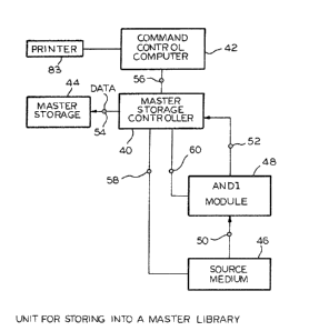
Fig. 1 shows .~ system which may be used to store or create a
master library con~ainin~ a repertoire of recorded information
items, such as musical selections, for example. The major parts
of this system are a central controller 40 operating in response
to a command control computer 42, a master storago medium 44, a
source medium 46, and an analog to digital conversion module 48.
The master storage medium 44 could be a laser disc, or the like.
Any suitable source medium 46 may be used such as records, tapes,
compact discs, optical tracks, or the like. Usually the
132739~
pertin~n~ pl~yback device at 46 has an analog output at 50 which
ANDI modul~ 48 converts into digital data. The digital data is
then transferred over a data input bus 52 and through storage
controller 40 to the master storage medium, via a data bu~ 54.
The storage of each recorded information item or selection is at
its own individually identified address location in the master
~torage medium 44. All of this happens in response to control
signals transmitted from a microprocessor or mini-computer 42
over control ~usses 56-60.
In Fig. 2, the selections stored in the maste,r storage
medium 44 are retrieved for asse~bly as an album which i~
recorded on any suitable destination medium 62, such as on a tape
cassette, for example, or the like. In greater detail, the
digital data taken from the master storage medium 44 are sent
over data bu~ 54, through the master storage controller 40, 3nd
bus 65 to an intermediate buffer storage circuit 64. After an
album amount of music (about forty-five minutes) is assembled in
., the intermediate storage circuit 64, it is sent over a data bus
66 to a di~ital-to-analog converter module (~DIANn) 68, from
which an analog signal is sent via bus 70 and recorded onto
mediu~ 62.
The data retrieval circuit (Fig. 2) is controlled by a
destination controlier 72, which is driven from the
microprocessor 42 via data bus 56 and master storage controller
40. Connected to the input~output ports of the destination
controller 72 are data request 74 bus, digital-to-analog co~trol
commands bus 76, destination medium control bus 78,
storage/retrieval address bus 80, and intermediate buffer storage
control bus 82.
39 In op~ration~ an operator simply appliec any suitable
recorded information in the source medium 46 (Fig. 1) by playing
a recording, tape, or the like. For example, the operator may
place a phonograph record on a turn table and play it back. The
command control computer 42 assign3 suitable addresses to each
recorded information item that ~9 played back an~ stored at 44.
T~is addre~s assignment may be don2 either automatically or in
response to operator entered command signals. Any suitable
printer 83 may print out a master list of recorded items and
their addresses in the master storage 44. An automatic address
assignment and print out is all done in approximately the same
manner that a word processor assigns document numbers and prints
out documents.
When a customer provides a list o~ ite~s for inclusion in a
single album, an operator consults the master list and enters the
indicated addresses on a keyboard 85 (Fig. 2) associated with the
command control computer 42. Resppnsive thereto, the master
storage controller 40 reads stored data out of the library or
libraries at master storage 44, where the digital data is that
stored under each selected address. That read out data is then
stored in the intermediate buffer storage circuit 64, at an
address selected by the destination controller 72. After all of
the digital data required to record an entire album is read from
the master storage circuit 44, the destination control 72, acting
responsive to computer 4~, causes the intermediate buffer storage
circuit 64 to transmits the entire album of data throug~ the
dlgital to analog "DIANn module 68 for storage on medium 62, such
storage being in an analog form.
In an alternative system, the intermediate buffer storage
memory 64 (Fig. 2) m~y have a much smaller capacity. Then, the
system may operate on a demand and fetch basis. That is, the
master storage circuit 44 reads out a burst of data which is put
into intermediat~ buffer storage at 64. In this alternative
~ystem, the resulting stored data immediately begins to be read
out of buffer 64 for storage at the destination medium ~2. As
the data is being so read out, the intermediate buffer storage 64
makes repeated demands for more data from the master storag~ 44.
As each demand is made, more data is fetched from the mastPr
storaqe ~ircuit 44, which is used to replenish the data being
1 32739S
taken ~rom th~ intermediat~ buffer storage and recorded in the
destination medium.
Figs. 3, 4 show the details of a first e~bodimen~ of the
~ANDI~ analog to digital module 48 and of the timing of the
module operation. This module 48 converts the analog
information, taken from the source medium 46 (Fig. 1) into the
digital data information that is processed and stored on the
master storage device 44.
More particularly, the analog signal which is taken fro~ a
record or tape, for example, enters the module 48 through input
port 84 and the input amplifier 86, which sets a uniform input
signal level by providing a suitable gain. Also amplifier 86
isolates the input port 84 from the next stage 88 which is a low
pass filter that rolls off or drops out the high frequencies.
The next stage is the sample and hold amplifier 90, which
holds a sample of the input signal at a constant level while the
analog-to-digital converter 94 is making its conversion. At 92,
a mode input control signal is applied to the sample and hold
amplifier 90 to select between the sample mode and the hold mode.
In the sample mode, amplifier 90 reads the input signal and
stores it inside the amplifier so. In the hold mode, it holds
the previously sampled voltage at a constant level, to prevent
the analog-to-digit~l converter 94 from trying to convert an
input signal with ~ level that is changing. In this particular
system, the sample and hold amplifier 90 has a very high oukput
impedance. The analog-to-digital converter 94 has a very low
input impedance. Thcrefore, to compensate for this, a buffer
stage 96 is coupled between these two devices. Of course, the
buffer may not be required if the impedances match.
The signal which reaches the analog-to-digital converter 94
is converted into digital data, such as a 16-bit digital word,
for example. When the analoq-to-digital converter 94 completes
the conversion, it strobes the digit~l word into ~ first-in
fixst-out (~FIFO~ buffer memory 98. This buffer store~ the
132739~
sampl0a in aligned rows, which may be 1,024 sample~ long, ~or
example. Then, on a first-in first-out basis, the command
control computer 42 (Figs. 1, 2) retrieves the stored data, on a
word by word basis. The read-out data i~ transmitted through the
digital buffer 100 to the master storage controller 40. Thi~
bu~fer storage enables the two systems to operate at speeds that
are not synchronized.
The bandwidth is selected at 99 by sample and filter clock
divisor signals sent over data bu~ 56 and received in the ANDI
module 48. In greater detail, two of the more important circuits
shown in this block diagram of Fi~. 3 are the timing generator
101 and the clock divider unit 102. The timing generator 101
places the sample and hold amplifier 90 in a particular mode and
starts the analog-to-digital converter 94. The timing generator
101 and the clock divider unit 102 are controlled via bus 56, by
a signal which is sent under the control of the master
microprccessor or minicomputer 42. In this particular
embodiment, the source clock 104 is a 5.64480 MHz crystal
oscillator which has an output that is an exact multiple of the
industry standard sampling rate. Other frequencies may be used
in other ~yste~s. Thus, the divider 102 provides a divided
sample rate which is equivalent to or any multiple of the
industry standard rate. The timing generator 101, in effect,
retimes the clock pulses divided by circuit 102 in order to
accommodate circuit ~elays, such as the finite time required for
a signal to transfer from the input of amplifier 86 to the input
of sample and hold _ircuit 90, for example.
The divided sa~ple clock rate pulse stream is sent from
clock divider unit 102 over wire 103 to drive the low pass filter
88.
In opexation, clock controlled low pass filter 88 (Fig. 3a)
switches a capacitor back and forth between its input and an
output. Its effect is to start a proces~ whereby the ~nalog
signal is divided into a plurality of pulses representing the
13273~
intelllg~ncQ in the analog signal. In greater dQtail, ths low
pass ~lter 88 lncludes a switched capacltor network 105 driven
from clock pulseB on wire 103, via divider circuit 106, and clock
generator 107. The divider circuit 106 may be set to divide by
1, 2, or 4. The switching circuit 105 alternately connects a
small capacitor to the input terminal ~IN~ and the output
terminal nOUT~. Fig. 3b shows a roll off characteristic wherein
the frequencies passing through the low pass filter circuit fall
off sharply after some frequency which is set by a ratio between
the frequency of the input signal divided by the frequency of
clock pulses delivered from the clock 107. Therefore, the roll
off frequency may be changed by changing the dividing factor of
the divider 106. This filter may be low pass filter LTC 1062
mad~ by Linear Technology Corporation of Milpitas, California
95035-7487.
Before the analog-to-di~ital conversion in converter 94, a
small segment of the analog signal is fed to a sample and hold
capacitor in circuit 90 where it is held lon~ enough to
accumulate a charge that represents the instantaneous amplitude
of a generally analog wave shape during that segment.
The timing requirements for the embodiment of the analog to
d~gital module that is shown in Fig. 3 can be seen in the timing
diagram~ of Fiq. 4. which are thought to be self explanatory.
The command control computer module 42 (Fig. 5) includes a
commercially available computer system 110 which should have
multi-user capabilit/. That is, the computer should be abIe to
sort and segregate data into a number of different categories.
Each of many clients and copyright owners has a separate record
keeping memory to make royalty accounting possible. Thus, as
each recorded information item is read out of the master storage,
a record company or other person owning the copyright on that
particular selection receives an accounting credit. In one
sy~te~, the command control co~puter was a four-user ~axicom/DL
computer with an 85-megabyteJ hard disk drive. This unit has a
- Trade Mark
132739~
genoral purpose parallel lnter~ac~ card 112 which send com~ands
and receiv~s responses from commands over the various data buses.
Any suitable interface circuit 112 may be provided to integrate
this computer into the over all system. In general, these
interface circuits meet the SCSI (small computer system
interface) standards.
The master storage cirouit 44 (Fig. 6) includes any suitable
recording device, such as a commercially available twelve or
fourteen inch laser read-write device 114 with a removabl~ disc.
One system used an Alcatel Thomson~Gigadisc. Data is stored on
and retrieved from the disc by the master storage circuit 44 in
response to standard industry commands. Both ~he data and the
master storage commands are sent over the data bus 54.
The master storage controller 40 (Fig. 7), uses custom -
software with a commercially available 32-bit central processor
unit 116 which may be a Motorola~MVME-130, for example. An SCSI
interface card 118, and a general purpose parallel interface card
120, interconnect the controller 40 with other circuits via
standard data ~uses.
The source medium 46 (Fig. 8) is any suitable commercially
available, studio quality, reel-to-reel player, phonograph disk
player, cassette player, CD disk player, or any other suitable
device 126 that can supply suitable audio output signals, usually
analog signals. Or~ce the source medium 46 has received its
command, regardless Oe whether it is "start", "stop~, "rewind"
etc ..., over the source medium control bus 58, it responds as
directed an~ sends analog output signals over the source medium
output bùs 50 to the next stage.
Under ths control of the command control computer 42, the
storage controller 40 selects the bandwidth. Then, controller 40
starts the source medium 46 by sending signals over the source
msdiu~ control bus 58. Once the master storage controller 40 has
started the source mediu~ 46, it begins r~ceiving sa~ples which
ar~ sent from the ANDI modul~ 48 over the input d~ta bu~ 52.
- Trade Mark
11
132739~
The~ s~mple~ are forwardsd through the bus 52 to the master
storag~ c~rcuit 44 by way of the data bus 54.
After the command control computer 42 commands a read-out,
controller 40 sets up the destination controller 72 (Fig. 2) by
way of the command bus 56. After the destination controller is
initialized, it begins a retrieve cycle in order to take data
from master storage circuit 44 by way of the master storage data
bus 54 and the SCSI interface card 118 (Fig. 7). The information
that is being received Prom master stora~e circuit 64 is sent
over the data bus 54 to the intermediate buffer storage circuit
64, where it is stored.
Figs. 9, 10 show details of a first embodiment of the
digital-to-analog (DIAN) module 68 and of the timing of the
module operations. This module 68 translates the digital data as
it is received from the destination controller circuit 72 (Fig.
2) into the analog information that is required for the
destination medium 62.
Th~ digital-to-analog conversion process starts with the
destination controller circuit 72 setting a clock divider unit
130 in the module of Fig. 9 to operate at the desired output
sample rate. The command signals that set the sample rate are
sent via the command control bus 76. After a period which is
long enough for this clock rate to stabilize, the destination
controller 72 (Fig. 2) starts the destination medium via bus 78.
The intermediate buf~er storage circuit 64 continuously sends
16-bit samples to th~ first-in first-out buffer circuit 132 ~Fi~.
9), over the data bus 66.
Two critical circuits in the digital-to-analog module (Fig.
9) are the timing generator 134 and the clock divider unit 130.
The timing generator retimes the divided clock pulses in order to
accom~odat~ the circuit delays. For example, therc is a circuit
delay that is re~uired ~or a signal to transfer from the FIF0
bu~er 132 to the converter 142, which the retime~ pulse
accommodates.
132739~
Tha master clock 136 ha a frequency of 5.64480 MHz in thls
embodimen~. This frequency is divided by the clock divider unit
130. The destination controller 72 sends a divisor control
signal to the clock divider unit 130 which is used to divide the
master clock pulse repetition rate. Likewise, the destination
controller also sends a divisor control signal over the command
control bus 76 and through circuit 130 to the low pass filter
140, which uses it as a filter clock frequency. The output of
the low pass filter 140 goes through an output buffer 146 in
order to drive the destination medium 62 via bus 70.
As the sa~ple clock pulse stream is sent to the timing
generator 134, it generates and sends a read pulse to the
first-in first-out buffer 132. Once this read pulse has been
sent, the data is read out of the first-in ~irst-out buffer 132
15 to the digital-to-analog converter 142. Converter 142 then
receives a start command from the timing generator 134, via wire
143, whereupon it ignores all other ~ata on its inputs and
converts the digital data word that it receives into an analog
output sample. The analog output signal travels through a buffer
20 stage 144 to low pass filter 140, which limits the output
frequency response of the system. Because the output sample
frequency may be changed for varying destination speeds, the low
pass filter 140 may be programmed to vary the roll off
frequencies, witho~lt requiring a revision of the software.
Fig. 10 show~- t~e ti~ing for the operation of digital to
analog converter of Fiq. 9. It is thought that this chart is
self explanatsry.
The details o. one emhodiment of the destination controller
72 are shown in Fig. 11 as including two 32-bit binary counters
30 150, i52 and a destination control latch 154~ The destination
control process be~ins with the master storage controller 40
(Fig. 2) storing, via the command bus 56, a start addres3 in the
32-bit binary counter 150. Destination controller 72 triggers
the digital-to-analog circuit 68 via the bus 7~ (Fig. 9). Then,
13
13273~S
data byt~s begin flowing from the ma5ter storage circuit 44 (Fig.
2) through the master storage controller 40 to intermediate
buffer storage circuit 64.
The intermediate buffer storage circuit 64 (Fig. 12) has a
module with a memory which consists of a large RAM array 156 and
a storage capacity of ninety-six or more megabytes. Data comes
in from the master storage controller 40 (Fig. 2~ via the data
bus 65 (Fig. 12) and is combined in circuit 158 with a 32-bit
storaqe address received from the destination controlled 72 by
way of the storage address bus 80. This combined data i5 then
stored in RAM 156 at the indicated address. Data is retrieved
from the RAM 156 in response to an address that is generated in
the destination controller 72 and sent over the retrieve address
bus 82. Once the address has been latched at circuit 160, data
is retrieved from the RAM array 156 and is sent to the DIAN
module 68 via the data bus 66.
Each time that the intermediate buffer storage circuit 64
receives a data byte, it also sends a strobe signal over part o~
the data bus 56 to the destination controller 72 (Fig. 2). This
strobe signal increments the counter 158 each time that a data
byte is stored into intermediate buffer storage circuit 64. At
this time, the new address is incremented and sent back from the
destination controller 72 to intermediate buffer storage circuit
64 via the address bus 80. This process continues until the
master storage con~r~ller 40 has sent all of its data bytes to
the intermediate buf~er storage, at which time it sends a sample
rate divisor to the digital-to-analog module 68 (Fig. 2) via the
command bus 56.
Once the sample rate has settled in the module 68 (Fig. 9),
destination controller 72 sends a destination medium control
start signal over the destination medium control bus 78 (Fig.
11). ~ssuming that the destination medium is a cassette
rerorder, it is started in a record mode by this signal. Then,
the destination ~ontroller circuit 72 sets up the int~rmediate
14
132739~
buffer storage circuit 64 (Fig. 12), starting a retriove address
routine via the command bus 82 and then enables the
digital-to-analog module 68. As they are ~eeded, the module 68
sends a data bytes request signal over the data request bus 74 to
the intermediate buffer storage circuit 64. Also, destination
controller 72 (Fig. 11) increments the retrieve address binary
counter 152, whic~ then sends the newly incremented address to
the intermediate buffer st~rage circuit 64 via the retrieve
address ~us 80. This process continues until all data have been
sent from intermediate buffer storage circuit 64, at which time
the master storage controller 40 (Fig. 1) stop~ the
digital-to-analog module sample rates, and also stops the
destination medium 62 (Figs. 2), via the destination medium
control bus 78. The tape recorder or other recording device
switches off.
When the recording is completed by the destination medium
62, the master storage controller 40 may send a nrewind~ or other
suitable command via the destination medium control bus 60 to end
the recording production.
The destination medium 62 (Fig. 2) may include any
commercially available duplica~or, and usually any suitable
cassette recorder, such as those sold under the trademarks
Infonix, Pentagon, etc .... The destination medium 62 receives
its command (regar~iless of whether they are "startn, nstop",
"rewindn etc ...~ over the destination medium control bus 78.
Once it has received its co~mand, the destination medium 62 then
records the audio si~nals which it receives over the destination
medium signal bus 70.
Fig. 14 is a graph which illustrates a pro~lem that the
prior art encountered when music is reduced to a pulse code
modulation (~PCM~) signal This graph plots time along a
horizontal axis and amplitude of sound along a vertical axis. A
mu~ical signal is shown which is much more complex than a similar
voice signal. This complexity occurs because there is an
~32739~
accumulation o~ musical instruments (trumpet , violins, drums,
bell~, etc) which together make a much greater variety of sounds
than a human voice can make.
~he P~M technique originated in telephony where ths highest
frequency leYel of the transmitted voice signal is about 3500
cps~ The work which was dona for telephony indicates that the
sample rate should be at least twice the highest frequency that
is to be encoded (i.e. sample at a frequency which is at least
around 7000 cps).
There are two problems when this~standard PC~ sample rate
(i.e. sample at twice the highest frequency) is applied to music.
First, a sine wave suitably approximates a voice signal as it is
transmitted over a telephone line, since the wave form of the
lower frequencies of a single human voice does not depart too far
from such a sine wave. ~owever, a sine wave does not provide an
adequate basis for a study of musical signals, filled with the
complex sounds of an orchestra, for example. Second, telephony
is interested in a low cost transmission o~ a signal, with only a
sufficient fidelity for (1) an easy understanding of the spoken
word and (2) a not too oPfensive overall sound, In music, a mere
understanding is not enough. There is a demand for complete
fidelity, at a quality standard which is much higher than the
quality which is required for simple speech.
To illustrate t~is point, Fig. 14 contains an analog wave
form 200 of music ~hich has been arbitrarily drawn to show that a
simple sine wave c~n not represent more than a bare minimum of
the available inte~liqence. Thus, telephony studies based on
sine waves are not ~dequate to teach how to encode musical
signals. Accordin~ly, the standard sampling rate at twice the
highest frequency is not adeguate for music.
In Fig. 14, the marks 212, 214 indicate the boundaries of a
sinqle one of many cyclically recurrinq time slots which have the
conventional relationship wherein sampling must be carried out at
twice the highest freguency that i~ to be reproduced. The
132739~
in~tantaneous amplitudes of the sample line 216 indicate a rough
approximation betwe~n the analog wave 200 and the sample wave
form 216 within the time slot 212, 214. The approximation occurs
because the volt/second content of the time slot pulses forming
lines 216, 228 generally coincide with the averages of the analog
wave ~orm. However, even a glance also reveals that thexe is
much intelligence in analog curve 200 which is completely lost in
the-sample curve 216.
Next, suppose that the analog wave form 200 is displaced
slightly relative to the time slot 212, 214 so that the sample
period coincides with peak values 220, 222 in the analos wave
200, instead of with some fairly randomly positioned mid-points
224, 226 on the analog wave 200. Now the sample wav~ form 228
results. A visual comparison of sample wave forms 216, 228
quicXly establishes that the sample wave 228 is a very poor
representation of the analog curve 200. For present purposes,
wave 216 may be called the nbestn case and wave form 228 may be
called the ~worst~ case.
The differences between (i.e. the spaces between) the
analog waveform 200 and the sample waveforms 216, 228 is known as
the ~sample error.~ The assumption has to be that the time slots
and an analog average will not always coincide with a resulting
worst case sampliny error (i.e. that the error will be that of
sample wave form 2~8 and not of sample wave form 216).
There~ore, audio systems should be designed to provide the best
possible results ~th the worst case wave form 228.
A little thought ~akes it clear that the sample error
increases with an increase in the frequency of sound represented
by the analog signal. Accordingly, the sample error may be
reduced by passing the analog wave 200 through a low pass filter
Or stated another way, if a filter eliminates the pea~s 220, 222,
223 the worst case sample wave form 228 becomes very close to the
sptimum sample wave form 216. However, the analog wava form
which ls being reproduced has already lost much o its character
17
132739~
by the low pa~s filtering. This low frequency filtering of the
analo~ wav~ ~orm 200 completely destroy~ the intelligence
represented by the peaks 220, 222, 223. That loss presents a new
set of problems for an audio reproduction system which is trying
to provide a higher fidelity. Among these problems is a
restriction of bandwidth for the recorded signal.
It is apparent that if the samples are taken more often
(i.e. if the sample rate of the time slot 212, 214 recurs at a
higher frequency), the sample will follow the analog signal more
closely. Howevar, it is very difficult for the engineer
designing a recorder to make a fairly arbitrary decision to
increase the sample rate since the industry standard time slot
repetition rate is now well established. If a
recording/reproducing system is designed to operate at a new and
different higher sampling rate, existing reproducing equipment
can not play back the recordings made at that new standard.
According to the second embodiment of this invention, a
sampling system is run at a very hi~h rate in order to track the
- analog signal more closely and with greater fidelity than is
possible under the industry standard. The results of this high
speed sampling are fed into a computer which calculates a
theoretical wave form, as it would appear at the standard
sampling rate, if it follows and approximates the original analo~
signal with the ~est cases wave form. Then, the PCM signals
which are sent to the recorder are based on the thPoretical
sampling wave for~n which is calculated and not on the samples
which are actually read off the analog signal.
In greater detai1, Fig. 15 shows the analog wave form 200
and sampling-time slot 212, 214, which are the same as the
correspondingly numbered analog wave form and time slot shown in
Fîg. 14. Thus, a ~ampling wave which conforms to this time slot
212, 214 has all of ~he characteristics of a standard sampling
wav~ which may be encoded and later play~d back on csnventionally
available rep~oducing equipment. On the other hand, in this
132739~
embodiment, tha sampling cixcuit i~.driven at a very high rate
(such as six~een times the standard sampling rate). As a result,
the analog signal is sampled fast enough to follow it very
closely: therefore, the analog ~ignal is represented much more
S faithfully. The high rate sampling periods are represented by
~X~ marks (one of which is 230), each sample having an amplitude
which fall on the analog signal.
From these high speed samples, a computer calculates the
volt/second content of pulses forming the sample wave form 232 or
234 which most closely represents the analog wave 200. The best
case sample wave form 232 in Fig. 15 is drawn to be substantially
the same as the best case wave form 216 in Fig. 14 since it is
the best case, it does change with the invention. ~owever, the
worst case wave form 234 for the invention is shifted from the
best case wave for~ 216 by the same amount that the prior art
worst case wave form 228 ls shifted from the best case wave form
216. By comparing the area between the two prior art sample wave
forms 216, 228 with the area between the two inventive sample
wave forms 232, 234, it is easily seen that, with the invention,
the worst case sample wave form 234 is much closer to the best
case sample wave form 232, than the worst case prior sample wave
form 228 is displaced from the best case sample wave form 216.
Accordingly, it is no longer a problem if the sampling tends to
coincide with extr~e peaks of the analoq signal, in the manner
that the samplin~ ~a~e 228 coincides with the extremes of the
peaks and valleys o~ the analog signal 200.
Fig. 16 is a ~raph which indicates the improved fidelity
high frequency end of the spectrum for the inventive recordinq
system, as compared with a prior art recording system, using the
s andard sampling rate. The frequency delivered by a recording
will rise at some low frequency, have a flat top, and fall off a~
some high frequency. Fig. 16 shows that, for the standard
system, the fall off is abrupt at about 20X. With the inventive
system, th~re is abou~ a 2d8 loss at 40K, and a ~dB loss at about
19
13273~
60K. While people can not actually hear at these high
frequencies, there i5 a psychological response thereto which
qreatly enhances the recorded sounds, especially in the ~noise~
range. (i.e. such things as drums, bells, etc.).
Fig. 17 shows a block diagram of a circuit for practicing
this embodiment of the invention. In~greater detail, a sample
clock input 240 receives cloc~ pulses at a suitable high
frequency repetition rate which enables a closer tracking of the
analog signal, as indicated by the X-marks 230 in Fig. 15. It is
thought that a sample rate which is sixteen times the normal
clock rate might be in order. When the sample enable lead 242 is
energized the clock divider circuit 244 responds to the clock
pulses and provides several output signals.
The analog signal appears at input terminal 246 and is
applied to a gain adjustment circuit 248 which brings all input
signals to a standard amplitude. Thereafter, the signals pass
through a buffer amplifier 250 which provides isolation. Two
sample and hold circuits 2~2, 254 are provided to operate
alternately since the inventive sample speed is too high for
response by components in a single sample and hold circuit havina
an acceptable level of precision of response. The sample and
~old circuits 252, 254 are alternately enabled under the control
of a sequence and selector circuit driven from the clock divider
circuit 244. The circuits for actually selecting these sample
and hold circuits is represented by the switches 258, 260, 2S8',
260'. The outputs ~ these sample and hold circuits 252, 254 ar~
applied to the input of an analog-to-digital converter 262.
The clock divider circuit 244 applies clock pulses to
sequence and selector circuit 256 and to the converter 262 at th~
high repetition rate of the sample clock 240. The pulses are
reshaped by pulse shaper 264. Tha high sample rate may be
sixteen times the standard sample rate.
The clock divider pu~ses a timing yenerator 266 to inform it
of the time conversion, and it groups the hiqh speed samples at
~32739~
thP standard rate. For example, at the suggested sixteen-to-one
time conversion, clock divider 244 pulse~ the nfirst~ terminal
268 on the first of each of sixteen sequential clock pulses and
pulses the "last~ terminal 270 on the sixteenth pulse,
immediately followed by a reset pulse 272 on the ~reset~
terminal. Thus, circuit 266 groups sixteen high speed samples
into one standard sample.
The analog-to-digital converter 262 converts each sample
pulse in response to a clock pulse transmitted through pulse
shaper 264 to the "Gon terminal. After each of the sixteen
samples in a group, the converter 262 sends a ~done~ signal to
the timing generator 266.
The clock divider 244 sends a four bit number to the ROM 274
for each of the sixteen samples applied to and encoded by
converter 262, to identify each of the sixteen high speed samples
in a group as it is then being received. This number causes the
ROM 274 to send a coefficient to an accumulator 276, where it is
used as a multipller. The coefficients in the ROM are put there
by a programmer who designs the ROM. For example, if all sixteen
pulses have the same weight, the multiplier is 1/16 for each high
speed sample pulse. On the other hand, if the circuit 276 takes
a trend into account, there may be different coefficients for
each high speed sample in the group. Thus, if the sample shows
that the sixteen high speed sample pulses form an envelope which
more or less follows a triangular analog curve, the coefficients
represent the area of a triangle. Another coefficient i5 used to
produce the area of a rectangle if the high speed samples have an
envelope which is a rectanqular curve within the sample area
represented by the group of sixteen high speed samples.
The analog-to-digital converter circuit 262 s~nds each of
~he digitally encoded pulses which represent the analog signal to
the accum~-lator 276. There, they are multiplied by t~e
coafficiant derived from th~ ROM 274 and then accumulat~d to
~ 21
1327~95
bring the sample signals into correspondence with the industry
standard sampling rate.
In greater detail, Fig. 15 has been drawn to show sixteen
X-marks 230 on the analog curve 200, within the standard sample
period 212, 214. The converter 262, (Fig. 17) converts each of
the high speed samples represented by these X-marks into a pulse
code, which i~ sent to accumulator 276. The accumula~or stores
the codes of the sixteen samples forming a group corresponding to
a standard time slot and computes the pulse code of a
hypothetical sample that best represents the analoq curve during
the standard time slot 212, 214.
The data latch circuit 278 is enabled periodically to gate
out the pulse code representing the hypothetical sample of the
standard time slot. This code may be recorded directly; or,
depending upon system needs, it may be transmitted to a FIFO
memory for ~uffer storage to enable a retiming of the code
pulses.
Each time that a hypothetical sample has been computed at
the standard rate, the timing generator pulses a "strobe~ lead
280 to inform associated equipment that a sample has been
completed and is coming to be recorded. That associated
equipment responds to the strobe by pulsing the acknowledge bus
282. The circuit is now ready to process the next sample.
The second embodiment of digital-to-analog module 68 is
substantially the inverse of the circuit shown in Fig. 17. In
this module, the coef~icient ROM 274 may play a more important
role since the sixteen high speed sample pulses may be given
different amplitudes, thereby more closely approximating the true
analog curve.
Details of the system for recovering the analog signal are
given in Figs. 18-28, which rslate to the construction of the
DIAN module 68 ~Fig. 2), the destination controller 72, and the
int~rmediate buffer storage circuit 64.
" 132739~
The DIAN (Fig. 18) is another embodiment of the DIAN module,
which iq shown in Fig. 9, and which may compute a more accurate
analog curve. More particularly, the digital-to-analog converter
circuit (~IAN~) of Fig. 18 is substantially the reverse of
analog-to-digital circuit ~ANDI~) o* Fig. 3. Each of these DIAN
converter circuits is also individually useful, aside from their
use in the inventive system. For example, the ANDI circuit could
be used as part o~ a recorder, and the DIAN could be used in a
playback system. However, these circuits are described herein as
being used together in a single syste~.
The oversampled output of the digital-to-analog module of
Fig. 18 almost eliminates the need for an output low-pass filter,
since the oversampled output does almost all of the filtration
itself, as indicated in Fig. 3b~ The DIAN action makes a very
high speed operation possible without requiring a switched
capacitor filter. Also, if it should become desirable to change
the output speed, say from 16X to 32X, the DIAN action tends to
eIiminate a need for low pass filters.
In Fig. 19, line-A represents the original analog wave form
which was the basis of the analog-to-digital conversion in Fig.
3. Therefore, ideally, this exact curve desired at the output of
the DIAN module. Line-B represents a stepped output curve which
a standard PCM converter would produce, based on the samples
taken at points 1, 2, 3, 4, and 5 in line-A of Fig. 19. Line-C
represents the computed analog output which is produced by the
DIAN module of Fig. 18. Line-C is created by computing sixteen
sample~ (each represented by a dot) which are at points that are
evenly distributed along segments of a sine wave which are most
likely to represent the changes between the successive points 1
and 5.
In greater detail, the DIAN (Fig. 18~ receives the digital
or stepped signal represented by line B; however, it is
comple~ely obvious that the analoq signal did not have the
stepped wave with sguare corners at 1, 2, 3, 4, 5. Th~re was a
132739~
relatively smooth curve extending between these successive
points. A8 explained above, a simple sine wave does not
approximate a continuous flow of an entire analog musical
selection in the sense that it approximates a human voice for
telephonic communications. However, it is much bet~er than a
square wave and for the brief time represented by points 1, 2;
2, 3; ... 4, 5, it does approximate music. Thus, in the short
distance between points 1, 2 of Fig. 19, segments of a sine wave
are superior, as compared to the approximation of the square wave
lo B.
Accordingly, the circuit in the inventive system looks at
points 1, 2 on curve B and computes sixteen points (shown by dots
on curve C) evenly spaced between the sampled points 1, 2. In an
alternative embodiment, the computer calculates a segment of a
sine wave which would most likely fit the change represented by
points 1, 2. Next, the circuit looks at the change represented
by points 2, 3, and computes sixteen points which are evenly
spaced to this next point or which represent a segment of a sine
wave which most approximates the change. In one embodiment the
calculated analog wave is iinear between the points 1, 2: 2, 3:
etc. In the other embodiment, the segment of the sine wave which
was computed for the change between points 1, 2, and the next
computations for two segments of a sine wave curve most likely to
have occurred between points 3, 4 and 4, 5 form the analog curve.
Thus, in either embodiment and considering the differences
between the two embodiments, the DIAN converter, in effect, draws
a "most probable" curve which fits the leading corners of the
successive sguare wave pulses stored in the intermediate buffer
storage circuit 64.
8y using this process, a wave form may be computed which is
a more faithful duplication of the original analog wavs form.
Since the computed waveform is smoother than the conventional
digital curve, it reduces the demands upon the low pass output
24
X
~ 13273~
filter, thu~ bot~ improving the performance and reducing the
complexity of the circuit.
The operation of the DIAN module of Fig. 18 is coordinated
by clock signals which are multiplied by sixteen and applied
through timing generator 348. This clocking system is similar to
the clocking system that is shown at 244 in Fig. 17.
In greater detail, the sample data is received from the
intermediate buffer storage circuit 64 (Fig. 2), via data bus 66
(Fig. 18), which is the same as bus 66 shown in Fig. 2. ThiC
sample data is latched in the input latch 352 (Fig. 18) on the
first sample clock pulse that is received via wire 76 from the
destination controller 72 (Fig. 2). Then, subtractor 356
subtracts the output signal of the last sample latch 354 from the
present signal supplied by the input latch 352. The difference
resulting from this subtraction is the delta modulation or the
change in signal (points l, 2 or 2, 3 ... in Fig. l9), which is
- then latched on the output of thP subtractor unit 356. This
difference or change signal is divided by sixteen at 357 and
applied to accumulator 358.
In the accumulator 358 (Fig. 18), the output of the
subtractor 356 is added sixteen times to the last sample data.
Each one of those sixteen newly computed samples is sent to the
digital-to-analog converter 360 where it is converted into an
analog information signal. This analog information signal is
then sent through the lowpass filter 362 to the output buffer
364, which produces the output analog signal and forwards it over
wire 76 to destination medium circuit 62 in Fig. 2. Fig. 20 is a
self-explanatory series o~ time related pulses which show the
timing sf the cirouit of Fig. 18.
The destination controller 72 (Fig. 21) is an alternative
embodiment of the destination controller 72 of Fig. 2. The
destination controller 72 ~Fig. 21~ uses a control processor 370
which m~y be a micro processor or a minicomputer that controls a
plurality of DIAN modules 68, each o~ whic~ may be in Figs. 2 or
2~
' X
~ 1327395
18. Ea h DIAN module has access through a first-in-first-out
buffer memory 368 to a byte un~tacker 380 which converts ~he bit
transmission stream between serial and parallel streams in order
to take data from memory and transmit it over a data bus. The
control processor 370 also drives address generators 372-376
which increment to successively call up the data store in memory
and to transmit it through the DIAN modules 68 to the outgoing
signal buses.
Assuming that the inventive system is used to record a
conventional audio cassette, there are A and B tracks, each with
a left and a right channel to give stereo sound. If so, the DIAN
#1 (Fig. 21) provides the left channel for the A track, as
indicated on the left-hand edge of Fig. 21 by the notation ~A~.
The DIAN #2 provides the right channel for the A track AR. The
DIAN #N provides the right channel for the B track, BR. Another
DIAN module (not shown) provides the left channel for the B
track. All of these channels correspond to wire 70 in Fig. 2.
The input signals arrive at the intermediate buffer storage
circuit 64 via wire 65. Thus, the signal path is traced from
wire 65, through intermediate buffer storage circuit 64, data
latch 385, byte unstacker 380, a FIFO memory, a DIAN modula, and
conductors 70.
In greater detail, a command to reproduce recorded
information is received over command bus 56, which also appears
in Fig. 2. This command is fed into the control processor 370
(Fig. 21), whereupon the control processor 370 sets the
appropriate starting addresses for each of the address generators
372-376, associated with the DIAN modules 68. After the
addresses are set, processor 370 selects the direction in which
the address counts increment in the address generators and thus
the directions in which the bytes are r~ad out. This ability to
provide a selected one o~ bidirectional read outs enabl~s the
system to playback the recorded information in both the forward
and reverse directions. Thus, the recorded destination msdium
~6
; ~3273~
may bo recorded in either a backward or a forward direction.
Stated another way, the conventional audio tape cassette has
tracks A and B which are played back while the tape moves in
opposite directions. In this example, DIAN modules #1, 2 read
out in a forward direction while DIAN module #N (and another not
shown~ read out in an opposite direction. By reading data from
memory in bidirections, the invention records track A from
start-to-finish and track B from finish to start. The consumer
plays side A while the tape moves in one direction and then turns
over the cassette and plays side B while the tape move~ in the
opposite dixection. Thus, the invention may read bidirectionally
out of memory in order to record both tracks on one pass.
After the address and direction selections are completed,
the control processor 370 starts the destination medium to moving
and enables the operation of appropriate DIAN modules ~8. Once a
DIAN module is enabled, it requests data from the request control
logic 378. The request control logic 378 determines the priority
o~ and selects between the requesting DIAN modules. Then, logic
controller 378 selects the direction in which the bytes are to be~
read out of memory by the byte unstacker 380 and requests data
from the bu~ control logic circuit 3~2. This state i maintained
until the ~done" signal is returned by bus control logic circuit
382. The ~donen signal tells the request control logic circuit
378 that all of the data bytes have been read from a RAM (Random
Access Memory) in the intermediate buffer storage circuit 64
(Fig. 2), the read out control being accomplished via buses 80
and 82. At this point, the request control logic 378 waits for
the ~unstack-done" command from byte unstacker 380.
Byte~by-byte, the byte unstacker 3~0 writes the data readou~
over buses 80 and ~2 through a FIFO memory 368 and into the
appropriate ~IAN module 68. When all bytes have been unstacked,
byte-unstarker 380 send~ an unstack done signal to reque~t
control loglc 378, thereby indicating a completion of the readout
of the recorded information. Request control l~gic ~78 then
~327~9~
count~ one address as having been done in the requesting DIAN
module. From this address, the address generator m~y either
count up or count down depending on the direction selected by the
control processor 370 and given to the address generators
372-376. At this point, the re~uest control logic circuit 376
sends an acknowledge pulse to the requesting DIAN module, which
then terminates a cycle.
This data read out cycle repeats continuously until the
destination medium has been completely recorded. Then, the
control processor 370 stops the destination medium by sending a
- signal over bus 78 and simultaneously inhibits the DIAN modules
that were being used. This timing, as described above, is set
forth in the flow chart of Fig. 22.
When the bus control logic circuit 382 receives a request
from request control logic 378, it initiates a read cycle,
responsive to signals sent over buses 80 and 82 via the read and
- output enable lines. Then, logic circuit 382 strobes the line
which causes the intermediate buffer storage circuit 64 to read
stored information from memory. Thi~ state is maintained until
the buffer memory storage circuit has terminated its read cycle,
which is indicated by a Ndone~ puls~ sent from the int~rmediate
buf~er storage circuit to bus control logic circuit 382. Bus
control logic 38~ then releases the read, write, strobe, and
output enable lines. A signal is sent to the request control
logic circuit 378 to indicate that the cycle is done, the signal
being sent via the done line. This state i5 maintained until the
request control logic circuit 378 releases the request line nREQ"
extending to bus control logic circuit ~82. The sequence of
avents followed by the bus control logic circuit 382 is set forth
in the flow diagram or Fig. 23.
Fi~. 24 shows a ~econd embodiment of a master storage
controller which serves ~s item 40 in Fig. 2, and includes
intermediat~ buffer storage circuit 64.
~ 28
1327395
The master storage ~ontroller is similar to the destination
controller of ~ig. 21 ln that it is controlled by the
microprocessor or minicomputer 370 and request control logic 378.
The logic circuit 378 has access to a plurality of master storage
devices 386 which fit into the overall circuit at 44 (Fig. 2).
The byte stacker 390 converts between parallel and serial data
transmission, taking data from storage and sending i~ over a line
to the intermediate buffer storage. Again, the data may be read
out of storage under the control of address generator circuits.
The recorded information or audio signals are taken from the
master storage devices 386, which may be disks recorded by a
laser beam. There may be many such master storage disks for
storing information in order to provide greater ~apacity. The
audio siqnal path may be traced from the master storage devices
through by~e stacker 390, data drivers 391, bus 56, and
intermediate buffer storage circuit 64 to an output bus 66.
In greater detail, the command to retrieve data is received
via command bus 56 (Fig. 24) and stored in the control processor
370, whereupon it sets tho appropriate starting addresses in each
of the address generators 372-378 which are individually
associated with each master storage device 386. The starting
address is relative to the placement of music on the destination
medium. Then, the control processor 370 resets all master
storage FIFO ~first in, first out) buffer memories 388 to be sure
that no stray data is in them.
Once this process is completed the control processor 370
begins to send retrieve data commands to the master storage units
386. When a master storage unit ~eginY to read data, it also
latches the data, byte by-byte, into its associated FIFO bu~fer
memory 388. As each ~IFO bu~fer memory reaches its half-~ull
state, it requests service from the request control logic circuit
378. The request control logic circuit 378 determines priority
among the servica requesting FIFO device~. T~n it sends an
identi~ica~ion of the FIFQ ~evice with the highe~t currsnt
29
132739~
priority to the byte ~tacker 390, and also sends a start-to-stack
signal.
Byte-by byte, the byte-stacker 390 reads out data fro~ the
FIF0 buffers 388 and latches them into its internal data
register. After all bytes have been stacked, the byte stacker
390 sends the stack done signal to request control logic circuit
378, to indicate the completion of the readout. Request control
logic circuit 378 then sends a request signal REQ to bus control
logic circuit 382. This state is maintained until the done
signal is returned from bus control logic circuit 382, to
indicate to the request control logic circuit 378 that the data
bytes have been written into a RAM in intermediate buffer storage
via buses 80 and 82.
Then, request control logic 378 increments the storage
address counter for the requesting one of the master storag~
devices 386. This cycle continues until all of the required data
is read from the master storage devices. The timing for Fig. 24
is detailed in the flow chart of Fig. 25.
The detailed disclosure of the intermediate buffer storage
circuit 64 is found in Fig. 27, which is primarily a random
access memory (~AM) with peripheral control circuits. The
recorded information or audio signals enter at 65 and leave at 66
in the upper left corner of the figure. During the period while
the signals are in the intermediate buffer storage circuit 64,
they are stored in RAM array 400. The remainder of Fig. 27 is
devoted to control circuits.
More particularly, when the bus control logic circuit 382
(Fig. 24) receives a request fxom request control logic circuit
378, it initiates a write to memory cycle by sending writ~ and
bus enable signals over via buses 80 and 82. Then, bu~ cont-:ol
logic 382 pulses the strobe line in bu 82, which causes the
int~rmsdiate buf~er to write into memory. This writ~ state is
maintalned until the int~rmedi~t~ buffer storage circuit
tsrminate~ its read cycl~ w~ich is indicat~d by a don~ pul~e
X 30
1327395
which is sent to bus control logic circuit 382. Responsive
thereto, the bu3 control logic releases the read, write, strobe
and bus enable lines and indicates to request control logic
circuit 378 that the cycle is done. This state is maintained
until request control logic circuit 378 releases its request
line. This sequence of events for the bus control logic circuit
382 is set forth in the flow chart of Fig. 25.
The intermediate buf~er storage circuit (Fig. 27) includes a
state control circuit 390, a refresh control timer 392, an
address decoder 394, address drivers 396, data and control
drivers 398, and a large array of RAM chips 400. The state
control logic circuit 390 waits for a command strobe pulse from
bus control logic 382 which is transmitted via the data buses.
If the command strobe pulse is given and a board select signal is
received from the address decoder 394, a particular ~emory board
is enabled in the RAM array 400. The state control logic circuit
390 then checks for the presence of a valid read or write pulse.
If it is a valid read signal, the address received from the
address bus is latched and the row address is sent to the
addressed RAM in array 400. The addressed row is strobed via the
address strobe wire (RAS~ and the control decoder and drive
circuit 398.
The control drive circuit 398 determines which of four ban~s
of RAM chips is being requested by bus control logic 382, and
gives an appropriate RAS signal. Next, state control logic
circuit 390 gives a signal over the MUX line to change th~
address line drivers to the column address. The selected column
address line (CAS) is strobed thxough the control drive circuit
398. The control decoders in circuit 398 then give the
appropriate CAS signal. After the RAM acces~ time has passed,
tha data returning from the RAM array is latched into the data
latches 396. The done signal is given to the bu5 control logic
3~2 that is then requesting t~s data. A r~resh cycle is
inserted to retain the data in the RAM chips. ~hi~ also resets
1327395
timer 392 to prevent a board generated refresh. After the
refresh cycle is complete, th~ refresh timer 394 is reset. Tha
command strobe is released, along with all data bus drivers. The
circuit has now returned to its idle state.
If a write command is received via the data busea, an
address is latched in address decoder 394. The control drive
¢ircuit 398 sends data and a row address to the RAM array 400,
along with the row address strobe signal (RAS). Then, c~ntrol
drive circuit 398 sends the column address to the RAM array along
with an address strobe (CAS) and waits for a period equal to the
write time of the RAM. After completion of the write cycle, the
done command is sent to the requesting control logic. A refresh
cycle is added to retain the memory. After the refresh cycle is
complete, the refresh timer is reset and the command strobe is
released, along with all data bus drivers. The circuit returns
again to the idle state.
The refresh control timer ~92 waits for a predetermined
period of time after either a read or write request is received.
If no RAM access occurs, the refresh control timer 392 requests
the state control logic circuit 390 to issue a refresh cycle
signal. The refresh timer maintains a continued storage of the
data in the RAM chips.
A suitable RAM chip for use in this system is a 1 megabit
RAM chip such as that manufactured by the Toshiba Corporation and
known as a type TC511000. ~ecause of the high data transfer rate
which is possible with this form of multiple master storage
devices, a RAM chip access time of lO0 nanoseconds or shorter may
be used. Fig. 28 is a flow chart which gi~e3 the timing for the
intermediate ~uffer storage circuit of Fi~. 27.
Those who are skilled in ~he art will readily perceiv~ how
to modify th2 system. Therefore, the appended claims ar~ to be
construed to cover all equivalent structures which fall within
the true 5~0pe and spirit of the invention.