Note: Descriptions are shown in the official language in which they were submitted.
132764~
BACKGROUND OF THE INVENTION
1. Field of th~ Inventi()n.
Ths invention relates to the field of converting RGB signals into a composite
video signal, and its use in video overlays.
2. Prior Art.
Some commercially available computers, particularly personal computers,
provide circuitry which permits the merger of a composite video signal (e.g., NTSC
signal, more specifically Proposed Standard ElA RS-170A) with a computer
generated video graphics display, typically red, green, blue (RGB) signals. The
RGB signals may represent a video overlay such as text intended to be displayed
with the eomposite video signal. In a typical application an NTSC signal from a
broadcasting station, video disk or tape, or other source of a composite video
signal is merged with the signal representing the video overlay to provide, for
exampls, titles or subtitles over a background image represented by ths composite
signal.
OltQn, in the prior art, the signal representing the overlay image is storad in
a frame buffer. The portion of this overlay image in which the background image
from thls composite signal is to show thr~ugh is assigned a ~key color~ in tha buffer
which is distinct from any other color in the overlay image. Th~s buffer is thenscannlsd out synchronously with the composite video signal and ~he contents of
the buffer are compared, pixel by pixel, with the ~key color~ When the comparator
indicates that the porlion of thls buffer being scanned out contains the ~key color~,
a switch sel~cts the composite video signal to be the output signal. On the othar
hand, when other than the ~key color~ is scanned in the buffer (indicating that the
overlay irnage is being scanned) a signal from the comparator (key or keying
signal) causlss the switch to select thls contents of the buffer. This arrangement
: ` '
13276~8
permits the overlay image to be shown in all colors which the buf~er can store,
except for the ~key color~.
The frame buffer stores the overlay signal in digital torm (e.g., RGB or an
index to an RGB lookup table). The RGB signal is converted to a composite
5 overlay signal be~ore being coupled to ths switch, thus, the switch selects
between first and second analog signals. In another prior art arrangem~nt, the
composite video signal is converted to an RGB signal and th3 switch selects
between first and second RGB signals.
Commercially available integrated circuits are used to perform the above
10 described functions, such as MC 1378 and TDA 3301, both manufactured by
Motorola Semiconductor, Inc. Phase locked loops are used to synchronize the
scanning of the frame buffer with the composite video signal.
In many applications it is desirable to provide both merged RGB signals and
a merged composite video signal. This a110ws a user to record the composRe
15 video signal while monitoring the merged' images on an RGB monitor. One prior art
circuit for providing both output signals first converts the composite video into an
RGB signal and then merges two RGB signals. Ths results of this merger provide
first output RGB signals. A second composite output signal is provided by
converting the merged RGB signal into a composite video signal. This
20 arrangement provides a relativeiy poor second video output signal that results
from the second conversion~ Note that thers is, Tn effect, a ~serial" double
conv~rsion, and the second conversion provides relatively poor video because
there is unavoidable signal distortion from sach conversion step~ As will ba seen
with the present invention a double merging (not a double, serial conversion) is25 used to soive this problem and ther~by providing both high quality RGB and
composRe signal outputs~
- 132764~
Video artifacts are known to occur where computer generated images are
displayed on composite vid~o monitors. These arti~acts are caused in part by high
fre~uency video signals ~chroma crosstalk~ that occur at ths color ref~rence
fre~uency of 3.58MHz for NTSC signals. There are numerous filters used that
5 attempt to remove these artifacts. Oflen, a 3.58MHz notch filter is used to prefilter
the luminance component of an NTSC signal~ Applicant believes that lowpass
fiRers may be used in the prior art to remove all chroma signals, for exanlple,
above 3.0MHz. This eliminates the ar~ifacts but at the cost of destroying some of
the image sharpness.
R has been found that when tha frequoncy of tha dot clock associatcd with
RGB signals is not a harmonic of tho color reference frequency, color artifacts
appear when the signal is converted to composite video despite tho presence of a3.58MH2 notch filter. The present inve~tion solves this problem by using
a~dWonal notch fllters including notch filters to filter the keying signal.
; . ... . ... , . . . . .. .. ... . . . . ~
SUMMARY OF THE INVENTION 13 2 7 6 4 8
An improvement in an apparatus which converts RGB signals into a
composite video signal is disclosed. Notch filters are used centered at certain
5 frequencies. These frequ~ncies are equal to the dot clock frequency of the RGBsignal divided by integers provided that thQ frequency resulting from this division
~alls within the chroma subcarrier spectrum.
This improvement is used in an apparatus ~or providing video output signals
containing a composite video signal merged with ~irst RGB video overlay signals.10 A keying signal generation means provides a keying signal indicating when theimage represented by the video overlay signal overlies the image represented by
the composite video signal. A first converter converts the video composite signal
into second RGB signals. A second converter is used to convert the first RGB
signals into a composite overlay signal using notch filters to ~iRer the luminance
15 signal in the conversion process. Merging occurs in both a first and a secondswitch A first switch under control of the keying signal selects between the first
and second RGB signals. In a second switch the keying signal, filtered by notch
filters, is used to select between the composite video s;gnal and 1he composite
overlay signal.
Accordingly, in one aqpect the present invention resides in
~n apparatus for c~nverting red, green and blue (RGB) video
signals having a dot ~requency of M into a composite video signal having a
color referenc~ frequency N, where ~1 is not a harmonic of N, said apparatus
having terminals for receiving filters for at least one of the components Y, R-Y
and B-Y of the composit~ video signal, where Y is the luminance component of
the composite video signal, an improvement comprising:
a filter coupled to receive and filter said luminance component of said
composite video signal, said filter having a frequency characteristic which has a
notch center~d at a frequency approximately equal to M divided by an integer,
and where said frequency is within thl3 chroma subcarrier spectrum of said
composite video signal.
:: '
4 ~:
`` 1327648
In another aspect, the pre~ent lnvention resid~s in an
apparatus for convorting an RG~ video ~ignal having a dot
frequency of approximately 12.272 MHz into a composite video signal having a
color reference frequency of approximately 3.58 MHz, said apparatus having
terminals for receiving filters for at least one of the components Y, R-Y and B-Y
of 1he composite video signal, where Y is the luminance component of the
composite video signal, an improvement comprising:
a first notch filter coupled to receive and filter said luminance component
of said composite video signal, said nrst notch nlter having a notch centered at
approximalely 4~09 MHz;
a second notch filter coupled to receive and filter said luminance
component of said composite vidso signal, said second notch filter having a
notch c~ntered at a frequency of approximately 3.07 MHz.
Other aspect3 o~ the present invention will be apparent
fro~ the detailed description of the invention.
.. ., .:.. , . . . ... . .. :, ., . .: . . .,. , . . " , - . .:
- - - . .
B --F DESCRIPTION OIF THE DRAWINGS 13 2 7 6 4 8
Flgure 1 is an electrical schematic of the presently preferred embodiment
of the invention.
Figure 2 is a general block diagram illustrating one aspect of the present
invention.
FigurQ 3a is a flow diagram illustrating the steps used to implement one
10 aspect of the present invention~
Figure 3b is a flow diagram illustrating a specific example for dat~rmining
the freiquency of notches tor notch fiiters based on the flow diagram of Figure 2a~
, . . ................. ' . . . . ~ :, .
", .~;... ..
D. . AILED DESCRlPTlOt~ OF THE PRESENT INVENTION 1 3 2 7 6 ~ 8
The presently preferre!d embodiment of the present invention is an
apparatus for providing output video signals which represent a composite video
5 signal merged with a video overlay signal. This preferred embodiment as well as
other aspects of the present invention are described below. In the following
description numerous specific details are set forth such as specific ~requencies in
order to provide a thorough understanding of the present invantion. It will be
obvious, however, to one skilled in the art that these specific details need not be
10 employed to practice the prèsent invention. In other instances, well-known
cirwits are shown in block diagram form in ordar not to unnacessarily obscure the
present invention.
Referring first to Figur~ 2, a computer 53 is shown which includes a memory
or buffer 54~ This computer may bQ any one of sQveral comm~rcially available
15 computers including personal computers. Buffer 54 is typically the random-
access memory (RAM) of the computer, and for purposes of discussion, this bufferis re~rred to as a ~frame buffer~ in that it tores one frame of video inforrnation.
Digital signals reprassnting color data such as red, grecn, blue (RGB) data is
storQd for each piXQI of thQ display. In some cases indexes are stored in the frame
20 Wer; these indexes point to colors in a color look-up table.
It i~ sometimes necessary to convert the digital (RGB) video signals into a
composite video signal. This is typically done by reading the data from the buffer
~4 in synchronous wHh the color reference frequency associated wi)h the
composite video signal. The RCB signals are then converted to a composite video
25 format such as that used in the U.S~A~ (NTSC). The conver~er 56 of Figure 2
performs this function. Comm~rcialq~ available circuits are used to convert the
RGB signals to NTSC signals such as the Motorola, Inc. MC1377. These
.
, ~ . . ,, . . ~
1327648
co..,mercially available circuits include taps which allow filtsrs to bs addsd to lhe
R-Y, B-Y and Y(luminance) signals. Typically, a 3.58MHz notch Siltsr 58 is used
to filter the luminance signal to reducs color artifacts that result whsn Y, R-Y and
B-Y ars convsrtsd into a composit~ signal. Thsse color artifacts rssult ~rom high
frequency luminance signals that fall within the capturs range (i.e., the chromasubcarrier spectrum) o~ the color decoder circuit of ths NTSC receivsr
(approximately between 3.0 to 4.2MHz). Although the luminance signal is
intended to carry only monochromatic information, th~ color decodsr will intsrpret
any energy in ths chroma subcarrier spectnJm to be chroma information and will
display color artifacts (i.e., wrong colors) from luminance information within this
range of frequencies. As will bs seen with the teachings of lhs present invention,
additional notch fiRers are used such as filters 59 and 60 shown coupled in series
with the filter 58 to eliminate luminance energy in the chroma spsctrum that will
resua in a visible color artifact.
The chroma subcarrier spsctrum may be considersd to be the fr~quency
band over which visible artifacts are procluced on a display. This, to some extent,
will vary from display-to-display and as a function of Individual eyesight. For
pres~nt purposes, th~ chroma subcarrier spectrum is assumed to be between 3.0-
4.2MHz for an NTSC signal.
The r~te at which the pixel data is read from the frame buffer 54 and couplsd
onto line 55 for convsrsion by the convener 56 is referred to as the dot clock
frequ~ncy. This is shown as frequency M in Figure 2. The period of this
frequoncy corresponds to the horizontal line frequency of the composits vidso
si~nal less the horizontal blanking interval divided by the number of pixsls stored
2~ for each line in buffer 54. This number may not be a harmonic of the color
reference frequsncy assodated with the composite video signal (N=3.58MHz for ~ -
-, i . ;.. . .. .... . . ..
13276~8
NTSC), but i~ typically is phased locked to that ~requency (e.g., 12.272 MHz is
24/7 of 3.5~MHz).
The present invention teaches the use of notch filters to remove certain
frequencies from the luminance component of the composite signal which resutt
5 from the dot clock frequency.
More specifically, referring to Figure 3a, first the dot ck)ck frequency is
determined as shown by block 61. Next, this frequency is divided by the integers1, 2, 3, 4, etc. Each of ~he quotients ars then examined to determine if they fall
within a predetermined frequency window (block 63~. This is the window defined
10 by the chroma subcarrier reference spectrum. For an NTSC signal having a color
referencc frequency o~ 3.85MHz, the range is approximately between 3-4.2MHz.
A notch fiRer Is used for each of the quotients that fall within the predetermined
window. Each of these filtsrs has a notch centered at the frequency equal to thequotient.
A typical sxampl~ is shown in Figure 3b. Assume that the dot clock
fre~u~ncy is equal to 12.272MHz as shown by block 65. This number is divided
by 1, 2, 3, 4, etc~ giving the quotients 12.272, 6.136, 4.09, 3.07, etc., as shown in
block 66~
Next, as shown by block 67, each of the quotients are examined to
determine if they fall within the range of 3~0 - 4.2 MH~ For the integer 1, 12~272
falls outside this window~ This also true for the inleger 2~ For the integers 3 and 4,
th~ quotients fall within th6 range of 3.~4.2MHz. For integers 5 and largQr, thequotients fall below the lower fr0quency of the window and hence, notch filters are
not required for these frequencies.
Now, as shown by block 68, notch filters ar~ used wh~re th0 characteristic
of the filt~r has a notch centered at 4.09MHz and 3.07MHz. ~eferr~ng to
Figuro 2, the filter 59 ha~ e~ notch centered at 3.07MHz and the
filter 60 has a notch
- . . ;. ,. .. .. ~
1327648
centered at 4 . O9MHz . These fllter~ ~re used ln add~tiOn
to the often used notchl f~lter h~vln~ a notch located ~t th~
color reference frequency at 3.58MHz.
The use of the notch filters 59 and 60 has been found to remove artifacts not
remov~d by filter 58. As will be seen in th~ pressntly preferred embodiment, thenotch filters are also used to filter the keying signal associated with a video
overlay.
The notch filters used in the presently preferred embodiment are ordinary
filters fabricated from discrete, passive components. The filters provid~
approximate~ 35dB att~nuation at their centQr frequency and have a Q of
approximately 1.9.
PRESENTLY PREFERRED EMBODIMENT OF THE INVENTION
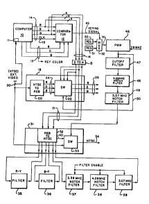
Rsferring to Figure 1, a computer 10 is illustrated which may b~ any one of
a plurality of commercially available computers such as the APPIQ 11 computer.
The computer includes a m~mory which is used as a frame buffer. A user may
enler into this frame buffer signals representing an image (overlay image) which is
displayed in conjunction with anothar imagQ. This other image is illustrated as an
NTSC (extQmal) video signal (composite video signal) applied to line 30. Ths
signal on line 30 may be receivcd from a TV broa~casting station, video disk,
video tape, anothsr computQr, or other source of compositQ video signal.
l h~ extemal video signal on line 30 is shown coupled to a circuit 11 within
computer 10. This arcuit provides synchronization signals to determine ths rate
at which data is r~ad from ths frame buffcr onto lines 14. This is the dot clockfr~quency M pr~viously discuss~d in conjunction with Figure 2. This clot clock is
coupl~d to the comparator 12 on lin~ 16 as illustrated in FigurQ 1. - `
~5 GQn~ralb~ for a video overlay, the frame buffer in the computer 10 stores the
ovQrlay imagQ in any color except for ons color referrQd to the as th~ key color.
Th~ It9y color is storQd in all other pixel locations. The key color is coupl~d to th~
13276~8
conlparator 12 by lines 13 als illustrated in Figur~ 1. On a pixe~by-pixel basis, the
key color is compared to the contents of th~ ~rame buffer as the color data is read
from the frame buffer. When the key color is not the same color as contained in the
frame buffer, the overlay is display~d and th~ comparator 12 provides a k~ying
6 signal on line 45. This is a common prior art technique. (In some cases, indices to
colors in a color lookup 1able are stored in the ~rame buffer.)
The comparison shown in Figure 1 within comparator 12 is a digital
comparison. The digital RGB signals (both th~ signals on line 14 and th3 key
color) can be com/erted to analog form and the comparison done by comparing
10 two analog signals. As illustrated the digital signals on lines 14 (four bits for each
color) are converled to analog form (one analog signal for red, one ~or green and
one for blue) by convcrters 15 and thsn coupled to switch 22 and conn3ctor 32.
This conversion, howev~r, is not don~ ~or the comparison function.
The keying signal on line 45 controls a pulse width modulated signal
1~ generated by an ordinary gating means ~modulator 46) so as to provide blending
(fading) between the ov~rlay image and th~ external vid~o image~ Registers 50
and 51, writabl~ by the computer 10, each store a 4 bit code that indicates thc
level of blending for each state, 0 or 1, of kcying signal 45~ A multiplex~r 52,controlled by the keying signal 45, selects between ths output codes of registsrs
20 50 and 51 and couples tho selectcd cod~ through lines 70 to the modulator 46. A
signal of approximately 28MHz is couplQd to tho modulator 46 as the pulse width
clock and the modulator 46 generates a pulsQ width modulated signal ot a duty
cycle specified by th~ code on lines 70. Th~ presently preferred embodiment
supports pulse width modulation duty cycles of 0~/100%, læ5~o/87.5%, :
25 25Yo/75%, 50%l50%, 75%l25%, 87.5%/12.5%, and 100%/0%.
The pulso width modulated signal generated by modulator 46 is tho
swTtching signal used by the present invcntion to select between the ov~rlay
. .
. . . . . . .
1327648
image and the extemal video image. Since the pulse width modulation can
provide a rapid switching between the two images, it is possible to creata the
illusion of a weighted blending (fading) between the two images. For example, itthe duty cycle of the pulse width modulation is 25%/75%, then a blending of 25%
5 of one image and 75% of the other image is achieved. The two fade registers 50and 5t provide for a different blend weighting for each state of the keying signal.
For simple keying with ~lading turned of~ the code in fade register 50 is set to100%/0% blending and the code in fade register 51 is set to 0/J100% blending.
To reduce aliasing of th~ pulse width modulation of modulator 46 with image
t 0 patterns in the overlay image, the pulse width modulation phase can be inverted
each video field, and inverted again each video frame. This causes the overlay
image and external video imags keying pattern to alternate by video line and by
video frame for an enhanced blending eff~ct.
The keying signal is coupled to switch 22 and, after being filtered by a cutoff
15 filter 47, is coupled to filters 48 and 49~ The filters 48 and 4g have the center
frequenciesoftheirnotcheslocatedat 4.09M~z and 3.07MHz a~ taught by the
present invention and described in coniunction with Figures 2 and 3. The filtering
of the keyin~ signal has been found to reduce artifacts~
In accordance with the present inv~ntion, two merging switches are used to
20 mQrgs the extarnal video signal on line 30 with the overlay signal. In a first circuit
18, the extemal video signal is converted from its NTSC format (or other composite
forrnat) to RGB signals by a converter 20. The RGB signals resulting from this
conversion (three analog signals) are connected to a first switch 22 via lines 24.
Switch 22 selects between the ou1put of the converter 20 and the RGB signals
25 representing the video overlay from the computer 10. The outputs of switch 22 are
merged RGB analog signals on lines 26. That is, the signals on line 26 contain,
11 ~` '""'
.
1327648
fro"l a viewing standpoint, th~ external video image overlayed with the overlay
image ~rom the computer 10~
Gircuit 18 may be a commercially available part, such as Motorola
TDA3301. For this commercial part the switch 22 selects either the signals on
lines 14 or 24 (not a blend o~ both) and lor this reason the output of a pulse width
modulator 46 is used to provide the ~ading.
A second circuit 31 includes a converter 32 which converts the RGB
signals on lines 72 to an NTSC signal on line 40. The switch 33 selects between
the composite signals on lines 30 and 40. The merged output composits signal on
1 0 line 34 represents the same image as the ima~e represented by the signals on line
26.
The circuit 32 may be a commQrcially available arcuit such as th~ Motorola
MC1378. For this àrcuit, the switch 33 is not ~discrete~, that is, depQnding on the
bvel of the control signal to ths switch, both composite input signals can be
1 5 simultaneously selected, thsreby providing blending between the signals. For this
reason, the keying signal from the pulse width modulator 46 i~ tirst coupl~d to a
cutoff filter 47 which sffectively convsrts the pulse width modulated signal to an
analog control signal for thQ switch 33. This keying signal is then coupled to filters
48 and 49 as discussed in conjunction with Figure 2 and 3. The output of the filter
20 4g provides a control signal for the switch 33~
The drcuit of Figure 1 provides both an RGB and composite video output
signals (lines 26 and 34, rsspectiveh"). Importantly, it should be noted that noportion of the signals on lines 26 have been twice converted and the same is true
~or th~ NTSC signal on line 34. In the prior art, the double merging provided by25 switchQs 22 and 33 was not employed
The convertsr 32 provides temlinals to which filters may be coupl~d. The
finers 35, 36 and 37 are ordinary flltels which are coupled to the R-Y, B-Y and Y
. . - . ~ . ; . ~ . . .: . . .
1327648
terminals. Additionally, as dilscussed previously, with the present invention,
additional notch filters 38 ancl 39 are used to filter the luminance component of the
compositesignal. ThesefiltersprovidenotcheSCenteredat 4.09 and 3.07MHz for
an NTSC signal where the dot Glock frequency is cqual to 12.272MHz.
For some video signals artifacts may not appear because of the very nature
of the image/colors defined by the signal (e.g., black and white signal). In these
cases, it may be desirable to disable particularly filters 37, 38 and 39 to maximize
bandwidth. A filter enable signal is shown coupled to these filters to allow, for
example, the manual selection/deselection of the filters.
Thus, an apparatus has been described which provides improved
conversion of a computer generated RGB signal to a composite signal. In the
presently preferred embodiment, this improved conversion is used as part of a
video overlay apparatus which has both an NTSC and RGB outputs.
13
, :
- : . . - . . . ... ~-, , .. , ,.. ,. ,.. ~...... . . . .