Note: Descriptions are shown in the official language in which they were submitted.
1328026 72434-98 `
APPARATUS AND METHOD FOR ENHANCED VIRTUAL
TO REAL ADDRESS TRANSLATION FOR ACCESSING .-
A CACHE MEMORY UNIT
BACKGROUND OF THE INVENTION `~
1. Field of the Invention
This invention relates generally to the cache memory
units associated with central processing units of data processing
systems and, more particularly, to the accessing of the cache
memory unit by the central processing unit.
Brief De~cription of the Drawings
. . : .
Figure 1 is a block diagram of a typical data
processing system capable of using the present invention.
Figure 2 is a flow diagram illustrating the virtual
to real address translation for use with a cache memory unit ~ `
according to the prior art.
Figure 3 is a flow diagram illustrating the virtual
to real address translation for use with a cache memory unit
according to the present invention. `
2. Description of the Related Art
In the modern data processing system, each signal
group has an address associated therewith. The address is used `
for identifying a location in the data processing system main `
memory unit and can act as an identifier of the signal group
itself. In practice, a signal group can have at least two
addresses (i.e., identifiers~,, a virtual address, the address by
which the central processing unit identifies the signal group,
and a real address, the address which identifies a particular
~ .
,.
1328026 72434-98
location in the data processing system main memory unit.
The modern data processing system typically includes
a cache memory unit associated with the
.' . .
2 ~328026
; central processing unit. The cache memory unit acts
as a buffer mechanism between the relatively slow
retrieval of signal groups ~rom the main memory unit
and the immediacy requirement o~ the central
processing unit for requested signal groups. The
cache memory unit stores signal groups that have a
high probability of requirement by the central
processing unit. The location in which a signal
group is stored in a cache memory unit is related to
the real address as will be clear to those familiar
with the related art.
Referring to Fig. 1, a typical data processing
system is illustrated. The main memory unit 13
stores the data signal groups required by the central
processing unit 14 to execute the desired procedures.
Signal groups with a high probability for requirement
by the central processing unit 11 from the main
memory unit 13 or a user unit 15 are trans~erred
through a system interface unit 11 to the cache
memory unit 12. In some data processing system
architectures, the signal group~ are transferred over
a system ~us, thereby requiring an interface urlit for
each component interacting with the system bus. The
signal group~ are stored in the cache memory unit 12
until requested by central processing unit 14. To
retrieve the correct signal group, address
translation apparatus 141 converts the virtual
1328026
--3--
address, used by the central processing unit 14 to
identify the signal group, to the real address used
for that signal group by the remainder of the data
processing system to identify the signal group. The
address translation apparatus is typically
initialized and maintained by the data processing
system operating system. After processing in the
central processing unit 14, the signal group is
returned to the cache memory unit 12 at an address
determined by the address translation apparatus and
consequently transferred to the user unit 15 or main
memory unit 13, as specified by the program. It will
be clear to those familiar with data processing
systems that the ~oregoing description is a synopsis,
data processing systems being more complicated and
having alternate embodiments di~fering ~rom the
roregoing description. This description is provided
as a ~ontext for understanding the present invention.
Referring next to Fig. 2, the process o~
accessing a selected signal group in a cache memory
unit 25 by the central processing unit 14 according
to the p~ior art is illustrated. A virtual address
21 of a signal group to be accessed is provided by
the central procassing unit, typically in a register
23. The virtual address includes at least two
portions, a WORD portion 21A consisting o~ n logic
bit positions and a VIRTUAL PAGE NUMBER portion 21B
-4- 132802~ -
consisting of m logic bit positions. To determine
the real address stored in register 23, the WORD
. . portion 21A o~ the virtual address 21 is used, .
unchanged, as the WORD portion 23A, while the
VIRTUAL PAGE NUMBER portion 21B of the virtual
address is applied to an associative memory 22. The
signal group accessed in the associative memory 22 as
a result of the application o~ the VIRTUAL PAGE
NUMBER portion 21B thereto becomes the m logic bits
of the REAL PAGE NUMBER portion 23B stored in
register 23. This address translation $s typically
implemented to be completed in one clock cycle To.
The real address stored in register 23 is now used to
access the contents of the cache memory unit 25. To
the n bit positions of the WORD portion 23A of the
real address are added b bits ~rom the REAL PAGE
NUMBER portion 23B to ~orm a LOCATION address and the
LOCATION address is applied to address in terminals
of cache directory unit 251 and the address in
terminals o~ cache storage unit 252. At this
location, identi~ied by the LOCATION address, in the
cache storage unit can be, under appropriate
conditions, the signal group which is the signal
group required by the central processing unit. At
this location, identified by the LOCATION address, in
the cache directory unit is stored the signal group
corresponding to the logic signals stored in the m-b
\
:- 13~8026
bit positions of the REAL PAGE NUMBER portion 23B,
generally referred to as the COMPARISON address, of
the real address of the signal group stored in the
addressed location of the cache storage unit. In
other words, the location address and the
(COMPARISON) address signal group stored in the cache
directory unit together form the address of the
signal group stored at the corresponding location in
the cache storage unit. As a result of applying the
LOCATION address to the cache storage unit 252, the
plurality of signal groups, generally referred to as
levels, stored at the addressed location are applied
to multiplexer unit 254. As a result of the
LOCATION address being applied to the cache directory
unit 251, a signal group stored therein is compared
with the remaining m-b signals Or the REAL PAGE
N~MBER portion 23B of the real address 23 in
comparison unit 253. When the comparison results in a
T~UE signal, then the signal group at the LOCATION
address is identified by the real address 23 and a
selected signal group (or level identified by signals
from the comparison unit) is transferred by
multiplexer unit 254 to the central processing unit.
When comparison results in generation of a FALSE
signal, this signal is transmitted to the central
processing unit for appropriate response, typically
retrieval of the identified signal group from the
:
,
.
-6- ~328026 ~:
main memory unit. The cache memory unit access
requires a second system clock cycle To. -
As will be clear to those skilled in the art of
cache memory unit technology, the plurality of signal
groups (or levels) stored at each location in the
cache storage unit is used to reduce the time needed
to retr~eve a signal group from the cache memory
unit. A desirable improvement would be the storage
of a single signal group at each memory location.
In the related art, U.S. Patent 3,979,726; U.S.
Patent 4,264,953 and U.S. Patent 4,669,043 discuss
the use of virtual addresses in combination with
cache memory units, but do not describe techniques
for speeding the translation of virtual addresses to
real addresses. U.S. Patent 4,332,010 describes a
cache memory unit in which the location address is
the WORD ~non-translatable) portion, thereby limiting
the size of the cache memory unit. U.S. Patent
3,723,976s U.S. Patent 4,612,612 and U.S. Patent
4,682,281 contain apparatus responsive to virtual
addresses and apparatus responsive to real addresses
for accessing cache memory signal groups, thereby
greatly expanding the apparatus and the complexity of
the data processing system.
A need has therefore been felt for apparatus and
an associated method expediting the acces~ of signal
groups stored in a cache memory unit with real
-7- 13280~6
addresses in response to virtual address access
requests from the central processing unit. ~ -
FEATURES OF THE INVENTION
It is an object of the present invention to
provide an improved data processing system.
It is a feature of the present invention to
provide an improved technique for accessing a cache
memory unit of a data processing system.
It is another feature of the present invention
to expedite access to signal groups identified by a
real address and stored in a cache memory unit when a
signal group identi~ied by a virtual address is
reguired by a central processlng unit.
It is yet another fQature of the present
invention to provide an improved virtual to real
address translation $or use with a cache memory unit.
It is a still further feature of the present
invention to provide a cache memory unit in which a
single signal group is stored in each cache storage
unit location.
It is a ~ore particular feature of the present
invention to use a portion o~ the virtual address to
determine a trial address for the cache directory
unit and to determine by the time that the contents
o~ the cache directory unit are available whether the
trial address is correct.
':
1328026
-8-
SUMMARY OF THE INVENTION
The aforementioned and other features are
accomplished, according to the present invention, by
providing a small associative memory, responsive to
at least a portion of the virtual address, that
stores trial bits of the cache memory unit location
address to be used until the translation of the
virtual page number to the real page number can
provide the correct bits o~ the cache memory location
address. The stored bits are used, in conjunction
with the location address logic bits that do not
require translation, to access a location in the
cache directory unit prior to the development of the
real address required in such an access. When the
contents Or the cache directory unit are avallable
for comparison, the translation ~rom the virtual
address i5 complete. ~he translated portion o~ the
real address that isi to be used in the comparison
with the signal group from the cache directory unit
20 i8 available and the comparison can be per~ormed when
the stored bits used in the cache memory unit
location address are the same as the translated bits.
When the trial and the translated bits of the
~; location address are the same and the comparison o~
the real address translated logic signals is the same
as the corresponding address logic signals stored in
the cache directory unit, then the contents of the
., .
9 ~328026
72434-98
cache storage unit are the desired signal group. When the stored
and translated location address logic signals are not identical,
then the real address, available from translation procedure, is
applied to the cache memory unit in mode of operation similar to
the typical cache memory unit operation.
In accordance with the present invention, there is
provided a cache memory unit for holding data units to be supplied
when data units are requested from the main memory of a data
processing system; said system including a processor of said :
system, when requesting a data unit stored in sai.d main memory,
supplying a virtual address of the main memory location in which
said data unit is considered to be stored, said virtual address
including a first portion (n bits, bits 0 to n-l), a second
portion (b bits, bits n to n + b-l) and a third portion (m-b bits,
bits n + b to m + n-l); wherein said cache unit includes an
associative memory, an addressable data store and an addressable
directory, said associative memory for translating said second
and third virtual address portions to second and third real
address portions having the same number of bits as the corres-
ponding virtual address second and third portions, the first
address portions of said virtual and real addresses being the
same, said data store and directory being addressed by the :~.:.-
combination of said first and second real address portions, said
directory for holding a third real address portion in each
storage location thereof, said data store for holding a data
unit in each storage location thereof which data unit is
considered to be a copy of a data unit stored in the main memory
:'. .
,:,.
A -
, . . . . . .. . . . . ..
-9a- 1 3 2 8 02 6
72434-98
. location whose address is the combination of the address of said
,~: data store location and the third address portion held in the
', corresponding directory location; said cache memory unit being
characterized by: a storage unit for holding a second real
v. address portion in each storage location thereof and for deliver-
ing the contents of one of said storage locations upon receipt
~x of an input address thereby; means for applying as an input
address to said storage unit at least selected bits of the second
and third virtual address portions received by said cache memory
unit; means for applying as a trial address to said directory
the second real address portion delivered by said storage unit
and the first virtual address portion received by said cache
memory unit; and a comparator for comparing the second real
address portion delivered by said storage unit with the second
real address portion generated by said associative memory;
whereupon, if said comparator detects equallty between the two
second real address portions compared thereby, said comparator
delivers a first signal to cause said cache memory unit to proceed
using the third real address portion delivered by said directory :
in response to the trial address applied to said directory.
In accordance with another aspect of the invention,
there is provided a method for retrieving a signal group in a
cache memory unit stored at a location determined by an
associated real address by a central processing unit identifying
said signal group by a virtual address, said method comprising
the steps of: obtaining a trial address determined from at least :
a portion of said virtual address; applying said trial address to -
~ '.
-9b- 13~8026
72434-98
a cache directory unit to obtain a stored address portion; trans-
lating said virtual address to said real address; comparing said
trial address with a first selected portion of said real address;
when said comparing step is positive, comparing said stored
address portion with a second selected portion of said real
address; and when said comparing step involving said stored
address portion is positive, using a third portion of said real
address to access a cache storage unit, thereby retrieving said
signal group.
In accordance with a further aspect of the invention,
there is provided a cache memory unit for holding data units to
be supplied when data units are requested from the main memory
of a data processing system; said system including a processor of
said system which, when requesting a data unit stored in said .:
main memory, supplies a virtual address of the main memory
location in which said data unit is considered to be stored; :.
wherein said cache unit includes an associative memory, an :
addressable data store and an addressable directory, said
associative memory for translating said virtual address to a
corresponding real address, said data store and directory being
addressed by a portion of said real address, said directory for
holding another real address portion in each storage location - :
thereof, said data store for holding a data unit in each storage - .
location thereof which data unit is considered to be a copy of a
data unit stored in the main memory location whose address is the .. :
combination of the address of said data store location and the
real address portion held in the corresponding directory location; -
'., ' :
. .~
-gc- 13280~6
72434-98
said cache memory unit being characterized by: a storage unit
for holding a real address part in each storage location thereof
and for delivering the contents of one of said storage
locations upon receipt of an input address thereby; means for
applying as an input address to said storage unit at least
selected bits of the virtual address received by said cache
memory unit; means for applying as a trial address to said
directory at least the real address part delivered by said storage
unit; and a comparator for comparing the real address part
delivered by said storage unit with the corresponding real
address part generated by said associative memory; whereupon, if
said comparator detects equality between the two real address
parts compared thereby, said comparator delivers a first signal
to cause said cache memory unit to proceed using the address
portion delivered by said directory in response to the trial
address applied to said directory.
These and other features of the invention will be
understood upon reading of the following description along with
the drawings.
DESCRIPTION OF THE PREFERRED EMBODIMENT
1. Detailed Description of the Figures
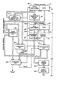
Referring now to Fig. 3, the functional block diagram
of the apparatus of the present invention is illustrated. Fig. 3
is a redrawing of Fig. 2 with the additional apparatus of the
present invention and with the components of the cache memory
unit arranged to emphasize the signal flow. The central processing
A :
1328026
--10--
unit provides a VIRTUAL PAGE NUMBER PORTION 2 lB
address in register 21 to the address translation
apparatus represented by associative memory unit 22.
Simultaneously, the VIRTUAL PAGE NUMBER 21B or a
portion thereof is applied to small associative
memory unit 31. The small associative memory 31,
responsive to at least a portion of the virtual
address, has a relatively small number of directly
j accessed storage locations provident relatively small
signal groups, thereby permitting identification o~
an associated signal group without significant delay.
The si~nal group developed by the small associatlve
memory unit 31 contains a trial signal group to
complete, along with th~ WORD portion 21A, a TRIAL
LOCATION ADDRESS. The TRIAL LOCATION ADDRESS is
applied to address in terminals of the cache
directory unit 251. The contents of the cache
directory unit 251 determined by the TRIAL LOCATION
ADDRESS are stored in comparison unit 253.
Simultaneously, the application of the VIRTUAL PAGE
NUMBER 21B to the associative memory unit 22 results
in the storage of the REAL PAGE NUMBER 23B in
appropriate locations of register 23. The portion of
the REAL PAGE NUMBER 23B that forms part of the
LOCATION ADDRESS 24A is applied to comparison unit 32
and compared with the signal group from the small
associative memory unit 31. A positive comparison
1328~26
from comparison unit indicates that the correct
location in the cache directory unit 251 has been
addressed by the TRIAL LOCATION ADDRESS. The portion
of the REAL PAGE NUMBER 23B that is the COMPARISON
ADDRESS is applied to the comparison unit 253 and
compared with the contents from the cache directory
unit, the comparison unit 253 being enabled by TRUE
signal (or positive comparison from the comparison
unit 32). When the two quantities applied to the
enabled comparison unit 253 are not the same, then a
FALSE signal is generated and applied to the central
processing unit. The FALSE signal from comparison
unit 253 indicates that the signal group required by
the data processing unit is not stored in the cache
storage unit 252 and the required signal group must
be retrieved from the main memory unit. When the
enabled comparison unit 253 issues a TRUE signal,
then multiplexer unit 36, which has th~ LOCATION
ADDRESS applied thereto has the LOCATION ADDRESS
applied to the address in terminals of the cache
storage unit 252. The result of the application of
the ~OCATION ADDRESS is to apply the required signal
group to tho output r~gistsr 354. Th~ cache storage
locations contain only one signal group and,
2S therefore, an output multiplexer is not required.
When the comparison unit 32 provides a FALSE
~ignal, indicating that the TRIAL LOCATION ADDRESS is
13~8026
-12-
not the correct LOCATION ADDRESS, as a result of the
comparison operation, the FALSE signal is applied to
;multiplexer unit 36. By the time of the generation
of the FALSE signal from comparison unit 32, the
correct LOCATION ADDRESS 24A is available in register
23. As a result of the application of the FALSE
i'signal to multiplexer unit 36, the LOCATION ADDRESS
i~24A is applied to address in terminals of the cache
directory unit 251. The location addressed as a
.10 consequence of the application o~ the LOCATION
ADDRESS are entered in comparison unit 253 and
compared with the COMPARISON ADDRESS 24B. As a
result of this comparison, a FALSE signal will
indicate to the central processing unit that the
required data signal group is not stored in the cache
memory unit 25 while a T~UE signal causes the
LOCATION ADDRESS to be applied (~rom multiplexer unit
36) to the address in terminals of cache storage unit
252 and the required signal group to be applied to
output register 254.
A second FALSE signal is shown originating from
the comparison unit 32. The signal is used to freeze
the contents of the data signal group in register 21
and register 23 in order that a second access of the
cache directory unit can be accomplished without
interference from the next virtual address ~ignal
group. When this FALSE signal is generated, the
,'
1328026
-13-
small associative memory 32 is updated by storing the
portion of the REAL PAGE NUMBER 23B that is included
in the LOCATION ADDRESS at a location determined by
the VIRTUAL PAGE NUMBER.
The operation of the cache directory and the
operation of the virtual to real address translation,
which operations are performed in parallel, can be
implemented in one system clock cycle To~ while the
withdrawal o~ the required signal group can be
performed in the next consecutive cycle To.
2. Operation of the Preferred Embodiment
The efectiveness o~ the present invention
relies on the ~act that a so~tware program will
typically reference signal groups in only a few
memory data pages ~or extended portions of the
program. As a result, only a limited number REAL
PAGE NUMBER 23A signal groups will be required.
There~ore, a small associative cache memory unit (31)
aan accommodate REAL PAGE NUMBER portions of the
memory data pages currently being accessed by the
central processing unit. (It will be clear that the
entire VIRTUAL PAGE NUMBER 21B need not be applied to
small associative memory unit 31 and that a portion
thereo~ can be su~icient). Thus, the small
associative memory unit permits an assumption to be
made concerning the results o~ the virtual to real
address translation. The contents o~ the small
-14- 1328026
associative storage unit 31 can be determined, in the
preferred embodiment, by entering the b signal bits
from the REAL PAGE NUMBER into the location addressed
by the VIRTUAL PAGE NUMBER. To the extent that the
5 central processing unit continues to reference the -
same or relatively few virtual page numbers for
extended periods of a procedure, the small
associative memory will provide an accurate TRIAL
ADDRESS, thereby enhancing performance.
The invention uses two system clock cycles,
i.e., 2-To, similar to the prior art implementation
illustrated in Fig. 2. However, the cache memory
unit 25 is pipelined such that a wrong assumption
concerning the LOCATION ADDRESS portion derived from
the VIRTUAL PAGE NUMBER (i.e., via the small
associative memory unit 31) results in the cache
memory unit retrieval cycle while a series of correct
assumptions permits a signal group to be retrieved
from the cache memory unit every system clock cycle
To.
The disclosed apparatus has the further
advantage that the implementing apparatus is
rel~tively simple and can be conveniently included
with cache memory unit. In addition, the appropriate
level signal group of the plurality of levels of
signal groups typically associated with each cache
storage level address can be selected so that only
: '
,.
1328026
-15-
the required signal group need be transferred to the
central processing unit.
The foregoing description is included to
,,,:
illustrate the operation of the preferred embodiment
and is not meant to limit the scope of the invention.
- The scope of the invention is to be limited only by
, the following claims. From the foregoing
description, many variations will be apparent to
those skilled in the art that would yet be
enco~passed by the spir1t and scope o~ the invention.