Language selection

Search

Patent 1328183 Summary

Third-party information liability

Some of the information on this Web page has been provided by external sources. The Government of Canada is not responsible for the accuracy, reliability or currency of the information supplied by external sources. Users wishing to rely upon this information should consult directly with the source of the information. Content provided by external sources is not subject to official languages, privacy and accessibility requirements.

Claims and Abstract availability

Any discrepancies in the text and image of the Claims and Abstract are due to differing posting times. Text of the Claims and Abstract are posted:

  • At the time the application is open to public inspection;
  • At the time of issue of the patent (grant).
(12) Patent: (11) CA 1328183
(21) Application Number: 609006
(54) English Title: OPTICAL MODULE
(54) French Title: MODULE OPTIQUE
Status: Deemed expired
Bibliographic Data
(52) Canadian Patent Classification (CPC):
  • 345/62
  • 88/97.7
(51) International Patent Classification (IPC):
  • G02B 6/42 (2006.01)
  • H01L 31/0203 (2006.01)
(72) Inventors :
  • SHIGA, NOBUO (Japan)
(73) Owners :
  • SUMITOMO ELECTRIC INDUSTRIES, LTD. (Not Available)
(71) Applicants :
(74) Agent: MARKS & CLERK
(74) Associate agent:
(45) Issued: 1994-04-05
(22) Filed Date: 1989-08-22
Availability of licence: N/A
(25) Language of filing: English

Patent Cooperation Treaty (PCT): No

(30) Application Priority Data:
Application No. Country/Territory Date
210119/1988 Japan 1988-08-24

Abstracts

English Abstract


Abstract of the Disclosure
In an optical module with a substrate having an
optical unit mounted thereon being provided on a bottom
of a package and having the optical unit optically
coupled with an end of an optical fiber extending into
the package, a chip carrier including the optical unit
is die-bonded to a conductive land formed on the
substrate, and a recess is formed at an area of the
bottom of the package which faces the land. Thus, a
capacitance of a parallel-plate capacitor formed by the
land and the bottom of the package, which prevents a
high speed operation, is rendered negligibly small.


Claims

Note: Claims are shown in the official language in which they were submitted.


THE EMBODIMENTS OF THE INVENTION IN WHICH AN EXCLUSIVE
PROPERTY OR PRIVILEGE IS CLAIMED ARE DEFINED AS FOLLOWS:
1. An optical module coupling device comprising:
a metallic package; a substrate made of insulative
material and provided on the bottom of said package, said
substrate having a conductive land on one side thereof and
an area in opposition to said land on the opposite side
thereof; and a chip carrier mounted on said substrate and
having an optical unit to be optically coupled with an end
of an optical fiber extending into said package, said area
of said substrate being spaced from said bottom of said
package.

2. An optical module coupling device according to claim 1,
wherein said optical unit comprises a photo-detecting
element.

3. An optical module coupling device according to claim 1,
wherein said optical unit comprises a light emitting device.

4. An optical module coupling device comprising:
a metallic package; a substrate made of insulative
material and provided on the bottom of said package, said
substrate having a conductive land on one side thereof and
an area in opposition to said land on the opposite side
thereof; and a chip carrier mounted on said substrate and
having an optical unit to be optically coupled with an end
of an optical fiber extending into said package, said bottom
of said package having a recess located in opposition to
said area.

5. An optical module coupling device according to claim 4,
wherein said optical unit comprises a photo-detecting
element.


6. An optical module coupling device according to claim 4,
wherein said optical unit comprises a light emitting
element.

7. An optical module coupling device comprising:
a metallic package; a substrate provided on the bottom of
said package, said substrate having a conductive land
thereon; and a chip carrier mounted on said substrate and
having an optical unit to be optically coupled with an end
of an optical fiber extending into said package; said
substrate being spaced from said bottom of said package at
an area opposite to said land, and said device including a
parallel plate capacitor formed by said land and said bottom
of said package.

8. An optical module coupling device according to claim 7,
wherein said substrate is made of insulative material.

9. An optical module coupling device comprising:
metallic package; a substrate made of insulative material
and provided on the bottom of said package, said substrate
having a conductive land thereon; and a chip carrier mounted
on said substrate and having an optical unit to be optically
coupled with an end of an optical fiber extending into said
package; said bottom of said package having a recess at an
area which is opposite to said land, and said device
including a parallel plate capacitor formed by said land and
said bottom of said package.

10. An optical module coupling device according to claim 9,
wherein said chip carrier comprises insulative material and
conductive terminals formed on said insulative material.


Description

Note: Descriptions are shown in the official language in which they were submitted.


~32~3

The present invention relates to an optical module for
use with an optical communication ~ys~em such as data link or
an optical LAN which uses light as an in~ormation
transmission medium.


In ~ known optical module, a semiconductor laser or a
light emitting dlode, whi~h is a light emitting element, or a
PIN photo-diode which is a light de~ecting element i~ mounted
as an optical unit, which is optically couple~ with an
optical fiber in a package. However, a re~ponse ~requency
band of the known optical module i~ not sufficiently high.


The present invention provides an optical module with a
$ub~trate having an optical unit mounted thereon being
provided at a bottom of a package and having the optical unit
optically coupled with an end of an optical fiber extending
into the package, a chip carrier including the optical unit
being die-bonded to a c~nductive land formed on the substrate
and a recess being formed at an area of ~he bottom of the
package which face th~ land.


~;~ i


.. . . .
. .
.
. .
.
:: .

t 32~183


The present invention will become more Pully understood
from the detailed desaription given herein~low and the
accompanying drawings in whlch:


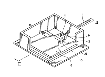
FIG. 1 is a perspective view showing a main part of an
optical module in accordanGe with one embodiment of the
present invention,


FIG. 2 is a ~ectional view taken along a line II-II of
FIG. 1,


FI~. 3 is a perspective view illustrating a manner of
die-bonding of a chip carrier 2 to a hybrid IC substrate 6,
and


FI~. 4 is a circuit diagram of a light receiver which
use6 a PIN photo-diode.


As shown in Fig.1 and 2, a hybrid IC substrate 6 made of
ceramics is mounted on an inner bottom of a package 8 made of
metal. A chip carrier 2 is mounted on the hybrid IC
substrate 6.


~ 2


.. .,. ~, ,: . . ..
- ~ ~ '1"- ' . . .
- ~ . .
,. ~.. ~ .. ,

132~18~3

As shown in Fig. 3, the chip carrier 2 is o~
parallelepiped and ~ade o~ ceramics. A PIN photo-diode 3 is
mounted on a front plane of the chip carrier 2. Two
terminals 5 which are to be connected to an anode and a
cathode of th~ PIN photo-diode 3 on the chip carrier 2 are
~ormed to extend from the front plane to a bottom plane.
Those termical~ 5 are formed by ~etallizing selected ~ur~a¢e
area~ of the chip carrier 2. On the other hand, two
conductive lands 7 which serve as electrode~ are Pormed on a
sur~ace o~ the hybrid IC ~ub~trate 6. The terminals 5 of the
chip carrier 2 are die-bonded to the lands 7. The land 7
are designed to have wider areas than the terminals 5
assuming possible misalignment in mounting the chip carrier
2. With present technique, the area o~ the land 7 is in the
order of lmm X 2mm at minimum.


.
The PIN photo-diode 3 mounted on the chip carri~r 2
faces a leading end plane of an optical fib~r 1 in a


c ~

~; .
,

1 ~2~8~
1 package 8. The leading end of the optical fiber 1 is
inserted into the package 8 through an opening formed on
a side wall of the package 8. A cover of the optical
fiber 1 is striped off at the leading end thereof so
that a glass fiber is exposed. The exposed area is
metal-plated except for the leading end plane. The
metal-plated area la is positioned on a fixed member 9
mounted on the bottom of the package 8 and fixed ~hereto

by soldering. The metal-plated area la of the optical
fiber 1 is positioned such that a light emitted from the

leading end plane of the optical fiber 1 is sufficiently
directed to a photo-sensing area of the PIN photo-diode
3. In this manner, the optical fiber 1 and the PIN
photo-diode 3 are optically coupled.
A recess 10 is formed at the inner bottom of the
package 8. The recess 10 is formed at a postion which
faces the lands 7 with the intervention of the hybrid IC
substrate 6 when the hybrid IC substrate 6 is mounted in

the package 8. Thus, the lands 7 and the bottom of the
package 8 are separated from each other by a space. The

recess 10 serves to render a capacitance of a parallel-
plate capacitor, which is essentially formed by t.he
lands 7 and the bottom of the package 8, negligibly
small.
The parallel-plate capacitor which is essentially
formed by the lands 7 and the bottom of the package 8 is
now explained. Fig. 4 shows an embodiment of a light


~ ,

~328183
1 receiver which uses the PIN photo-diode 3. The parallel-
plate capacitor formed by the lands 7 and the bottom of
the package 8 function as an input capacitance Cpal o~
an amplifier 12. A response frequency band of the light
receiver is determined by a time constant T Which is
determined by a resistance Rin of an input resistor 11,
a junction capacitance Cpd of the PIN photo-diode 3 and
the input capacitance Cpal. As the time constant T

increases, amount of information per unit time
decreases. The time constant T is given by

T=(Cpd+Cpal)-Rin
The junction capacitance Cpd of the PIN photo-diode 3
used for high speed optical communication is very small,
usually in the order of 0.3 ~ 0.4 pF. Accordingly, the
affect of the input capacitance Cpal to the time
constant T is very great and it should be as small as -
possible.
If the recess 10 is not formed, the capacitance Cpal

of the parallel-plate capacitor is 0.46 pF assuming that
the area of the land 7 is lmm x 2mm, a dielectric

constant f of the hybrid IC substrate 6 is 9, and a
thickness thereof is 350 ~m, and it is 0.25 pF assuming
that the thickness of the hybrid IC substrate 6 is 650
~m. This capacitance is substantially equal to or
larger than the capacitance of Cpd ~0.3 ~ 0.4 pF). It
is thus seen that the affect to the time constant T is
very great.


'' ' '` ''~:

.
.

~32~1 ~3

In the optical module of the present embodiment, ~ince
the recess 10 is ~ormed in the inner bottom of the package 8,
the capacitance of the parallel-plate capacitor formed by the
lands 7 and the bottom of the package 8 is small enough to
permit neglection o~ the input capacitance Cpal of the
amplifier 12. As a result, the time constant T of the light
receiver ~s reduced and the response frequency band is
increased,


This ~mbodiment is a receiving optic~l module which uses
the PIN photo-diode ~ a the optical unit which is optically
coupled to the optical fiber 1. The same problem is
encountered in a transmitting optical module which uses a
light emitting element such as LED or loser diode as the
optical unit, and the present invention is al~o applicable to
such a transmitting optical module.


, , ,

Representative Drawing
A single figure which represents the drawing illustrating the invention.
Administrative Status

For a clearer understanding of the status of the application/patent presented on this page, the site Disclaimer , as well as the definitions for Patent , Administrative Status , Maintenance Fee  and Payment History  should be consulted.

Administrative Status

Title Date
Forecasted Issue Date 1994-04-05
(22) Filed 1989-08-22
(45) Issued 1994-04-05
Deemed Expired 1998-04-06

Abandonment History

There is no abandonment history.

Payment History

Fee Type Anniversary Year Due Date Amount Paid Paid Date
Application Fee $0.00 1989-08-22
Registration of a document - section 124 $0.00 1989-11-22
Maintenance Fee - Patent - Old Act 2 1996-04-05 $100.00 1996-03-18
Owners on Record

Note: Records showing the ownership history in alphabetical order.

Current Owners on Record
SUMITOMO ELECTRIC INDUSTRIES, LTD.
Past Owners on Record
SHIGA, NOBUO
Past Owners that do not appear in the "Owners on Record" listing will appear in other documentation within the application.
Documents

To view selected files, please enter reCAPTCHA code :


To view images, click a link in the Document Description column. To download the documents, select one or more checkboxes in the first column and then click the "Download Selected in PDF format (Zip Archive)" or the "Download Selected as Single PDF" button.

List of published and non-published patent-specific documents on the CPD .

If you have any difficulty accessing content, you can call the Client Service Centre at 1-866-997-1936 or send them an e-mail at CIPO Client Service Centre.


Document
Description 
Date
(yyyy-mm-dd) 
Number of pages   Size of Image (KB) 
Drawings 1994-07-22 4 61
Claims 1994-07-22 2 89
Abstract 1994-07-22 1 19
Cover Page 1994-07-22 1 19
Description 1994-07-22 6 188
Representative Drawing 2002-05-08 1 16
PCT Correspondence 1993-05-27 3 67
Office Letter 1993-07-08 1 53
Prosecution Correspondence 1994-01-05 1 31
Prosecution Correspondence 1993-05-27 4 107
Examiner Requisition 1992-11-27 2 91
Prosecution Correspondence 1992-09-30 4 106
Examiner Requisition 1992-06-01 1 53
Fees 1996-03-18 1 73