Note: Descriptions are shown in the official language in which they were submitted.
13 2 8 3 7 8 F.N. 42862 CAN 9A
STATIC DISSIPATIVE TAPE
Background of the Invention
1. Field of the Invention
This invention relates to a tape product used to
drain static charge from personnel working in munitions and
chemical plants and with sensitive electronic devices in
circuit assembly areas, and in one,aspect to a tape product
which can be applied as a work surface covering, wall
covering, rug or runner in areas where personnel are
working with such devices to restrict damage due to static
electricity.
~2. Description of the Prior Art
Pads and mats for use in draining static charge
from personnel are known and have been designed for use on
work surfaces of various sorts. An example of such
conductive mats is illustrated in U.S. patent No. 4,208,696
assigned to the assignee of this application. This patent
affords an example of a web comprising a semi-conductive
polymeric surface layer, a conductive layer and a
supporting substrate, for example, a resilient foam layer.
This foam layer provides a cushioning when the web is used
as a floor covering. Alternatively, a thin sheet of stiff
plastic or fiberboard could be used in place of the foam,
when the web is used under chairs and especially when used
under chairs over carpeting. When the web was used as a
floor mat, the thickness of the mat with the form caused
, carts moving between wor~ areas to bounce and the
electronic parts contained therein to be jostled about.
Further, soft mats would roll or wrinkle upon movement of a
¦ cart thereover, making the same not particularly desirable
as floor coverings in the work areas.
The present invention provides a static
dissipative covering for floors which does not have a
height sufficient to cause a cart to be impeded in any way
when rolling onto or off the covering. The tape of the
present invention does not roll or wrinkle eliminating
¦ hazardous areas or areas where the
s
. ' :
1328378
2 60557-~750
material carts could be bounced durlng movement on, along, or off
the same.
Another patent relatlng to statlc dlsslpatlve mats ls
U.S. patent No. 4,363,071 whlch discloses a multilayer mat
comprising an upper layer of low conductivlty, ln the order of 10
ohms per square, bonded to a layer of greater conductivlty ln
order of lO ohms per s~uare, and a bottom layer of expanded
polymerlc materlal of relatlvely low conductlvlty, for example, an
expanded verslon of the materlal of the upper layer. A further
fabrlc base may be lamlnated to the bottom layer of the web as
indicated in U.S. patent No. 4,414,260. The mat resulting had an
overall thlckness of 125 mlls ~3.175 mm) whlch has the same
disadvantage of the web of the earlier patented construction when
used as a floor mat.
Further, ln U.S. patent No. 4,219,602, and earller
lssued U.S. patent No. 3,891,786, there ls dlsclosed a sheetlng
materlal comprlslng an electrically conductive coatlng applled to
a non-porous plastlc substrate layer, the uncoated surface of
whlch ls then adhered to a second non-porous plastlc layer by
means of a plastlsol adheslve. In one embodlment of U.S. patent
No. 4,219,602 a relnforclng layer may be dlsposed wlthln the
plastlsol adheslve layer. The fabrlcs produced by the lnventlon
of that patent were found sultable for use as mattress tlcklng,
covers for wheeled stretcher pads, plllows, tractlon bags as well
as other hospltal appllcatlons. The thlckness of the sheetlng ls
sald to comprlse a l/2 to 1 mll conductive layer and preferably a
2 to 4 mll (0.05 to 0.10 mm) non-conductlve layer. Thls U.S.
patent 4,219,602 teaches a thln sheetlng materlal but not a sheet
-
f,
.~ ~
1~28378
3 60557-3750
materlal for controlled dralnage of static charges. The earller
U.S. patent 3,891,786, dlscloses a conductlve sheetlng comprlslng
a polymerlc fllm, whlch ls perforated, lamlnated to a natural or
synthetlc rubber havlng up to 40% carbon black flller. The
resultant product ls conductlve on the surface of the polymerlc
fllm.
U.S. patent No. 4,424,900 dlscloses a lamlnate materlal
~ for use in the manufacture of packages and ls approxlmately 2 mlls
t` ~o 05 mm) thlck comprlslng a polymerlc substrate adhered to an
antl-statlc polyolefln materlal, wlth a conductlve layer of
sputtered metal applled to elther the substrate, havlng a volume
reslstlvlty of at least 10l ohm-cm, or the antl-statlc layer,
~ havlng a surface reslstlvlty between 106 to 1012 ohms per square.
¦ There ls no teachlng here of a tape material for use on a floor
coverlng or that the adheslve layer should be covered by a
removable llner to form a tape and surely such a product would be
, undeslrable as a packaglng materlal.
U.S. patent No. 3,904,929 dlscloses an electro-
dl~charglng sheet prepared by applylng a carbon black-hlgh
. 20 molecular welght resln composltion to a base materlal lncludlng
woven, unwoven and knlt clothes and paper havlng an afflnlty to
the resln composltlons. The base materlal ls porous and the
materlal of thls lnventlon can be used for clothes, carpet, or
wall materlals. A product of thls lnventlon was belleved to have
been sold by Kohkoku Chemlcal Industry Co., Ltd. as "NON-SPARK
TAPE AND SHEBT" and sold as a wrapplng for piplng, whereln at
' least one end of the tape product had an adheslve coatlng to
, adhere the end to the plpe.
~., , ~ -. , , : .. ; . . . :
1328378
4 60557-3750
The prlor art references have thus provlded teachlngs of
i varlous compositlons of sheets, webs, matsl etc. servlng to
dlsslpate statlc charges whlch might bulld ln the varlous areas.
The need also for materials on the floor have been known, but the
need for a materlal capable of dlscharglng the statlc charges and
yet not dlsrupt the normal flow of people and materlal carts has
not been taught or recognlzed ln the art. Therefore lt ls an
' ob~ect of the present lnventlon to provlde a tape ln sultable
j wldths to use as rugs or runners ln work areas or as floor
~ 10 coverlngs ln assembly areas to provlde a statlc dlsslpatlve
'A surface. The materlals can also be used as wall and work surface
coverlngs.
SUMMARY OF THE INVENTION
The present lnventlon provldes an lmprovement ln statlc
dlsslpatlve tapes and in tape llke materlals that can be used as
rugs or runners, coverlngs for work surfaces and wall coverlngs ln
areas where protectlon agalnst damage caused by statlc electriclty
ls deslred.
More speclflcally, the present lnventlon provldes a
thln, tough, flexlble, durable, statlc dlsslpatlve tape comprlslng
a composlte of.
a flrst layer of statlc disslpatlve polymerlc material -~
havlng a volume reslstlvlty of between 106 to 101 ohm-cm;
a layer of conductlve materlal lamlnated to one surface ~-
; of sald flrst layer and havln~ a volume reslstivlty of less than
104 ohm-cm; and
a layer of pressure sensltlve adheslve applled to the
surface of the conductlve materlal opposlte sald flrst layer for
: "
1328378
4a 60557-3750
applylng sald composlte to a surface,
whlch composlte has a total thlckness less than 1.5 mm
and sufflclent drape to be applled to a radlus of 0.40 mm. The
flrst layer can be smooth or textured and translucent or colored,
to match a decor or for attractlng attentlon. The adheslve ls
preferably coated to a thlckness of 1 to 5 mlls (0.025 to 0.125
mm) and the adheslve ls covered by a removable llner. The
thlckness of the tape lncludlng the thlckness resultlng from the
embosslng of an antl-sllp textured surface to the statlc
disslpative layer ls between 0.015 lnch (0.38 mm) and 0.060 inch
(1.5 mm). The tape of the present lnventlon may also be
perforated to afford ease of applicatlon of wlde wldths of tape.
, From another aspect the lnventlon provldes a method of
j applylng a thln wlde web of statlc dlsslpatlve tape to a surface,
whlch tape comprlses a flrst layer of statlc dlsslpatlve materlal
havlng a volume reslstlvlty of between 10 to lO ohm-cm, a layer
of conductlve meterlal adhered to sald flrst layer and a coatlng
of pressure sensitive adheslve applied to sald conductlve materlal ;-
and covered by a llner comprislng the steps of:
perforating the wlde web,
placlng the web over a sald surface, and
uslng a tool to smooth the surface of the tape on a sald
surface.
~RI~F DESCRIPTION OF THF DRAWING
The present lnventlon wlll be further descrlbed wlth
reference to the accompanylng drawlng whereln;
Flgure 1 ls a fragmentary cross sectlon of a completed
tape structure;
.:
: . - i .. . .. ... :
1328378
4b 60557-3750
Flgure 2 ls a fragmentary detall cross sectlon of a tape
structure of the present lnventlon to lllustrate the surface of
one of the layers; and
Flgure 3 ls a schematlc plan vlew of the tape of the
present lnventlon when spplled.
.
~,
1328378
-5-
Description of the Preferred Embodiment
The present invention relates to a tape
construction for use in areas where it is desirable to
restrict the rapid discharge of any static charge that may
have built up on people or equipment accessing the area.
The invention provides an improved tape construction that
can be positioned on the floor, in a hallway, an aisle,
asslembly areà or door way, on walls, work or storage areas
or surfaces. The tape once in place will serve to
dissipate the static charge built up on an individual
coming in contact with the tape to restrict such charge
from being suddenly drained to and damaging a static
sensitive electronic device. The sudden spark discharge of
static electricity is also uncomfortable to the individual
and presents an explosive hazard in the presence of some
chemicals, explosive dusts and munitions.
The tape of the present invention is generally
designated by the reference numeral 5 and comprises a first
layer of a static dissipative material 6 and a second layer
8, in contact with the first, of a conducti,ve material. A
third layer coated onto the surface of the conductive layer
8 opposite the dissipative layer is a layer of pressure
sensitive adhesive material 10 coated uniformly over the
surface of the conductive layer 8. A removable liner
material
12 ~ay be positioned in contact with the exposed surface of
the adhesive coating 10.
The first layer 6 comprises a durable tough
flexible thermoplastic polymeric material with a volume
resistivity of between 106 and 1012 ohm-cm. The layer 6 is
formed on one æurface with a smooth easily cleaned surface,
forming a better writing surface, or with a patterned,
matte or embossed surface, see Figure 2, providing a non-
slip surface and improve the appearance of the tape. If
opaque the tape may be colored to match a given decor or
colored to accent or attract attention to an area. The
first layer i6 formed as a film having an initial thickness
of O.OOS to 0.0~5 inch ~0.127 to
: -
'.~ ' ' ' ' ' ' ~ ' ' . . . ', ' " , "' ' ' " .
1328378
-6-
0.38 mm) and is subsequently coated by an extrusion process
with material forming the conductive layer 8. The
polymeric material preferably is a static dissipative
polyvinyl chloride film which is opaque, translucent or
transparent. A preferred example of a suitably tough,
flexible, durable polymeric material is as follows:
MATERIAL PARTS DESCRIPTION _
Resin 100 PVC Resin VC-106-PM
Additives 5 Antimony Trioxide
3 Stabilizer PG Dyphos
.5 Hoechst OP Wax
Powder
.4 UV Absorber W9
Cyasorb 7.3
` Varstat-10
MATERIAL PARTS
DESCRIPTION I -
Plasticizers 45 9780 Plastolein
Santicizer 711
, 7 Plas-Chek 775
If opaque, the tape is pigmented with an esthetic gray or
brown color, or other color of choice. The surface
texture, as indicated at 14 in Figure 2 is formed by a
texturing roll positioned in advance of the surface coater
app,lying the conductive coating to the film.
The conductive layer 8 comprises a homogenous
layer of polyvinyl chloride material having dispersed
therein quantities of carbon or metal to provide a coating
having a volume resistivity of less~than 104 ohm-cm. The
conductive layer conforms to the adjacent surface of the
first layer 6 and has an opposite smooth surface.
`~ The conductive layer 8 is generally colored by
virtue of the conductive particles dispersed therein. A
preferred material is CV 79-8083-K compound from Teknor
Apex Company of Pawtucket, Rhode Island. Alternatively, it
' could be a think layer of aluminum. If the tape is
transparent the conductive layer may be a conductive non-
woven material formed of metallic fibers dispersed in a
nonmetallic nonwoven matrix.
i
:: : " - ~ - .~ .' ,-: . '
1328378
--7--
The adhesive layer 10 is applied to a smooth
surface of the conductive layer 8. The adhesive layer is
preferably uniform over the entire surface of the
conductive layer and is preferably a pressure sensitive
adhesive having a peel strength to steel of between about
9.8 ounces per inch to 34.6 ounces per inch (110 gram/cm to
390 gram/cm) and preferably 15 ounces per inch (167
grams/cm) when coated uniformly onto the exposed surface of
the conductive layer 8, as measured,by ASTM standard D-
3330. This pressure sensitive adhesive layer 10 permits
ready removal and repositioning of the tape 5 from the
recsptor surface. The thickness of the adhesive layer lO
is about 0.002 inch (0.05 mm). An example of the adhesive
is a compounded material similar in nature to Example 1 of
U.S. Patent No. 3,232,785 assigned to the assignee of this
application. The preferred positionable adhesive and
primer comprises the following: ,
MATERIAL PARTS DESCRIPTION
Adhe ive 100 SBR Symbol 1061
Calcium Carbonate Atomite
Zinc Oxide
59.9 Unirez 628 Rosin Glyceryl
Ester 40 Coumarone Indene Resin
Phenolic Resin
2 Antioxident Santovar A
, 10 White Oil
i 498.8 Heptane
' 4.4 Ethyl Alcohol
Primer 247.6 Water
11.3 Tergitor Nonionic TMN-6
2 Baume Ammonia Water
' 98.1 Synthetic Rubber Latex
~ 84.7 Styrene Butadiene Rubber
? The primer is applied to the conductive layer 8
by knife coating and the adhesive 10 is applied to the
primed surface by knife coating. The liner material 12 is
applied to the adhesive coating. The adhesive can
- alternatively be pattern coated to the smooth surface of
the conductive layer
,
.
.~ - . . . ~ .
1~28378
--8--
8. The laminated tape is perforated by a perforating
roller, preferable placed against the static dissipative
layer. The size of the perforations is not material, but
they should penetrate all three layers, layers 6, 8 and 10,
to allow air and/or moisture vapor to pass through the
tape. The tape is adapted to be wound in rolls.
The tape 5 preferably has an overall thickness
of between 0.015 inch (0.38 mm) to 0.025 inch (0.63 mm) but -
not greater than 0.040 inch (1.02 mm) to 0.060 inch (l.S
mm) when the static dissipative layer i8 embossed with an
anti-slip textured surface thus including in the overall
thickness the increased height resulting from the texturing
operation on the first layer 6. This thickness when the
tape iB applied to the floor is such that it does not
interfere with the free movement of the carts carrying
sensitive electronic parts or other materials as the carts
are rolled over the floor. The adhesive application of the
~ tape to the floor restricts the tape from rolling or
3 wrinkling which can also cause a jostling of parts in a
cart or an individual to trip. Further, the adhesive layer
pro'tects the tape from movement or rolling at the corners.
The tape S, less the liner 12, is supple and has sufficient
drape to be applied to a radius of 0.016 inch (0.40 mm).
The tape 5 can be applied in wide widths, i.e.,
2 to 4 feet (0.6 to 1.3 meters) wide and of continuous
length. When perforated by 0.02 inch (0.5 mm) perforations
~5 16 on approximately one inch (2.54 cm) centers the tape 5
`~ may to unwound from a roll and applied to a surface.
'~ Alternatively, it i8 applied by following the steps of
~, wetting the surface where the tape i8 applied, removing theliner 12, placing the tape on the surface. A tool such as
l a squeegee-type tool or smoothing blade, such as a PA-l
l applicator, available from Minnesota Mining and
Manufacturing Company of St. Paul, Minnesota, is used to
forc- or driv- ntrapp-d air and/or
`.
:
~ ' ' , . ' . `- . : ... ~ :
1328378
g
water from between the adhesive layer and the surface.
Alternatively, the adhesive may be wet with the water and
then the tape is placed over the desired surface. The
perforations then permit the rapid drying of any residual
water between the tape and surface.
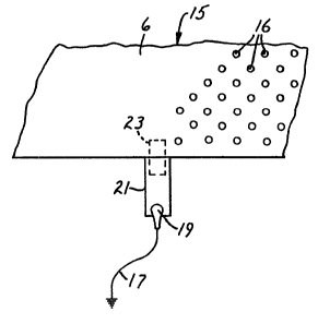
Referring now to Figure 3, there is illustrated
a width of tape 5 positioned as a floor runner 15 and
adhered to a floor by the adhesive coating. The tape 5 has
the conductive layer, such as layer ~, ~oined by a ground
line 17 to a suitable conductor at ground potential. The
line 17 is connected by a terminal such as part number
52584 from AMP Incorporated, Morristown, Pennsylvania, to a
thin strip 21 of the tape 5. The strip 21 is joined
physically and electrically to the runner 15 by a strip of
aluminum foil tape 23 which is adhered to the conductive
layer of the runner 15 and strip 21. The tape 23 is tape
No. 429 available from Minnesota Mining and Manufacturing
Company, St. Paul, Minnesota.
Having thus described the present invention with
respect to a description thereof, what is claimed is as
~ollow~.
. .
, . , , , . . : ~: ., , : :