Note: Descriptions are shown in the official language in which they were submitted.
132~82
W~E. 54,510
Electro-Optical Voltage Measuring System Incorporating A
Method and Apparatus to Derive the Measured Voltage
Waveform from Two Phase Shlfted Electrical Signal
Backqround of Invention
Field of Invention
This invention relate~ to an electro-optical
system for accurately deter~ining the electrical voltage
between two spaced objects. More specifically, the
invent1on relaSes to a syqtem which utilize~ an electro-
optical crystal with a fourfold axis of rotary inversion
which exh1bits birefringence in proportion to the magnitude
of an applied eleçtric field. In particular, it relates to
generating two electrical signals in quadrature from
parallel beams of collimated polarized light whlch are
pa~ced through the electro-optical crystal and retarded by
fractlonal waveplates to produce a relative retardation of
1/4 wave. Finally, the invention relates to deriving a
representation of the voltage waveform generating the field
applied to the electro-optic crystal from the two electrical
slgnal~ in quadrature utilizing a digi~al computer.
Background Information
~lectro-optical systems for measuring electric
voltages are known. For instance, devices known as Pockel
cells utilize cer~ain crystals which exhibit birefringence,
that is a difference in the index of refrac~ion in two
orthogonal planes, in the presence of an electric field.
Some of these crystals, such as, for example, RDP (po~assium
1328~
- W.E. 54,510
dlhydrogen phosphate), have a fourfold axis of rotary
inverslon. Such materials have the property that in the
absence of an electrlc field the index of refraction for
light propagating along the fourfold axis lS independent of
the plane of polarization of the light. However, if an
electric fleld is applied parallel to the direction of the
light, the index of refraction for light polarized in one
direction transverse to the fourfold axis, known as the fast
axis increases and that in an orthogonal dlrection, also
transverse to the fourfo}d axis, and known as the slow axis,
decreases by an amount which i proportional to the strength
of the electrlc field. In such Pockel cell devices, if
light is polarized in a plane-which forms an angle to these
transverse axes, the component of the polarized llght in the
direction of the slow a~is with the decreased index of
refraction is retarded with respect to the other
component. If the crystal is aligned with its fourfold axis
extending between the objects between which the voltage is
to be measured, and the polarized light is directed parallel
to the fourfold axis, the total retardation will be
proportional to the total voltage differential between the
two ob~ects. This retardation is typically measured ln
wavelengths. The retardation is detec~ed in an analyzer and
converted to an electrical signal for producing an output
representative of the magnitude of the voltage generating
the field Due to the cylic nature of this electrlcal
slgnal, the output is only unambiguous for voltages
producing a retardation which is less than the half wave
voltage for the cry~tal. In RDP, this half wave voltage is
about 11300 volts. Thls type of devlce is therefore not
sultable for measuring transmi~sion line voltages whlch can
be 100,000 volts rms and more.
Other types of crystals used in Pockel cells
respond to an electric field in a direction perpendicular to
1 3 2 8 ~ ~ ~.B. 54,510
-3-
the directlon of propagation of light through the cell.
Such cells only provide an indication of the potential at
the intersection of the beam with the field. Thus, a slngle
cell cannot integrate the potential over the full space
between two objects, and therefore these devices do not
provide an accurate measurement of the voltage between the
two objects. Systems using this type of Pockel cell
commonly either, (1) measure the potential at one polnt and
assume that the potential at all other points between the
two objects can be derived from this single measurement, or
(2) provide some sort of voltage dlvider and apply a fixed
fraction of the line voltage to the cell in an arrangement
which malntains the field within the cell constant. The
problem with the first approach is that except for low
impedance paths, the field along a path is sensitive to the
locatlon of any conducting or dielectric bodies in the
vicinlty of the path. Thus, if thi~ type of Pockel cell is
mounted on the surface of a conductor and the field
measured, the readinq would depend on the size and shape of
~0 the conductor, on the distance from the conductor to ground,
on the location and potential of any nearby conductors, on
; the location of any insulating or conducting bodies near the
sensor or on the ground beneath the sensor, and on the
presence of any birds, rain droplet or ~now between the
sensor and ground. Thus, only under very ideal
circumstances would accurate measurements be possible with
such a system. The problem with the second approach is in
- providing an accurate stable voltage divider.
Optical voltage measuring systems are desirable
because they provide good isolation from the voltage being
measured. Through the use of optic fiber cables, it is
possible to easily and convenlently provide remote
indicators which are not subject to the electrical
disturbances which remote indicators fed by electrical
3s slgnals must contend ~ith.
13284~2
W.E. 54,510
There remains, however, a need for an optical
system for accurately measuring very large voltages such as,
for example, those present in electrical transmission
systems without the use of a voltage divider.
Subordinate to this need lS a need for such an
optical system which can integrate the field over the entire
space between the ob;ects, such as in the case of the
electrical tran~mlssion system between line and ground.
Summarv of the Invention
These and other needs are satisfled by the
inventlon which i8 directed to a method and apparatus for
measuring an electrical potential between two spaced apart
objects utilizing a cry~tal havlng a fourfold axi of rotary
inverslon extending between the spaced apart objects.
Collimated light polarized with a plane of polarization
forming an acute angle to the fast and slow axes of the
crystal by first polarizlng mean~ is directed through the
crystal parallel to the fourfold axis of rotary inversion.
Retardatlon, due to the electric field, of the polarlzed
collimated light passed through the crystal, is detected by
addltional polarizing means. The light emerging form the
additional polarizing means is converted to electrical
qignals by photodetectors. To eliminate ambiguitie~ in the
measurement of voltages which exceed the half-wave voltage
of the crystal, a first portion of the polarized colllmated
light is retarded with respect to a second portlon.
Preferably, this retardation is 1/4 wave 50 that the two
electrical signals generated from the two portions of
polarized collimated light are in guadrature.
Preferably, the collimated light is ~enerated by
two separate light sources. The parallel collimated light
beams produced by these two sources are polarized by the
first polarized means and pass through the electro-optic
crystal to f~rm th~F first and second portions of the
132~4~2
W.E. 54,510
polarized collimated llght which ~re converted into the two
electrical signals. The intensities of these light sources
for the two beams are regulated by feedback circuits to
maintaln the peak to peak values of the two electrical
signals constant and equal.
One feature of the invention is a method and
apparatus for derlving a waveform representative of an
orlginal waveform, such as the voltage generating the field
applied to the crystal in the voltage measuring system, from
two phase shifted electrical signals such as the two
constant peak amplitude electrical signals generated by the
photodetectors in the voltage measuring system. In one
sense, the original waveform is reconstructed from selected
segmentQ of the two electrical signals with the segments
selected ln part as a function of the sequence of zero
crossings of the two electrical signals. At another level,
th~ representative waveform can be constructed as a
stairstep signal having discrete incremental values whlch
increment or decrement with each zero crossing depending
upon which of the two electrical signal3 is leading.
Reversal of direction of the measured waveform can be
detected, for instance, from two zero crossings in
succe~sion by one of the two electrical signals.
While ~uch a stairstep waveform may be adequate
for many applications, the accuracy of such a signal does
not reach the 0.1~ desired in the measurement of
transmi~sion line voltages which, for example, can be
260,000 volts peak to peak or 93,000 volts rms.
Accordingly, the invention includes interpolating between
steps of the stairstep waveform using the lnstantaneous
value of a selected one of the two electrical signals. The
value of the electrical signal which is smaller ln magnltude
is always selected for the interpolation. This results in
utilization o~ portio~s of the component waveforms where the
132~482
6 -- ~
small angle approximation, that is where the sine of
the angle is approximately equal to the angle, is
valid, and hence the errors introduced by the
interpolation are small.
In order to eliminate erratic indexing of
the zero crossing count for random behavior of the
electrical signals around zero, a dead band is
centered on the zero axis of the electrical signals.
When the value of the smaller electrical signal
enters this dead band, indexing of the zero crossing
count is suspended until the signal emerges from the
band. If it exits on the opposite side of the band
from which it entered, the zero crossing count is
indexed. Whether it is incremented or decremented
depends upon the direction in which the original
waveform is moving, which is manifested by which of
the quadrature electrical signals is leading. If
the electrical signal of smaller magnitude exits on
the same side of the dead band as it entered, the
measured waveform has changed direction and the zero
crossing count is not indexed. Preferably, the
magnitude of the electrical signal required to exit
the dead band is greater than that required to
- enter. This hystereses in the width of the dead
band prevents erratic behavior at the boundaries.
While this reconstruction of a waveform
from phase shifted electrical signals is
particularly suitable for use in the opto-electrical
system, which is also part of the invention, for
generating waveforms representative of sinusoidal
voltage waveforms of large magnitude, it also has
applicability to reconstructing other types of
waveforms in other applications.
~ ' ~
132~82
- 6a -
In accordance with a particular embodi-
ment of the invention there is provided an apparatus
for measuring an electric potential between two
spaced apart objects, said apparatus comprising:
light source means generating collimated
light;
first polarizing means polarizing said
collimated light to form polarized collimated light;
an electro-optic crystal having a fourfold
axis of rotary inversion extending between said
spaced apart conducting objects, said polarized
collimated light passing through said electro-optic
crystal in a direction parallel to said fourfold
axis of rotary inversion;
fractional waveplate means through which
at least a first portion of said polarized
collimated light passes after passing through said
crystal, said fractional waveplate means retarding
said first portion of polarized collimated light
- 20 about an odd multiple of % wave with respect to the
second portion of said polarized collimated light;
second polarizing means through which said
first and second portions of said polarized
collimated light pass after passing through said
: 25 crystal and said at least one portion thereof passes
through the fractional waveplate means;
first and second detectors converting said
first and second portions of said polarized
collimated light emerging from said second
polarizing means into first and second electrical
signals respectively; and
output signal generating means for
generating an output signal representative of the
potential between said two spaced apart objects from
said first and second electrical signals.
~ A
~32~$s~
- 6b -
In accordance with a further particular
embodiment of the invention, there is provided a
method of measuring electrical voltage between two
spaced objects comprising the steps of:
positioning an electro-optic crystal
exhibiting birefringence in two orthogonal axes
transverse to an optical axis in response to an
electric field, with said optical axis extending
betwèen said two objects;
generating collimated light polarized with
a selected plane of polarization;
passing the polarized collimated light
through said crystal parallel to the optical axis
and with the plane of polarization of the polarized
collimated light at a selected angle to said two
orthogonal axes of the crystal;
retarding a first portion of said
polarized collimated light emerging from said
crystal with respect to a second portion;
passing the two portions of polarized
collimated light after the first has been retardéd
relative to the second through polarizing means;
converting the two portions of said
polarized collimated light as they emerge from the
polarizing means into first and second phase shifted
electrical signals; and
generating an output signal representative
of the voltage between said two spaced objects from
said two phase shifted electrical signals.
Brief Description of the Drawinqs
A full understanding of the invention can
be gained from the following description of the
preferred embodiment when read in conjunction with
the accompanying drawings in which:
L ~.
~328~82
W.E. 54,510
Figure l i8 a schematic diagram illustrating the
princlple of operation of voltage measuring systems which
form a part of the invention.
Figure 2 is a schematic diagram of a voltage
measuring system in accordance with the invention.
Figures 3a, b and c are waveform diagrams
lllustratlng respectively the line to ground voltage to be
meas~red, the waveforms of the phase shifted electrical
signals generated by the opto-electrlcal measurement system
of Figure 2, and the output waveform reconstructed from the
phase shifted electrical waveforms.
Figure 4 is a diagram illu~trating how ~he ou~put
waveform is reconstructed from the phase shifted electrical
waveforms.
Figure 5 is a flow chart illustrating the program
used by the system of Figure 2 to construct the output
waveform from the phase shifted electrical waveforms in the
manner illustrated in Figure 4.
Figure 6 is an isometric view with part broken
away of apparatus for measuring line to ground voltages in a
hlgh voltage electric power transmission system in
accordance with the invention.
Figure 7 lS an enlargement of a subassembly of
Figure 6.
2S Figure 8 is a vertlcal section through a component
which ~s part of the subassembly of Figure 7.
Descrip~ion of the Preferred Embodiments
As is known, the voltage between two spaced
points a and b is defined by the equatlon:
~ ( ) (Eq. l)
., ~
1 3 2 ~ a ~ 2 W.E. 54,510
where E(x) is the field gradient at x and tbe integral is
lndependent of path. Thus, in order to accurately measure
the voltage between spaced points a and b, it is necessary
that a sensor physically extend from a to b, interact with
S the field at every point along its length, and change some
property so that some parameter varies in an additlve
fashion allowing the integral to be evaluated. In the
measurement of tran~mission line voltages, this requires
that one end of a sensor be electrically connected to ~he
transmission line and the other end be electrically
connected to ground. m us, the -~ensor must be of sufficient
length to withstand normal line voltages and any surge~
which might be encountered.
The present invention utilizes an electro-optic
crystal to measure the integral of the field gradient from
point a to b and thus provides a true value for the voltage
between a and b. As mentioned previously, certain
crystaline materials having a fourfold axis of rotary
lnversion, such as KDP (potassium dihydrogen pho~phate),
have the property that in the absence of an electrical
field, the index of refraction for light propagating along
the fourfold axis is independent of the directlon of
polarization of the light. However, if an electric field is
applied parallel to the direction of propagation of the
light, the index of refraction for light polarized in a
given direction perpendicular~to the fourfold axis increases
while the index of refraction of light polarized in a
perpendlcular direction decreases by an amount which is
proportional to the field. In RDP, the direction parallel
to the fourfold axis, which is al~o called the optic axis,
is commonly designated as the ~ direction, and the
orientations of the polarizatlon for which the maximum
changes in refractive index witb electric field are observed
are commonly designated as the X and Y directions.
",i
132~
W.E. 54,510
_g_
To understand the principle of operation of such
an opto-electrical sensor, reference is made to Figure l.
In the conventional ~ockel cell device l, a RDP crystal 3 is
aligned with its fourfold axis of rotary inversion, Z,
s parallel to the field gradient, Fg to be measured. A single
beam of unpolarized light is incident on a first linear
polarizer 7. The crystal 3 and first polarizer 7 are
arranged such that collimated polarized light, 5p exiting
the polarizer is propagating parallel to the Z a~ls of the
crystal and the plane of polarization of the light is at an
angle of 45 degrees to the X and Y axes of the crystal.
The incident polarized beam 5p can be decomposed
into two component~ of equal intensity, one polarized
parallel to the X axis and the other polarized parallel to
the Y axis. In the absence of an e}ectric fleld, these two
components will propagate with egual velocities and exit the
crystal 3 in phase with one another. When an electric field
is applied along the Z axis of the crystal, the refractive
indexes, and, as a result, the velocities of the two
zo components will not be equal, and there will be a phase
shlft or a retardation between the two components when they
exit the cry~tal. Since the retardation in any small
element along the crystal is proportional to the electric
field acting on that element multiplied by the length of the
element, and the total retardation is equal to the sum of
the retardations in all of the elements along the crystal,
retardation of the components exiting the crystal is
proportional to ~ Edl, and thus the difference in voltage
between the two ends of the crystal.
The retardation is usually expressed in
wavelengths, that is a retardatlon of one means the optical
path in the crystal lS one wavelength longer for one of the
components of the beam 5p than for the other, and is given
by the equatio~: _
132~2 W.E. 54,510
--10--
r _ r63 n x V (Eq. 2)
where r63 i5 an electro-optic coefficient, ng, is the
refractlve index for light propagating along the Z axis,
lg the wavelength of the light in vacuum~ and V is the
dlfference in voltage in the two ends of the of the
crystal. While these parameters are known and the
retardation can be calculated, it is usually more convenient
to combine them in a single parameter, the half-wave
voltage, Vh, defined by the equation:
Vh ~ ~ (Eq. 3)
2 r63 n
and thus:
r ~ v (Eq. 4)
Vh
Vh is usually determined a~ part of the calibration of the
sensor. If the two component~ of t~e beam 5p exiting the
crystal are pa~ed through a second polarizer 9 oriented
parallel to the first, the intensity of the bea~ I exiting
the polarizer 9 i8 related to the retardation by equation:
I s Io Cos2 (~ r ) ( Eq. 5)
where Io i~ the intensity of the exiting beam with zero
retardation: That is, with no voltage difference between
?5 the ends of the crystal. If the second polarizer 9 is
rotated 90 degrees, then I is qiven by equation 5 in which
the square of the sine function is substituted for the
square of the cosine function.
It is common in such Pockel cell devices described
to this point to insert a fractional wave plate ll between
the crystal ~nd th~ second polarizer 9 to shift the
13~ 82
-11- W.E. 54,510
retardatlon to a linear point on the sine or cosine squared
function.
8ecause of the periodic properties of the sine and
cosine functions, a device as discussed to this polnt would
only provide unambiguous results for voltages less than
Vh. For KDP, at a wavelength of 800nm, Vh is roughly 11,300
volts, and thus such a device cannot be used to measuce
transmission line voltages which are typically around
100,000 volts rms line to ground or more.
In order to resolve the ambiguities inherent in
the conventional Pockel cell arrangement, and allow
measurements at transmission line voltages, the present
inventlon utilizes a second llght beam 13 parallel to the
beam 5. This second light beam 13 is polarized by the first
polarizer 7 to form a second polarlzed light beam 13p which
is passed through the cry~tal 3 parallel to the Z axis.
This second polarized light beam 13p can also be resolved
lntO two components, one parallel to the Z axis and the
other parallel to the Y axis. The second beam exit~ng the
crystal 3 is al w passed through the second polarizer 9 so
that the intensity of the second beam exiting polar1zer 9 is
also related to the retardation by equation 5 if the second
polarizer is oriented parallel to the first polarizer 7 or
by the sine squared function if the second polarizer is
orthogonal to the first polarizer. The second light beam 13
exitlng the crystal 3 is also retarded by a fractional wave
plate 15 before passing through the second polarizer 9. The
fractional wave plates 11 and 15 are selected 50 that one
beam is retarded with respect to the other. In the
preferred form of the invention, the one beam i5 retarded
1/4 wave with respect to the other so that the beams e~lting-
the second polarizer are ln quadra~ure. This retardation
may be accomplished by utilizing one-eighth wave plates for
the fractiona~ wave ~ates 11 and 13 with their axes 17 and
-
132~82
-12- W.E, 54,510
19 respectively oriented 90 degrees with respect to one
another. Other arrangements can be used to retard the one
light beam 1/4 wave with respect to the other. For
instance, one beam could be passed through a quarter wave
plate while the other passes directly from the crystal to
the second polarizer. Retarding one beam exactly 1/4 wave
with respect to the other simplifie3 the calculation
requlred, but as long as the retardatlon is about 1/4 wave,
meaning within about plus or minus 20~ of 1/4 wave,
satisfactory re~ults can- be achieved. In addition to 1/4
wave retardation, odd multlples of 1/4 wave can also be u~ed
i.e., 3/4, 5/4 et cetera.
With the two one-eighth wave plates oriented as
indicated in Figure 2, the intensities of the two beams
exiting the second polarizer can be determined as follows:
I1- Io Co~2 ( ~ r ~ ~/8) (Eq. 6)
and
I2~ Io Co~2 ( ~ r - ~/8) ~Eq. 7)
These two signals are in quadrature and, with the exceptlon
of a con~tant, allow the unambiguou~ determination of the
voltage applied to the crystal.
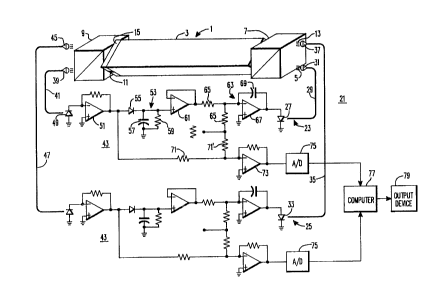
Figure 2 illustrates schematically a complete
voltage measuring system in accordance with the invention.
This system 21 includes the sensor 1 comprising the crystal
3, the first and second polarizers 7 and 9 respectively, and
the one-eighth wave plates 11 and 15. The system 21 also
includes first and second light sources 23 and 25 which
generate the two collimated light beams 5 and 13
respectively. The light source 23 includes a light emitting
dlode ~LE~) 27. Light produced by the LED 27 is transmitted
by OptlC fiber cable 29 and passed through collimating lens
31 to produce~the fi~st collimated light beam 5. Similarly
132~82
W.E. 54,510
-13-
the LED 33 in second light source 25 produces light which is
transmltted by the optic fiber cable 35 and passed through
colllmating lens 37 to produce the second colllmated light
beam 13. Light from the first beam 5 exlting the second
S polarizer 9 is gathered by lens 39 and conducted through
fibee optic cable 41 to a first electronic circuit 43.
Similarly, the second beam exiting the second polarizer 9 lS
focused by lens 45 on fiber optic cable 47 which directs the
light to a second electronic circuit 43.
The electronic circuits 43 are identical and
include a photo diode 49 which converts the light beam
carried by the optic fiber cables 41 or 47 respectlvely into
an electrical current. The electronic circuits 43 include a
transimpedance amplifier 51 which provide~ a low impedance
input to a peak detector 53. Peak detector 53 includes a
diode 55 which feeds a capacitor 57 shunted by leak resistor
59. The peak detector also includes a buffer amplifier 61
to prevent the peak detector from being loaded by the
followinq stage. m e following stage 63 acts as a summing
amplifier, integrator, and a driver for the reYpective LED
27 or 33. It includes a pair of reslstors 65, and an
operational amplifier 67 shunted by an integrating capacitor
69. An output circuit includes a pair of resistors 71 and
71' (egual to twice 71 in value), and an output ampllfier
73. A reference voltage -er is applied to the summlng
circuits formed by the resistors 65 and 71-71'.
The electronic circuits 43 operate as follows:
Light exiting the second polarizer 9 and transmitted via the
optic flber cable 41 or 47 respectively lS converted to an
electrical current signal by the photo diode 49. The peak
detector 53 generates a signal which repre ents the peak
value of this electrical current. The peak value slgnal lS
compared with the reference signal through the resistors 65
connected to~ the ~verting inpu~ of the operational
132~2 W.E. 54,510
-14-
amplif1er 67. Since the diode 55 assures that the peak
s signal 1S posltive, and since the reference signal -er lS
negative, these two signals are compared and the error
between the two is applled to the integrator formed by the
operational amplifier 67 and the capacitor 69. Thls
integrated error signal is used to drive the LED 27 or 33
respectively of the light sources for the first and second
llght beams. Thus, the c1rcuits 43 are feedback circuits
which regulate the intensity of the respective light beam so
that the peak values of the current signals generated by
these light beams through the photo detectors 49 remain
constant and equal to the reference voltage and, hence,
equal to each other. m e summing a~plifier 73 and voltage
dividing resistors 71 subtract the reference voltage from
the unidirectional currents produced by the photodetectors
49 to produce bipolar voltage output signals el and e2
respectively in respon4e to the field applied to the crystal
3. The analog signals el and e2 are periodically sampled
by an analog to digital converter 75 for input into a
dlg1tal computer 77. The digital computer 77 reconstructs
the voltage waveform from the two signals el and e2 for
presentation on an output device 79. The output device 79
can be, for instance, a digital readout, and/or can be a
recorder which generates a permanent log of the measured
voltage wavefor~.
Waveforms a, b and c of Figure 3 illustrate on a
comparative time basis the voltage waveform VI to be
measured, the quadrature electrical signals el and e2
generated ln response to the voltage waveform a by the
system of Figure 2, and the output wavefor~ V~ generated by
the system of Figure 2 which is representative of the
voltage waveform a.
Figure 4 illustrates the manner 1n whlch the
waveform c in~ Figure- 3 is constructed from the quadrature
1 3 2 8~8 2 W E. 54,510
-15-
electrical signals el and e2 forming the waveform b in
Figure 3. Essentially the method comprises maintaining a
bldirectional count of the number of zero crosslngs of the
two electrical signals el and e2. In the example given in
Figure 4, the count, n of such zero crossings is ~hown
across the top of the figure. The count n is incremented as
the voltage waveform repre5ented by e1 and e2 is becomlng
more posltive (or less negative) and i5 decremented as the
magnltude of the incremented waveform is becoming more
negat1ve (or less positive). The directlon ln which the
waveform is moving is determined by which of the quadrature
signals is leading. Reversal of the direction of the
voltage waveform resultQ in a switch in which signal el or
e2 lg leading and can be detected by two successive zero
crossings by the same signal el or e2.
A stairstep approximation of the voltage waveform
indicated by the trace 81 in Figure 4 can be generated from
the cumulative count n of the zero crossinge. In the
particular sample shown, the output Qtairstep waveform i8
generated as a function of twice the accumulated count n as
shown by the scale on the left side of the trace 81 in
Figure 4.
This stairstep approximation 81 of the original
voltage waveform generating the field applied to the opto-
electrical sensor can be adequate for many purposes.
~owever, where more accurate reproduction of the original
voltage waveform i5 required, such as in monitorlng the
voltage of high power transmission lines where an accuracy
of 0.1 percent is required, interpolation must be made
between the stairstep values of the output signals
generated by the accumulated zero crossing count n. Thls
smoothing of the output waveform is achieved by adding or
subtracting the instantaneous value of a selected one of the
quadrature sigrals e~and e2 to the stairstep value. The
1328~2 W.E. 54,510
selected signal lS the one of the two signals, el and e2,
which is smaller in magnitude at the given instant. Thus,
the magnltude of the signal el or e2 whlch is between the
traces 83 and 85 in Figure 4 is selected. This results in
utilization of portions of the waveforms el and e2, where
the small angle approximation, that is, where the slne of
the angle is approximately equal to the angle, 1S valid. As
can be seen in Figure 4, the technique essentially results
in the stringing together of the segments of the quadrature
signals el and e2 to reconstruct the original voltage
waveform.
In order to avoid random indexing of the
bidirectional cumulative count n of zero crossingR which
could occur with small signal~, a band is created around the
zero axis a~ indicated by the lines 89 and 91 in Figure 4.
Zero crossings are not counted while a signal el or e2 is in
this dead band. Instead, a determlnation i3 made when the
signal again leaves the dead band as to whether the zero
crossing n should be indexed. If the quadrature signal
exits the dead band on the same side that it enteced, then
the target signal has changed direction and n should not be
indexed. If the quadrature signal exits the dead band on
the oppoqite side from which it entered, then there has been
a zero crossing and n is indexed. While a ~uadrature slgnal
is within the dead band, its magnitude is continued to be
used to interpolate between the stairsteps. If the
quadrature signal crosses the zero axis, the sign of the
increment which is added or subtracted to the stairstep is
changed to reflect this transition. This delay in the
indexing of the zero crossing count n until the quadrature
signal leaves the dead band results ln a slight shift in
tlme of the stairstep slgnal, as indlcated at 93 in
Figure 4. The width of the dead band should be set as wide
as possible without having the instantaneous values of both
~ Y~
1 3 2 ~ w. E. 54,510
el and e2 fall within the band at anytime. Preferably, the
boundaries of the dead band are expanded to 89'-91' once a
signal is within the band. This introduces hysteresis into
the dead band which aids in assuring a positive transition
s lnto and out of the dead band.
Pigures 5a and 5b constitute a flow chart of the
program employed by the digital computer 77 to reconstruct
the voltage waveform sensed by the sensor from the
quadrature electrical signals el and e2, in the manner
dlscussed in connection in Figure 4. As discussed
previously, the analog quadrature signals el and e2 are
applied to an analog to digital converter to generate
digitaL samples of the instantaneous value of these
waveforms for processing by the digital computer. The
sampling rate should be sufficiently rapid that, at the
maximum slew rate of the voltage ~ignal being measured,
which usually occurs at the its zero crossing, at least one
data sample for el or e2 falls within he dead band. The
sampling rate for the 60 hz voltage-signal was 400 KHz in
the exemplary system. As indicated at block 101 in Figure
5a, the program waits for each new data sample. Two
varlables, El and E2, are set equal to the current
instantaneous value of the quadrature signals el and e2
respectively at 103 when each new data sample is acqulred.
Another variable S which indicate~ whether the signs of the
current values of El and E2 are the same is set, and that
indication is saved as an additional variable SS in block
105.
A flag Ql~ which has a value of 1 if the preceding
El was inside the dead band defined by the lines 89-91
(entering) and 89'-91' (exiting) in Figure 4, is checked
block 107. If the preceding El was inslde the band and ~he
present value of the first guadrature signaL remains inslde
the band as ~determined in block 109 (using the larger
132~82 W.E. 54,510
-18-
boundary of llnes 89'-91' equal to 0.24 ER), then the
variable S, which wlll be recalled lS an ind~catlon of
whether the signs of El and E2 are the same, is set at 111
equal to S0 which is the value of S for the preceding data
S point.
If El has emerged from the dead band, then the
flag Ql is made e~ual to zero at 113 and it becomes
necessary to determine whether the zero crossing count, n,
should be indexed, and if so, in which direction. Thi~ lS
accomplished by setting another variable A at 115 to
lndicate whether the sign of the present El is equal to the
sign of Eloo which i~ the last value of El before El entered
the dead band. For the purpose of this determination, the
slgn of El is +1 if El has a po itive value, or -1 if it has
a negative value so that A can have a value of -2, +2 or
zero. If the signs of El and Eloo are the same as
determined in block 117, El has emerged from the ~ame ~ide
of the dead band at which it entered and hence there has
been no zero cro~sing. If the~e ~ign~ are not the same,
then El has emerged from the oppoaite ~ide of the dead band
from which it entered and hence there wa~ a zero crossing
and n mu~t be indexed. If the sign of A i~ the -Rame as the
sign P ~2 as determined in block 119 then the voltage is
golng up and a variable D is set equal to one at 121. If
the_e sign~ are not equal, then the voltage is going down
and D i~ set a~ equal to minu~ one at 123. The cumulative
zero crossing count n is then indexed in the proper
dlrection at block 125.
If it wa~ determined back at block 107 that the
preceding lnstantaneous value of El was outside the dead
band, then a check is made at 127 to determlne if the
present value of El is within the dead band (using the
narrower boundary defined by lines 89-91 ln Figure 4). If
El is now in ~he dea~ band, then the flag Ql is ~ade equal
13~ 2 w. E. 54,510
--19--
to one, Eloo wh~ch is a variable equal to the last value of
El before the band was entered is made equal to Elo whlch is
the preceding value of E1, and S which, it will be recalled,
is an indication of whether the cigns of El and E2 are the
same is made equal to S0 which is the value of S for the
last point, all as indicated at block 129. If El remains
outs~de of the dead band, then a determination is made at
block 131 as to whether the preceding value of E2 wa~
outside the band. If it was, and the present value of E2 lS
wlthln the band as determined at block 133 (using the
entering boundary lines 89-91 in Figure 4), then a flag Q2
is made equal to one, the last value of E2 before ~t went
into the band i3 saved, and S is made equal to S0 all in
block 135. If it was determined in block 133 that E2 was
not within the band, then both El and E2 remain outside the
dead band and the program proceeds to the calculation of the
present value of the voltage signal in the manner discussed
below.
If it was determined at 131 that E2 was inside the
band at the previous data point, a determination i8 made at
block 137 whether it is still within the band. If it lS, S
is set equal to S0 in 139. If E2 has now emerged from the
band, then the flag Q2 is set equal to zero at 141. A
determination i8 then made in blocks 143 and 145 using the
variable A in a manner similar to that described in
connection with blocks 115 and 117, to determine whether the
zero crossing count n should be indexed. If E2 has emerged
from the opposite side of the dead band from that from which
it entered, then n is incremented or decremented in box 147,
149, 151 and 153 using the same technique as described ln
connection with emergence of El from the dead band. That
lS, n is incremented lf waveform el leads e2 and hence the
voltage being measured is increasing, or n is decremented
when the measured voltage is decreasing.
132~82
W.E. 54,510
-20-
Turn~ng to Figure 5b, a determination is made inblock 155 whether there has been a zero crossing by
determinlng if SS, which is the saved sign, is equal to S,
which was set equal to S for the preceding data polnt if
ei~her El or E2 ~s currently in the band. IÇ there has been
a zero crossing, a variable P is set equal to mlnus one at
157, otherwise P is set equal to plus one at 159.
If El and E2 are not of the same sign as
determined in block 161 and E2 is of smaller magnitude as
determined in block 163, then a voltage EC is calculated
using the cumulative zero crossing count n and the current
magnitude E2 in the equation in block 165. However, if E
and E2 are not of the same sign but El is smaller than E2,
then El is used with n to calculate EC using the formula ln
block 167. When El and ~2 are of the same sign, as
determined at 161 and Bl is smaller, as determined at 16g,
then El is used with n to calculate the value of EC in block
171. On the other hand, if E2 is the smaller of the two
signals which are not of the same sign, then E2 ~3 used with
zo n to calculate EC in block 173. A~ will be noticed, the
f~rst term in the eguations for EC in blocks 165 through 171
determinea the stairstep value from the cumulative count of
zero crossing n, and the second term provides the
lnterpolation based upon the magnitude of the selected
quadrature signal.
The calculated voltage EC is then multiplied by a
scaling factor in block 173 to determine the instantaneous
magnitude, E, of the measured voltage.
It is convenient to chose er, the reference
voltage used in the electronic circuits, equal to 2.828
vol~s, so that that the quantity .3535 x er ~ 1 and 2 x
3535/er ~ 1/4 and hence the computations in blocks 165,
167, 171, 173 and 175 are simplified.
-- .,
132~2
W.E. 54,510
-21-
The measured voltage is unambiguously determlned
by this procedure except for a constant error. This error
is the result of the uncertainty of the initial value of n
when the program is started. It is noted that n is an
5integer but-otherwise arbitrary. If n can be set equal zero
when the voltage is zero, then qubseguent voltage
measurements will be correct. In general this is not
posqible and one must adjust n ln integer steps until the
. average value of the calculated voltage over one cycle is
10zero. After n is properly adjusted, the calculated voltages
will be correct until the program is interrupted.
The program is completed by ~toring the pre ent
values of S, El and E2 as the last value in block 177 in
preparation for the next computation of E. The program then
15loops back to the beginning and waits for the next input of
data.
Figures 6 through 8 illustrate a practical
embodlment of a sensor 1, mounted in an insulation column
201 which is cut away to show the mounting of the sensor.
20An upper supporting tube 203 is connected to a transmission
line (not Qhown) and a lower supporting tube 205 is
connected to ground. Both tubes are electrically conductlng
and provide contact between the ends to the sensor 1 and the
line and ground respectively through mounting discs 207
25constructed from electrlcally conductiPq transparent
material such as NES~ glass. Cry~tal 209 and the polarizers
211 and 213 are made with a circular cross ~ection rather
than square a-~ in Figure 1 and 2 to reduce the electrical
stresses.
30As shown more clearly in Figure 7 for the second
polarizer 213, two cylindrical collimators 215 are mounted
on one flat end face of the cylindrical polarizer and
rectangular one-eighth wave plates 217 and 219 are mounted
against the op~osite ~nd. The collimators 215, which focus
1~2~482
-22- W.E. 54,510
the llght beams received from the second polarizer 213 on
the optic fiber cables 221, are shown broken away in
Flgure 8. Each collimator 215 is formed from two pieces 223
and 22~ of low refractive index glas~, such as fused sllica
and one piece of hlgh index glass 227 such as SF59. The
radius of the curved surface of 227, the thickness of 227
and the length of 225 are chosen so that a bundle of
parallel light entering 223 is focused on to the end of
optic fiber 221 and the rays from the edge of the bundle
str1ke the fiber. More particularly, these parameters a
chosen so that the radius of the bundle of light divided by
the focal length of the lens is equal to or greater than the
numer1cal aperture of the flber divided by the refractive
index of the lower refractive index glass. The colllmators
at the other end of the ~ensor are similarly designed, but
operate in the reverse direction to transform light received
from the fiber optic cable into the bundle of parallel light
which is passed theough the first polarizer 211. Thl~ form
of a collimator is necessary since in order to withstand the
~0 h1gh electrical stresses during operation, and especially
lmpulse test~, the in~ulator 201 is filled with oil or
pressurized sulfur hexafluroide (SF6), and thus the optical
system cannot have any glass air interfaces.
While specific embodiments of the invention have
been described in detail, it will be appreciated by those
skilled in the art ~hat variou~ modifications and
alternatives to those details could be developed in light of
the overall teachings of the disclosure. Accordingly, the
particular arrangements disclosed are meant to be
illustrative only and not limiting as to the scope of the
invention which is to be given the full breadth of the
appended clalms and any and all equivalents thereof.