Note: Descriptions are shown in the official language in which they were submitted.
ii 1 32~763
.,
~J
' _' 1 _
Th.is invention relates to color cathode ray
~ picture tubes, and ~.s: addressed specifically to an im-
¦s proved cataphoretic process for manufacturing color
!~ cathode ray tubes. T~e process is applica~le to the
.~ 5 manufacture of conventional color p~cture tu~es; that is,
-. tubes having a curved faceplate and a correlatively curved
shadow mask, and in the ~anufacture of color tu~es hav-
- ing shadow ~asks of the tens;`.on foil type mounted in as-
~ sociation with a flat or suhstantially-flat faceplate.
"7 10 Color tu~es of vari.ous types can be screened by the pro-
~ cess, including th.ose used ;n h.ome entertainment tele-
:,. vision receivers~. T~e cataphoretic process according to
~ the invention is particularly valuabIe in the manufacture
of medium-resolution, h~gh-re~olution, and ultra-high.
~- 15 resolution tubes intended for color monitors. To meet
. the requirement for h~.gh.resolution and h.igh.definition
. in such tubes, the phosphor elements must be extremely
.~ small and well defi.ned. T~e problems inh.erent in screen-
ing such tub.es ~s: pointed up by the fact that there are
2~ more than fiYe million such elements deposited on the
scréen of an ultxa-hi~h ~esQlution color tube. The de-
positing of so many elements is at the limit of capability
of conventional photoscreening proces-ses. The cataphoretic
~ process also. offers an economical benefit in that it is
. 25 much.less wasteful of the expensive phosphors used in
color screening.
Th~ conYentional process of depositing patterns
of color phDsphsr elements on the screening surface of a
color picture tube faceplate utilizes: th.e well-known
.
',
. ' :
,
1 328763
-- 2 --
.
-- photoscreening process. A shad~w-mask, w~ich in effect
functions as a perforated optical stencil, is used in
conjunction ~it~ a light source to expose in successive
~, steps, three discrete light-sensitive photoresist pat-
terns on the s-creening surface. The shadow mask is
typically "mated" to each faceplate; that is, the same
mask is used in the production of a specific tu~e through-
out the production process, and is permanently installed
in the tube in final assembly. At least four engagements
10 and four disengagements of the mask, as well as six
exposures, are required in the standard screening process.
In certain processes, a "master" may be used for exposing
the photoresist patterns in lieu of the mated shadow
mask.
i 15 In a typical photoscreening process, the
- screening surface is fixst coated with a fluidized light-
sensitive material to fabricate a ~rille, and which
hardens upon drying. The s~dow mask, mounted on a rigid
frame, is temporarily installed in precise relationship
- 20 to the faceplate, and the light-sensitive material is
exposed to light actinic to the coating projected through
the apertures of the mask from a light source located
` at a position that corresponds to the beam-emission point
of the associated electron gun of the end-product tube.
25 The faceplate is then separated fxom the shadow mask and
` the coating is 'Ideveloped~'' resulting in a hardened pat-
tern of openings in the grille. ~ slurry of dark surround
~ material is coated on the faceplate and the hardened
- resist is stripped, leaving a light-absorbing material
30 surrounding the areas where the phosphors are to ~e de-
posited. The red~ green and blue light em~tting phosphor
; elements are then sequentially deposited in respective
j grille openings with~a separate slurry of phosphor in a
light-sensitiye material for each color. The final pro-
35 duct is a faceplate having on its screening surface a
pattern of groups of dots or lines capable of emitting,
,~
L
.. . .. . . ... .. . .
.
- 3 - 1 32~763
upon excitation by electron beams, red, green or blue
light.
In U.S. Patent No. 4,130,472, Kaplan discloses a
process for making color television screens by electro-
phoretic deposition. The process comprises the depositing
of groups of periodically repeating electrically
conductive stripes of predetermined graduated length from
relatively long to relatively short on the screening
surface. Both ends of stripes of similar length are
electrically excited with a charge of first polarity
during immersion in an electrolytic bath that includes
color-image-related compounds charged to an opposite
polarity. Both ends of stripes of successively shorter
length are serially excited in conjunction with a
different bath and a different image-related compound. By
electrically contacting both ends of the stripes, the
effect of a single discontinuity in the electrically
conductivity of any stripes is nullified.
A process for electrostatically screening a color
cathode ray tube is disclosed by Lange et al in U.S.
Patent No. 3,475,169. In this process, the screening
surface is provided with a photoconductive surface to
establish thereon a uniform charge. A latent charge image
is then created in the photoconductor by exposing selected
portions to light actinic to the photoconductor. The
exposure of the photoconductor takes place through a
shadow mask so that areas which are to represent phosphor
elements of a particular color are selectively discharged
by the exposure. The latent image that results is
developed by the application of a toner that includes a
phosphor. The toner-phosphor responds to the electrical
fields of the photoconductor and is deposited on the
discharged areas. This process is repeated three times to
provide the three color phosphors necessary for the
cathode ray tube color image. A similar process is set
forth in British Patent Specification No. 1,242,999
published August, 1971.
.,
1 32~7 63
~ ~ 4
.
U.S. Patent No . 3, 681, 223 to Gupton discloses
means whereBy color phosph~rs are electrophoretically
, deposited on a cathode ray tube screening surface to pro-
vide a dot screen. A plurality of conductive dot patterns
5 are deposited on the faceplate, one pattern for each
? color to ~e deposited. Each pattern includes lands of
material on which the dots are to ~e deposited, with
- conductive paths interconnecting the lands. The con-
ductive patterns are deposited w~th a single masking
¦ 10 operation using an interchangea~le master. The d~fferent
color phosphor$ are then successively deposited on the
dot patterns by~ electrophores~$ r one color being deposited
on each discrete conductive pattern. me conductive paths
are said to ~e one mil wide. ~hile the ~lue- and green-
15 receiving patterns are indicated as ~eing relatively short,
the conductive path for the red phosphor is relatively
long--estimated to ~e ahQut 90~ fèet in a 25-inch color
picture tube. The problem of laying down a conductive
path of such lengt~ with an inter-dot width of only one
20 mil is considered to ~e insurmountable. A gap in the path
at any point ~ould halt electrophoresis along the un-
charged path; also, variations in voltage drop along the
narrow conductiye stripe could result in uneven deposits
of phosphor.
2~ In Canadian Patent No. 964,713, Standaart
discloses a process for the electrophoretic deposition of
color phosphors in a dot-screen pattern. A separate dot
pattern with an inter-connecting conductive path is pro-
vided for each color. An electrical potential is applied
to an end of each path ~y means of a selective clamping
dev;ce for the deposit~on of each color. The means for
applying the potenti~l are not disclosed. An interchangea~le
mask is used for the path depos~tion.
In a ~ournal article, Sadowsky descri~es the
35 preparation of lumlnescent screens, ~`ncluding deposition
,~
- 5 - 13287~3
by electrophDre~is, in which "the phosphor in li~uid
. suspension is attracted to an immersed electrode upon
; which.it depos~ts." S`adowsky comments: ".... there is not
much advantage to this method. I:t is uneconomical merely
to apply screens in th~.s manner, since screens of as
good a quality can more easily be depos.ited ~ other
means. The controls necessary on particle size, e.m.f.,
current, suspension, composition, temperature, etc., and
! the need for a conduct~ye substr~te militates against
10 its ues." ("The Preparation of Luminous Screens,"
! Meier Sadowsky, Society for Information Display,
. March.194~. Pages 119-12Q1.
I-n general this invention aims to provide an
improved process for the manufacture of color cathode ray
15 tubes using the cataphoretic process.
The present invention therefore provides
for use in the manufacture of a color cathode ray tube,
an improved cataphoretic process for depositing in sequence
.- on the screening surface of the tube faceplate at least
20 two separate patterns of substantially round phosphor
~ elements, with each pattern of elements capable of emitting
light of a different color when excited, th.e process
comprising first depositing an electrically conductive
coating over said screening surface for use as an electrode
i 25 during each.deposition operation, and secondly, depositing
~`. an electrically- insulative barrier over said conductive
coating and selectively and sequentially removing por-
tions of said barrier for controlling patterned, sequenced
cataphoretic access to said electrically conductive coating.
The improved process of the invention is ap-
plicable to most types of color cathode ray tubes, in-
cluding the conventional curved screen-curved faceplate
~. tuhe, as well as t~o tu~es. haYing a tensed foil shadow
:~ mask and a flat ~aceplate.
Among the advantages of the invention is that it
provides a more feasible and economical process for deposit-
ing screening =aterials on the screening surface of
.. . . . _ _ _ _, _ . _ _ . . . . . . ......... . .
,
' - 6 ~ 1 S? 87 ~ s
. cathode ray tuhes
Furthex features and a,dva.nta~es~of the pres-
` ent invention may best ~e understood ~.y reference to the
followi.ng descxiption of preferred em~odiments of the
5 invention taken in con~unct~on w~ith the accompanying
, drawings, in the several figures of which like reference
numerals identify like elements, and in which:
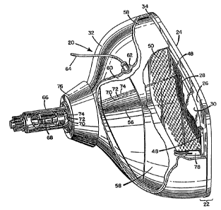
Figure 1 is a side view in perspective of acolor cathode ray tube havi.ng a flat faceplate and a
tensed foil shado~ mask~ with.cut-away sections that in-
dicate the locati.on and relati.on of the screen to other
v~ major tub.e comp~nent~;
~,. Figure 2 is a cut-away view in eIevation of a
~ color cathode ray tub,e.h.aving the conventional curved
; 15 faceplate and curved screen;
-, Figure 3 i.s a detail plan Yiew of the screen of
', a color cathsde. ray tu~e having a ,'!dot" screen;
',. Figure 4 is a view similar to Figure 3 except
; that the screen is a "line" screen sh.own with.associated
' 20 shadow-mask;
Figure 5 is, another view similar to Figures 3
~' and 4 except the screen sKown is the type th~t may ~e
'~ used in a ~eam index tu~.e;
Figure 6 is a view in ele~ation of a section of
-~ 25 a flat faceplate ~ith.a dot screen, and indicating the
screening area follow.ing preliminary steps in the cata-
' phoretic process according to the invention (Note: thR
.~ dot screen is. used as an example in the follow-ing descrip-
,, tion of th.e inventi.onl;
~, 30 Figure 7 ~s a sectional side-elevat~onal dia-
grammatical View~ of a 'lli.ghthouse" used for exposing the
. screening a~ea, ~n the screening process accord~ng to the
invention; th.e pho.toscreening of a flat tension mask
~ faceplate asse~ly i.s indicated ~y way of example;
'~ 35 Figure 8 i.s a i.n elevation of a section Qf the
;
; 7 1 3~8763
. faceplate sho~n by Figure 6, and indicating the imping-
. ing of light ~eamlets on selected areas o f the
~ screening surface of ~ dot screen during exposure of the
~ screen to ligh.t actinic to photosensitive areas as ac-
- 5 complished in the lighthouse depicted in Figure 7;
Figure 9 is a plan view of a section of a dot
screen faceplate following the exposure step indicated
by Figure 8; - ~-
Figure 10. is a schematic view in elevation of
10 a bath used in the c~taphoretic screening process ac-
^ cording to the i.nvention, and containing a section of the
faceplate shown hy Figure 9 as immersed in the ~ath.;
Figure 11 is a vi.ew in elevation of the section
of faceplate sh.own ~y Figure 9, with a ~ash-off spray
15 operation indicated diagrammat;`.cally;
- Figure 12 i6 a plan view o~ the section of the
faceplate sho~n b.y F~gure 9, showing the results of pre-
-; vious steps in the cataphQretic process according to the
invention;
~ 20 Figure 13 is a view similar to Figure 8 showing
... th.e selective impinging of light ~eamlets on the screen-
~:ing surface in another step in the process according to
the invention;
:-Figure 14 is a vie~ of a cataphoretic bath
25 similar to thR ~.ath of Figure ln, but showing a further
~-gstep in th.e process according to the invention;
Figure 15 depicts another step in the selective
~`impinging of ligh.t b.eamlets on the screening surface; and
Figures 16 and 17 are v~ews of cataphoretic
~-30 baths similar to the bath of Figure lQ, and depicting
`ifurther steps in the process- according to the in-
.~ vention.
The process according to the invention can b.e
used for the manufacture of various types of color cathode
~ 35 ray tubes includin~ tuhes having a tension foil shadow
:. mask in conjunction with a flat faceplate, and tubes
-
- "
`3
, ' '
.
8 ~ 1 3~763
having the conventional curved screen-curved mask tubes.
The operating principles of the two types are essentially
the same; that is, an electron gun projects three beams
through a color selection electrode to excite groups of
color phosphors emitting red, green or blue light when
excited by the respective electron beam.
A color cathode ray tube 20 having a tension foil
shadow mask is shown by Figure 1. The front assembly 22
includes a faceplate 24, on the screening surface of which
is deposited a phosphor screen 28. A film of aluminum 30
is indicated as covering the screen 28. A funnel 32 is
shown as mating with the peripheral sealing area 34 of
faceplate 24.
Front assembly 22 includes a shadow mask support
structure 48 for mounting a metal foil shadow mask 50
which is secured to support structure 48 in tension. The
round apertures shown in shadow mask 50 indicate that the
tube is a dot-screen type. The anterior-posterior axis of
tube 20 is indicated by reference number 56. A magnetic
shield 58 is shown as being enclosed within funnel 32.
High voltage for tube operation is applied to a conductive
coating 60 on the inner surface of funnel 32 by way of an
anode buttcn 62 connected in turn to a high-voltage
;
conductor 64.
The neck 66 of tube 20 is indicated as enclosing
and in-line electron gun 68, indicated as providing three
discrete in-line electron beams 70, 72 and 74 for exciting
respective red-light-emitting, green-light-emitting, and
blue-light-emitting phosphor elements on screen 28. Yoke
76 receives scanning signals and provides for the scanning
of beams 70, 72 and 74 across screen 28. A contact spring
78 provides an electrical path between the funnel coating
~ 60 and the mask support structure 48.
:.
~I S287~3
g
- With.reference now to Figure 2 there is shown
schematically a conventional color picture tube 80.
;~ Tube 80 is similar in form and function to the tube 20
, described in connection w-ith Figure 1 in th.at it has an
5 electron gun 82 that projects three beams 84 that conyerge
on the phosphor-bearing screen 86 of the faceplate 88
: after passing through a shadow mask 90 which, as has been
noted, provides for color selection. This configuration
differs however in that the faceplate 88 is curved,
lO as indicated, a.nd the shadow mask 90 is correlatively
curved. ~creen 86 may be.of the dot screen or line
screen type. Th.e ;mproved cataphoxetic process according
~' to th.e inyent~on may be used to deposit image-related
compounds on th.e screen 86 of th.is type of color cathode
~ 15 ray tube, noted as having a curved faceplate.
.~ Types of color picture cathode ray tube screens
on which.can be applied image-related compounds according
. to the invention are depicted in Figures 3-5. It is.noted
9 that the process according to the invention is not limited
20 to the examples shown as- other applications will readily
~- suggest the~selves to thDse skilled in th.e art.
The improved cataph.oretic process according to
the invention provides for depositing in sequence on thR
, screening surface of a color cathode ray tube at least
25 two separate patterns of phosphor elements. Figure 3
:.~ represents a dot screen 92 s.ho~n as having three such.
.~ patterns b.y ~ay-of example, and c.ompris-ing R, a red pat-
.i. tern, G, a green pa.ttern, and B, a blue pattern, with.each.
:. pattern capable of emitt~ng l~ght of the color designated.
30 The three patterns.--R, G, and B-- are distributed through-
~ out the screen. In a flat tension mask hav~ng a diagonal
-~ measure of 14.2 i.nch.es and a constant aperture pitch.of
-~ 0.2 millimeters, there are about 1,700,000 apertures.
Since each.aperture passes three beamlets--one beamlet
1 3~ for each.of the three patterns--there are about 5~loo~oQa
:
. . .
~ 32~763
-- 10 --
phosphor elements ~hich c~n be deposited on the screen-
ing surface by the cataphoretic process according to the
invention. So each pattern--R, G, and s--cons;sts of
1,700,000 phosphor elements. The patterns are grouped
-,~
5 in triads of red, green and blue, as indicated by triad
; 94, delineated by the dash~line outline, and the adjacent
triad 96.
.. . .
Dot-pattern screen 92 is depicted as including
a ligh*-absorptiYe, black surround material g8 also known
`~d lo as the "grille"; the hlack $urround is indicated sym-
bolically hy the stippling. T~e associated shadow
~ mask ~not shswn in thi:s examplel generally has apertures
-~ of the same round shape, with one aperture for each triad
~,...
i of phosphDr elements.
Figure 4 is a depiction of a line-screen pattern
104, with the ass-ociated shado~ mask 106 shswn to in-
dicate the yextically rectangular configuration of the
apertures 108~ The three electron beams 110, 112 and 114
are depicted as passing through a typical aperture 116
-~ 20 to selectively impinge upon respective blue-, red- and
i green-light-emitt~ng lines of phosphor 116, 118 and 120.
- An opaque, light-ahsorptive black-surround 122 is indicated
;ii ` as separating the lines of phosph~r.
~i Figure 5 is a view s~milar to Figures 3 and 4
25 except that a typical screen of a beam index tube is
depicted. Stripes 122, 124 and 126 are indicated sym-
' bolically as emitting green, red and hlue light when ex-
cited hy the h~rizontal trayerse of a single electron
beam (not shswnl. The stripes are depicted as being
30 separated by a hlack surround material 128, as indicated
by the stippling. ~n "Index" stripe 130 may comprise,
for example, an emitter of ultraviolet radiation used
to "index" th~ system; that is, to locate the beam in
relation to the phDsphor stripes 122, 124 and 126 across
which it passes.
These and other screen patterns not shown but
which function according to the same general principles
may be deposited hy the cataphsretic process according to
,~
.
l 3 ~ ~ 7 6 3
the invention.
~ In essence, the improved cataphoretic process
-- according to the inyention provides for the deposition in
.~ sequence on the.screening surface of the tube faceplate
at least two separate patte.rns of phosphor elements, with
~' each pattern of elements capable of emitti.ng ligh.t of a
different color wh.en excited. In the following descrip-
tion of the inyentive process, first, second and third
separate patterns of phDsphor elements are depicted which
10 are capable of emitting such. light when excited for
exemplary purposes, the s.eparate patterns are in-
dicated symb.olically as. being red-light-emitting, green-
.~ light-emitting, and blue-light-emitting phosphor elements.
: Ess.entially, the process according to the in-
15 vention comprises first depositing an electrically con-
ductive coating over the screening surface to serve as
an electrode. during each deposition operation, and
secondly, depositing an electrically insulative barrier
over the conductive coating and selectively and sequen-
20 tially removing portions of th.e barrier for controllingpatterned, sequenced cataphoretic access to the electrical-
ly conductive coating.
~ith.reference to F~gure 6, there is shown a
- section of a cathode ray tub.e faceplate 132 having a
j 25 screening surface 134 on wh.ich there is indicated as
being deposited an electrically conductive coating 136.
. Conductive coating 136 comprises metal or other electrical-
,~ ly conductive compos.ition. It functions as an electrode
~ during each.deposition operation. The conductive coat-
- 30 ing 136 may comprise a film of aluminum evaporated on the
screening surface. The thickness of the aluminum is
-~. preferahly i.n the range of 100 to 200 Angstrom units. In
application, the s.creening surface 134 is first washed
to remove all trace of contam;~nants and dried, then the
aluminum is depos-ited by an evaporation proce.ss. Th.e
I 3287~3
: - 12 -
aluminum coating could as well be applied by a hot-stamping
. method. The aluminum coating is opaque even în the form of
; ~ very th.in film, and hence must be removable so that the
light emitted ~y th.e ph.osphors in the finished tube will
not be obstructed. me thickness of the metal must
therefore by c~refully controlled so that the metal can
be removed either b.y oxidation during the sealing of the
tube in final assembly, or by-chemically leaching it out
after the last applIcation of phosphor elements.
The conductive coating 136 could as well be
, transparent to vi.si~le light, and thus not require a
specific removal step. ~n el~ctrically conductive
- material with.suitab.le. transparency is indium tin oxide,
which may also b.e applied by t~e evaporation proces-s.
15 This compound ~sweyer does not have to be removed as in
.~ the case.of aluminum, as it ~s transparent. Other types
o~ materials ~hich are. electrically conductiye and trana-
- parent, and lend th.emselves to application in the form of
. very thin films, may as well b.e used. Gold is an ex-
20 ample.
~ ~ith.reference again to Figure 6, an electrically
. insulative barri.ex 138 deposited over electrically con-
-~ ductive coating 136. Barrier 138 preferably comprises an
electrically resi.stive photoresist layer such.as a photo-
25 sensitiye dichromated PVA Cpolyvinyl alcohol) which may
i be applied in liquid form; e.~., by spin-application or by
i~; . curtain coati.ng. Following the application, th.e.coating
- is allowed to dry.
The photoresist comprising barrier 138 is th.en
~ 30 exposed through a mask to light actinic to th.e photo-
; resist layer to form a fixed latent image in t~e layer
that repre.sents- a sum pattern corresponding to t~e sum
of aforedescribed fi~st, second and third patterns of
phosphor elements. Exposure lS aCCOmpllShed by means of
l .
.
- 13 ~ l 32 g 7 6 3
a "lighthouse.," a s.chematic example of which.is shown by
Figure 7. ~i.gh.thouse.140 is shown as having a base 142
within which.is contained a source 144 of W (ultraviolet)
~, light actinic to the photoresist generated by col-
~; 5 limated ligh.t or a f~ne bare arc, typically an approximate
point source when used for screening with.shadow masks
having round apertures, or a line source for masks having
slit or slot apertures. Th.e light source 144 is locat-
~ able in three positions to simulate the deflection center
:j lO of each of the electron beams used to excite the phos-
.. phor elements deposited on the screening surface.
~- This type of printing is known as "first order printingl~;
it requires th.e use of a special correction lens 145 for
dot screens, to correct for a displacement of the de-
- 15 flection centers.
The methsd of photoscreening may as well by an
interch.angeable.mask system, in which, b.y way of example,
. a separate "master" i$ us.ed for printing each of the
.~ three colors and the. matrix. Each master has only the
; 2~ apertures for the respective color; for example, the "red"
master would only have apertures for printing th.e red
q phosphor deposits on th.e. screening surface. The master
is placed in contact, or near-contact, with.the screening
surface, and the mask.is irradiated with.a flood light
25 rather than a point source of light to print the areas
^ that are to receive the.red phosphor elements. Very
exact registration of the masks is a requisite for suc-
. cessful implementation of th.is system. The b.enefit of the
. interchangeable mask manufacturing system is that there
~ 30 is no need to permanently "pair" a mask with a specific
faceplate--the screened faceplates - can be interch.anged,
- each with.all others, and the shadow masks can also be
interchanged, each with all the others, with.consequent
economies in manufacture and enhanced tube performance.
.,
~7
, ,
,~
1 32~763
14 ~
. Light~ous~e 14~. includes a tahle assemhly 146
.~ for receiv~ng a cathode.ra.~ tube ~ront assem~ly 148.
Front assem~l~ 148 ~ e noted as includin~ t~e 1at
faceplate 132 descrihed in connection with.~igure 6!
~- 5 with ~ts depos;its of an e.lectrically conductive coating
136 and electri.cally insulative barrier 138 comprising the.
photoresist layer on its screening surface 134. A foil
shadow mask 150. is depicte.d as be~ng suspended a pre-
determined distance from th.e screen~ng surface 134 ~y a
i 10 shadow mask.support s:tructure 152.
Following th.e depositing of th.e electrically
conductiye cQat mg and th.e electrically insulative bar-
~- rier~ th.e.inyent;~ve process will he seen as comprising
the forming o a first pattern, a second patte.rn, and a
: 15 thi.rd pattern of holes $n th.e insulat$Ye barrier cor-
responding to th.e sum of th.e firs.t~j second and third
pattexn of ph.osphQr elements. to ~e deposited on the
screening s:ur~ace.of th.e. tube faceplate. T~b f$rst and
-- third patterns of hsles. is in e~fect plugged with.an
:. 20 insulative ~aterial, th.en a second pattern 4f phosphor
~: elements $.s cataphoret$.cally depQsited in th.e second pat-
. tern of holes ~hich axet in e~fect, not plug~ed. m.e
first pattern of hDles ~s: th.en, in e.ffect, unplugged and
; the first pattern of phss.phor elements are cataphsretically
25 deposited in th.e.hDles. me third pattern of holes is
. then, in effect, unplugged, and the third pattern of
-~ phosphor elements are deposited in the h.oles.
Front assembly 148:must he assembled and dis-
assembled at least ~our times in the process of de-
30 positing the screening materials. Precision registrationand re-registration of the faceplate and the shadow mask
in th.e screening process is ~ndicated as ~eing provided ~.y
:~ th.e support b.lQcks 154A and 154B in conjunction with., hy
way of example, ~all-and-grooye indexing means 156A and
35 156B. (:There are actually three sets of such.~all-and-
groove indexin~ means, only two of which.are shown in this
,
~ 1328763
:: - 15 -
-~ example.) Other means for precision registration known
to those skilled in the art may as well be used. The
~ light rays 158 from source 144 (:sequentially located at
., the three deflection centers), are depicted as irradiat-
- 5 ing the screening surface 134 after passing through a
neutral density filter 160 and the correction lens 145.
The effect of irradiating th.e screening surface
134 from the green, ~lue, and.red deflection centers is
shown diagram~atically by Figure 8 (~aceplate 132 is
10 shown as a fragment and in section in this and ensuing
~ figures). Li.gh.t rays 158, indicated ~y the.wavy lines,
~ are depicted as passi.ng through.apertures 164A, 164B
and 164C in shadow-mask 15Q to form beamlets 166 w.hich.
impinge upon the photosensitive electrically insulative
15 barrier 138. The effect of the ligh t is to "fix:" the
areas 167A, 167B and 167C impinged upon, and form a fixed
latent image in th.e ph.otoresist representing a sum pat-
r: tern corresponding to th.e sum of the first, second and
~ . third patterns of phosphor elements; that is, all areas
;~ 20 on which.th.e three colored-light-emitting phosphors are
to be deposited are formed as latent images.
:~ me s-creening surface is then Hdeveloped"; that
~ .~
-. is, the unfixed phDtores-ist layer that surrounds each of
~- the patterns is: remove.d by spraying with.water, for
~; 25 example. The h.ardened, or "fixed," patterns are not af-
. fected b.y th.e water spray. The result is depicted in
Figure 9 wh.erein th.ere remains on the electrically con-
ductive coating 136 of faceplate 132 a fixed-resist-
. covered sum pattern of discrete, electrically insulative
; 30 photoresist elements 168 surrounded by ~ared areas 170
;~. of th.e electrically conductive coating 136.
e means for photoprinting the screen is de-
~ scribed in the foregoing as heing accomplished using a
:i shadow mask as a stencil, and sequentially locating th.e
~ 35 actinic light source at the three deflection centers of
the "red, green and blue" guns. In this system, it is-
'~
.
,~ .
.,
,
1 3~763
. - 16 -
.. necess-ary to pair th.e masks and faceplates, and maintain
;~, the parity throughDut th.e manufacturing and assembly
~ processes. As noted h.eretofore, screening can as well
~' be accompl~shed by an interchangeable mask system, as
5 has been described.
. With reference now to Figure lQ, thexe i5 rep-
resented schematically a cataphoretic ~ath. 172 for the
depositing of thR screening materials according to th.e
invention. The faceplate 132 is indicated diagrammatical-
10 ly as being immersed in vertical orientation in cata-
. phoretic bath. 172, ~ath.172 contains- an electrolytic
`. fluid 174 which may include, hy way of example, a light-
ab~orptive, black-surround material which is preferahly
non-conductive. This material may comprise manganese
15 carbonate hy w.ay of example, which.when deposited by
:. cataphoresis i.s ligh.t in color, but turns black and opaque
. as it oxidizes during the ~ak.e-out of the tuhe in final
; assembly. ~ther s-uitab.le black-surround material.s in-
~i clude cobalt oxide black, and iron oxides with cohalt
20 oxides.
An electrical potential is depicted as heing
. applied hetween th.e electrically conductive coating 136
and an anode 17~, ~ith.th.e potentIal depicted schematical-
!, ly as being applied by a battery 176. The negative
25 electrode 178 of b.attery 176 is indicated as being
electrically connected to the conductive coating 136.
:~. The positive electrode 177 is indicated as being
~ electrically connected to th.e anode electrode 179 which
may comprise~ by way of example, a sheet of stainless
30 steel preferably h.aving approximately the same area as
the in-process; faceplate. The difference in potential
may he for example about lO.Q volts, and the duration of
the cataphsreti.c p~ocess ahout one minute. The difference
in potential results. in the cataphoretic deposition on the
35 bared areas 17Q of th.e electrically conductive coating 136,
a coatingiof electrically insulative, interstitial material.
;,¢
"'
. . .
: , , ~ ' -
;- ,
1 32~763
- 17 -
~is deposition is indicated by the build-up 180 of
electrically insulative material in hitherto bared areas
170, depicted diagrammatically by the stippling. As
,noted, the electrically insulative photoresist elements
5 prevent cataphoretic deposition on areas covered.
With reference now to Figure 11, faceplate 132
is indicated as having been removed from the cata-
pnoretic bath 172 and subjected to a spray wash 182.
The composition of the wash depends upon the type of
10 plotoresist; for example, the wash may be hydrogen per-
oxide in a 10 percent concentration. The wash results
in a removal of the fixed photoresist sum pattern of
discrete photoresist elements to bare areas of the
conductive coating corresponding to the sum pattern.
15 mese areas are surrounded by the interstitial, electri-
cally insulative material 186 represented by the stippling.
In brief, the photoresist elements 168 (see Figure 10),
noted as comprising PVA, are washed off the electrically
-conductive coating 136, leaving a bare metal conductor.
!~20 To bare the areas, a water wash is applied; the washing
operation is indicated diagrammatically by the spray ap-
paratus 182; however, it is noted that a wash gentler
than a spray is recommended in all washing operations,
,such as a very low-velocity curtain wash.
me result is shown by Figure 12, wherein the
screening surface 134 of faceplate 132 is depicted as
having bare areas 184G ~representing the first pattern),
184B (representing the second pattern) and 184R (re-
i presenting the third pattern); the suffixes G, B and R
30 indicate the color emission of the phosphors that will
subsequently be deposited thereon (NOTE: paterns 184G,
~- 184B and 184R, although not in the form of a triad,
comprise, for purposes of example, a typical group of
phosphors representing all groups that will eventually be
deposited on the screening surface; that is, a first,
second and third pattern of holes, or bare areas,
1 32~763
- 18 -
~j corr~sponding to the separate patterns of phosphorelements to be applied. The bare areas will be observed
as heing surrounded by interstitial material 186, as
Y indi-ated by the stippling.
~ 5 Following each cataphoretic bath, the cata-
~,t~, phoretic deposits are rinsed with a suitable wash such as
isopropyl alcohol or methanol; this step is necessary to
remove loose particles in the bath which may have adhered
to the screening surface. me coatings are then dried
10 before subsequent processing. If the coatings require
additional hinder to withstand further processing steps,
. ~
- suit~ble binder may be applied in the form of an overcoat,
or the binder may be incorporated in the respective baths.
Another layer of insulative photoresist is
~ 15 applied to the screening surface to form an electrically
i insulative barrîer. With reference to Figure 13, there
is shown an electrically insulative barrier 188 depicted
as overlaying the interstitial material 186, noted as
being indicated by the stippling, and the previously
-20 bared areas 184R, 184B and 184G. This barrier may com-
prise PVA-AD. T~e photoresist layer 188 is then exposed
through mask 15~ to light actinic to the photoresist.
The light beamlet 166A originates from the blue deflec-
~-tion center, and secondly, light beamlet 166G originates
25 at the green~deflection center; it will be noted that no
light is irradiating area 184R, so the red deflection
center is inactive. As a result, the photoresist is
fixed in areas 184G and 184B. Since no light originates
from the red deflection center, the photoresist layer
30 188 over area 184R remains unfixed.
The unfixed photoresist over area 184R is then
removed to bare electrically conductive areas in a pat-
tern corresponding to the first pattern represented by
area 184R. As a result, a second and third pattern of
fixed photoresist elements is formed, represented by 184G
and 184B. To bare area 184R, a water wash is applied
as noted heretofore, a very low-velocity ourtain wash is
,
1 S~8763
-- 19 --
recommended.
While using the conductive coating 136 again
as an electrode, a first phosphor, which is red-light-
emitting by way of example, is cataphoretically deposited
' 5 on the bared areas of the electrically conductive coating
136. This step is depicted in Figure 14 wherein there is
- represented schematically a cataphoretic bath 192 into
which faceplate 132 is inserted, and which contains an
electrolytic fluid 194 which includes in suspension a
lO red-light-emitting phosphor compound. An electrical
potential is indicated as being applied between the
electrically conductive coating 136 and electrolytic
fluid 194, with the potential depicted schematically as
being applied by a battery 196 in which the negative
15 electrode 197 is shown as being connected to the electrical-
ly conductive coating 136. The difference in potential
1 may be for example about 200 volts, and the duration of
`, the cataphoretic process about one minute, by way of
~x example. The difference in potential results in the
~- 20 cataphoretic deposition on the bared area 184R of the
. .~,
electrically conductive coating 136, of a coating of
phosphor 198, indicated diagrammatically as being a red-
light-emitting phosphor. Phosphor 198 is deposited to a
predetermined thickness which forms, after drying, a sub-
25 stantial electrical barrier that prevents further cata-
phoresis. The thickness of the phosphor is preferably in
~ the range of 10-20 microns. During the deposition process,
si the phosphor builds up rapidly at first; the build-up then
becomes progressively slower with increasing thickness.
30 At the end of the deposition period, the phosphor is
; sufficiently thick and thus electrically resistive enough
to prevent subsequent deposition of phosphor.
The electrically insulating barrier in areas 184B
q and 184G, noted as comprising PVA-AD in a fixed state, is
35 then removed to bare electrical conductive areas 184B
and 184G by stripping with a 10 percent solution of hydro-
gen peroride. Another layer of electrically insulative
- , , ~ ;
- ~
1 32~7 63
- 20 -
photoresist is then applied to form an electrically in-
sul~tiv~ b.arrier comprising a photosensitive photoresist.
~ This condition is shown by Figure 15, in which an elec-
~' trically resistive barrier 200 is depicted as overlying
5 the entire screening area, including phosphor element
. 198.
The photoresist layer is then exposed to light
~ actinic to th.e photoresist to form a fixed latent image in
`. area 184s... The light rays emanate from the blue de-
~ lO,flection center to form, upon passing through shadow
.. mask 150, ligh.t beamlet 202, It will be noted that area
. 184G is not b.eing irradiated. The unfixed photoresist is
~hen removed to bare the electrically conductive layer 136
in area 184G, which is to receive a deposition of green-
15 light-emitting phosphor. It will be noted that the un-
fixed photoresist is removed from all areas except area
184B, including the areas of the interstitial material
186 and including phosphor element 198. Removal of the
; unfixed photoresist is. accomplish.ed by a gentle flow of
. 20 water.
: ~ith.reference to Figure 16, the cata-
. .
~, phoretic process. is repeated, again using the conductive
~ coating 136 as. an electrode. I:t will be observed that,
:~ as a result of the previous: step, only area 184B is
25 c~vered with an electrically resistive barrier, barrier
185. A cataphoretic bath 204 is depicted into which
~ faceplate 132 is immersed. At this time, a green-light-
-' emitting phDsphor is deposited as the electrolytic fluid
206 contained in b~th.204 comprises a suspension of green-
.. 30 light-emitting phosphor particles. As before, and as
i indicated schematically by battery 208, an electrical
- potential is provided between the electrolytic fluid 206
~D and the conductive coating 136. As a result, a green-
light-emitting phosphor element 210, indicated symbolica-
ly, is indicated as being deposited in area 184G. The
difference in potential may be for example about 200
~ volts, and the duration of the cataphoretic process about
:,
,--
,
~ 3~7 63
- 21 -
~ minutes, by way of example. The difference in po-
-7 tentia' results in th.e cataphoretic depositing on the
bared area 184G of the electrically conductive coating
,~ 136, a coating of phosphor 210. As with the red-light-
5 emitting phosphor 198 previously deposited, green-
light emitting phosphor element 210 is deposited to a
'7 predetermined th.ickness wh.ich forms a substantial barrier
. to further cataphores:is.- As has been noted, the thickness
. of the phosphor is preferably in the range of 10-20
.,1 10 microns.
.s Th.e final depositing of phosphor elements is
.i~ the deposition of the blue-light-emitting elements.
No further photoscreening is required as the electrically
resistive barrier 185 overlying area 184B need only be
15 removed to bare the underlying electrically conductive
. coating 136. As before, the means of removal is a.
gentle wash.~ith.a 10 percent solution of hydrogen
. peroxide. The final cataphoretic step is depicted in
. Figure 17, in wh.ich a cataphoretic bath 212 contains an
- 20 electrolytic fluid 214 th~t comprises a suspension of
blue-ligh.t-emitting phosphor particles. The difference
in electrical potential induced by the circuit of battery
' 216 cataph.oretically causes deposition of a blue-light-
:~ emitting phDsph.or deposit 218 in areas 184B. As noted,
l 25 the red-ligh.t~-emitting ph.osphor element 198 and green-
. light-emitting phosphor element 210 form a substantial
.. ~ electrical barrier to further cataphoresis in th.e res-
pective areas. 184R and 184G.
If th.e underlying conductive coating is a film
30 of aluminum, noted as b.eing not transparent, th.e coating
may be removed by chemically stripping it away to pre-
`~ vant obstruction of the light emitted by the phosphors
thereon deposited. Experiments have shown that the ad-
harence of the ph~sphor elements to the glass of the face-
35 plate is not affected by the removal of the underlying
~, conductive coating.
s
'
7 .
,, , , ' . ' ,, ' .
1 S~87 63
- 22 -
Following the cataphoretic deposition pro-
cess according to the invention, the screening surface
may be aluminized by any of the well-known processes.
,In the cataphoretic process according to the
` 5 invention, the use of standard, material-type phosphors
is acceptable. The median diameter of the particles of
- the phosphors that emit red, green and blue light is about
six microns. m e phosphor concentration in the baths is
about two grams per 1~0 milliliters. The bath medium
10 recommended is 75 percent isopropyl alcohol (Reagent grade,
0.2% water), and 25% methyl carbitol. The electrolyte
- concentration is 0.04 grams lanthanum nitrate plus 0.02
grams aluminum nitrate plus 0.2 milliliters of deionized
water per 1~0 milliliters of suspension. The density of
15 the phosphors when deposited is typically about 2.5
milligrams per square centimeter.
; With regard to the composition of the grille,
i manganese carbonate may be used, by way of example, with
the particles having a median diameter of one to two
20 microns. Concentration of the grille bath is 1 gram
per 100 milliliters by way of example, and the liquid
medium is the same as for the phosphors. The electrolyte
component is 0.03 grams lanthanum nitrate plus 0.015
grams of aluminum nitrate plus 0.15 milliliters of deion-
~; 25 ized water per 100 milliliters of suspension.
~-- The voltage for cataphoresis is preferably in
the range of 100 to 200. The current for grille coating
at 100 volts is about 0.3 x 10 3 amperes per square cen-
timeter, and for the phosphors, 2 or 3 x 10 3 amperes
30 per square c entimeter. The specific resistance of the
baths is in the range of 1.7 x 10⁵ ohms per centimeter
to 1.0 x 10 ohms per centimeter. The anode electrode
may for example be stainless steel of about the same
dimensions as the faceplate to be screened. The anode
~ 35 electrode is suspended in the bath evenly spaced from the
- faceplate being processed by about 2.5 inch. It is to be
noted that these and other values cited in this disclosure
are not limiting, but are supplied for exemplary purposes only.
,