Note: Descriptions are shown in the official language in which they were submitted.
1 3 2 9 ~ 5 ~ 25307-218
A METHOD FOR CONTROLLING A VECTOR REGISTER
AND A VECTOR PROCESSOR APPLYING THEREOF
BACKGROUND OF THE INVENTION
Field of the Invention
The present invention relates to a method for
controlling a vector processor which is operated by a plura-
lity of scalar processors. More specifically, this invention
relates to a method for controlling a vector register to im-
r o ~ p~ t
~ prove turnaround time and to reduce the cost of a high speed
vector processor which has plurality of scalar units.
Vector processors and scalar processors are two main
streams of computer for processing various jobs. A vector
processor is a high speed computer designed to handle vector
data and is mainly used for scientific calculations which
often include vector data processing. A vector is a set of
scalar data arranged in a predetermined order. Vector pro-
cessing requires repeated handling of several data and, there-
fore, it requires high speed transfer, processing and storage
of these data. A scalar processor is a computer used for
general data processing in which the need for vector processing
is rather rare, though the volume of data to be handled often
becomes very large.
Recently, some data which were treated her~tofore
as scalar data came to be combined with each other and treated
as a vector. Such a process is called vectorization, and the
qF~
-- 1 --
1 329~56
- 25307-218
vectorization is done in a compiler or in a programming stage,
and the vectorized data are operated as a vector in order to
reduce the program steps and to improve the turnaround time
of the computer. As a result, vector manipulation is increasing
in ordinary data processing. On the other hand, scientific
calculation also includes various scalar processing. Therefore,
it came to be uneconomical to provide a specific computer which
is designed only for scientific calculation use, and demand for
computers which are usable both for scientific calculation and
for ordinary business data processing is increasing.
Description of the Related Art
Recent computers are provided with a vector unit which
exclusively handles vector operation and a scalar unit which
handles only scalar processing. A program is executed by the
scalar unit, and if a vector operation is required in the pro-
gram processing, the data and the vector instructions are
transferred to the vector unit and processed. In most data
processing jobs, vector data are less common than scalar data,
and since a vector unit is much more expensive than a scalar
unit, modern computers are designed to share a vector unit with
of
several scalar units. Consider for example, a case ~e~ pro-
cessing a job of which 80% is vector processing, and the
remaining 20~ is scalar processing. If the processing speed
of the vector unit is eight times as high as that of the
scalar unit for example, the operation time of the vector unit
and the scalar unit are equal to each other. This means that
1 32965~
- 25307-218
the vector unit is idle for 50% of the total operation time,
though the scalar unit is operated full time. Therefore, if
a vector unit is shared by two scalar units, the vector unit
is used 100% of the operation time base, and both of the
scalar units are also operated full time. As a result, the
computer can do two jobs at the same time, and the throughput
of the computer is increased by two.
In general, the percentage of the vectorization of
the job is not so large and, accordingly, it is possible to
improve the throughput of the computer by sharing the vector
processor with severalscalar units. Such a system is called
a multiprocessor system, and is utilized in super computers.
Details of such technology is given for example, in Japanese
Laid Open Patent 61-131169 by T. Okamoto et al., June 18, 1986.
The background of the invention and the invention
itself will be described in greater detail with reference to
the acompanying drawings, in which
Fig. 1 is a schematic diagram illustrating configuration
of a prior art vector processor which has dual scalar unit.
Fig. 2 is a diagram illustrating operation principle of
a vector processor system of the present invention, wherein:
Fig. 2(a) illustrates a circuit configuration of a
vector unit shared by two scalar units; and
Fig. 2(b) is a diagram illustrating how a vector
register is accessed by two scalar units.
Fig. 3 illustrates how banks are accessed in a vector
register of the present invention, wherein:
1 ~2q656
25307-218
Fig. 3(a) shows a circuit connection of the banks;
and
Fig. 3(b) illustrates how the time slots are allotted
to each of the operand ports of a vector register for accessing
to each banks.
Fig. 4 illustrates how the vector data are stored in each
of banks, wherein:
Fig. 4(a) illustrates a relation between memory modules
and address numbers in ordinary banks when a vector register
is operated with one scalar unit;
Fig. 4(b) illustrates a configuration of an address
number of Fig. 4(a).
; Fig. 4(c) illustrates a relation between an address number,
SU number and memory modules of the present invention, when a
vector register is operated in DSUP mode.
Fig. 4(d) shows how an address number and a SU number are
combined to create a new address number for each memory modules
of Fig. 4(c);
Fig. 4(e) illustrates how memory modules are arranged
in a bank and how each memory modules are identified by SU
numbers when the vector register is shared by four scalar
units; and
Fig. 4(f) illustrates a configuration of a new address
number for identifying a memory module of Fig. 4(c);
Fig. 5 is a circuit diagram of an address generator
applicable for the present invention.
-- 4
- 1 32965G
25307-218
Fig. 6 is an embodiment of a cireuit diagram of the
incrementer used in Figs. 5.
Fig. 7 is a block diagram of a circuit for controlling
the sequence of access to a vector register of the present
invention.
Fig. 8 is a block diagram illustrating overall configura-
tion of a vector register by the present invention.
Throughout the drawings the same reference characters
or numerals designate same or corresponding parts.
In order to make clear the advantage of the present
invention, a prior art multiprocessor system, its problems,
and some attempts to improve them will firstly be described
briefly. Fig. 1 illustrates a general configuration of a
computer system called a dual scalar unit processor (DSUP)
whieh shares a vector unit with two scalar units. In the
figure, 1 is a main storage unit (MSU) whieh stores all of
the information necessary for the job. 2 and 3 are respec-
tively a first sealar unit (SU0) and a second scalar unit
(SUl), which share a vector unit (VU) 4. The vector unit 4
is provided with: two veetor registers, a first veetor
register (VR0) 5 and a seeond vector register (VRl) 6,
which respectively store the vector data relevant to SU0
and SUl; a vector execution unit (VE) 7 which performs vector
operation; an access pipe (AP) 8 which is connected between
the MSU 1 and the vector registers 5 and 6: and a vector
instruetion unit (Vi) 9. Each of the vector registers VR0
-` I 329656
25307-218
and VRl is connected to the access pipe line AP and the vector
execution unit VE. The access pipe line AP transfers data
between the main storage unit MSU and the vector registers VR0
and VRl. The vector instruction unit Vi receives vector in-
structions sent from each of the scaler units SU0, SUl, and
checks whether these instructions compete with each other or
not during the operation. If the instructions compete with
each other, that is the processing for both instructions re-
quire to use the AP or VE at the same time, the vector in-
struction unit Vi selects one of the vector instruction, and
gives it a priority to use the access pipe line AP or the vector
execution unit VE. For the prosecution of a vector instruction
sent out from the first scalar unit SU0, the first vector re-
gister VR0 is used, while for the prosecution of a vector in-
struction sent out from the second scalar unit SUl, the second
vector register VRl is used.
In the system configuration of Fig. 1, the data bus
lines 11, 12 connecting between the access pipe line AP and
the vector registers VR0, VRl, and the data bus lines 13, 14
connecting between the vector registers VR0, VRl and the
vector execution unit VE have to be separately provided. That
is, the data bus lines (called simply bus line hereinafter)
should be provided exclusively for each of the vector registers.
Further, one of the vector registers becomes idle when only one
scalar unit is used. Therefore, in a system in which a single
vector unit is shared by N scalar units, N bus lines are necess-
1 329$56
25307-218
ary. And in such a system, when a job processing needs only M
scalar units, N - M bus lines and the same number of vector
registers become idle. This is a waste of components.
Some attempts are proposed to utilize such idle
components, and to improve the cost effectiveness of the compu-
ter. Recent vector registers store the data in several banks
each having a large memory capacity. Vector data are stored
interleaving these banks, and the stored memory are accessed
through a time slot which is allotted to each of the scalar
units, and the time slot is shifted from one bank to the next
bank with a period equal to the time slot. One proposal is
allotting the banks to respective scalar units. By doing so,
the total number of vector registers is reduced and the
utilization factor of the vector registers is improved. But
the merit of interleaving the data to the banks is lost, and
each of the scalar units has to wait for the time slot which
is allotted to them to access a respective memory bank. As a
result, the access time to the vector register is increased,
and the turnaround time of the computer becomes long. Further
disclosure of such technology is given in Japanese Laid Open
Patent 61-262971 by T. Okamoto et al, November 20, 1986.
SUMMARY OF THE INVENTION
The object of the present invention, therefore, is
to provide a method for improving the access time of a vector
register which is shared by a plurality of scalar units.
Another object of the present invention is to provide
- - 1 32~656
25307-21~
a method for controlling a vector register to make it operate
with maximum efficiency, automatically corresponding to the
number of scalar units sharing the vector register.
A further object of the present invention is to
improve the cost effectiveness of a multiprocessor system
which can operate with maximum speed and maximum cost effective-
ness, regardless of the number of the scalar units sharing a
vector unit.
Still another object of the present invention is to
make it possible to realize a processor of the present inven-
tion using conventional circuit components, and without using
special components.
Generally, each bank of a vector register comprises
a plurality of memory modules which are accessed by assigning
an address allotted to each of them, and each memory module
has a predetermined memory capacity for storing a vector data.
These banks are accessed through several operand ports, and
each of the operand ports are enabled to access a bank only
through a time slot allotted to each of the operand ports.
The time slot is shifted from one bank to the next bank with a
time period equal to the time slot. The vector register ac-
cording to the present invention is provided with a plural
number of memory modules belonging to each of the address
numbers. The number of these memory modules belonging to an
address is equal to the number of the scalar units sharing
the vector processor.
;
. .
1 329~56
^ 25307-218
These memory modules are identified by a new address
number which is composed of an address number and a SU number,
which is a number identifying the scalar units sharing the
vector register. The vector data relevant to each scalar
unit are stored interleaving the banks in the memory modules
having a SU number of respective scalar unit. In order to
access the vector data, the new address numbers are automatic-
ally generated by an address generator. The scalar units do
not have to wait for a specific time slot which enables access
to a specific bank, because the data are stored interleaving
the banks, and these interleaved data are successively accessed
in the successive time slots.
Further, each of the scalar units can independently
access respective data using the respective SU number, without
waiting until another scalar unit has finished its vector
access. Therefore, the vector processing is performed as if
each scalar unit is provided with an exclusive vector register.
Another feature of the present invention is that
when some of the scalar units sharing a vector unit are not
used, the memory modules relevant to the unused scalar units
are all utilized for increasing the memory capacity of the used
scalar unit. For example, when a computer which shares a vector
unit with four scalar units is operated by two or only one
scalar unit, the memory modules prepared for unused scalar
units are utili2ed for increasing the memory capacity of the
active scalar unit. Therefore, the active scalar unit can
g
1 329656 25307-218
handle two or four times as much as vector elements compared to
when the computer is operated using four scalar units.
In such manner, the multiprocessor system of the present
invention makes full use of the vector register for processing a
job, and improves the cost effectiveness of the computer.
According to one aspect, the invention provides a method
for controlling a vector processor including a plurality of scalar
units each handling scalar operations and a vector unit, having a
vector register shared by the scalar units, for handling vector
operations and storing vector data transferred to/from a main
storage unit via access pipeline, each of the scalar units being
identified by a scalar unit number labelled thereon, and the
vector register including banks each having a plurality of
addresses equal in number through the banks and each of the
addresses being assigned by a common address number through the
banks, each address corresponding to a plurality of memory modules
each being a portion of the vector register and equal in number to
the number of the scalar units sharing the vector register, the
scalar unit number of each of the scalar units corresponding to a
memory module at one of the addresses, each of the memory modules
storing a vector element for the corresponding scalar unit, said
method comprising the steps of:
storing vector data of the scalar units in the memory modules
by interleaving all of the banks, starting from a first bank;
identifying each of the memory modules by a combined address
number created by combining an address number corresponding to one
of the addresses and the scalar unit number; and
,~
1 329656 25307-218
assigning the combined address numbers for access to the
vector data in the memory modules.
According to another aspect, the invention provides a
vector apparatus in a vector processor having scalar units each
handling a scalar operation, comprising:
a vector register, operatively connected to and shared by the
scalar units, and storing vector data received from the scalar
units, the vector register having banks storing vector data, each
of the banks having plurality of addresses, each of the addresses
containing a plurality of memory modules each storing a vector
element for a corresponding one of the scalar units identified by
a scalar unit number; and
an address generator, operatively connected to the vector
register and to the scalar units, generating combined address
numbers for accessing each of the memory modules, each of the
combined address numbers comprising an address number
corresponding to one of the addresses and the scalar unit number.
According to yet another aspect, the invention provides
a vector apparatus in a vector processor having a main storage
unit and scalar units, said vector apparatus comprising: a vector
regiæter, operatively connected to said main storage unit and to a
vector execution unit, comprising: banks, containing memory
modules storing scalar data and vector data, each of said banks
containing one memory module for each of said scalar units.
According to still another aspect, the invention
provides a vector apparatus in a vector processor having a main
storage unit storing scalar data and vector data, said vector
lOa
l 32q ~ 56 25307-218
apparatus comprising: first and second scalar units, operatively
connected to said main storage unit, and processing said scalar
data; a vector unit, operatively connected to said main storage
unit, and processing said vector data; a vector register,
operatively connected to said vector unit and said first and
second scalar units, and comprising banks addressed in an
lOb
, ~
1 32~656
25307-218
interleaved fashion, each of said banks comprising first and
second memory modules corresponding to said first and second
scalar units; and an address generator, operatively connected to
said vector register and said first and second scalar units,
generating a vector register address and a module address of one
said first and second memory modules for a corrasponding one of
said scalar units.
According to a final aspect, the invention provides a
method of processing vector data in a vector processor having a
main storage unit and scalar units, comprising the steps of: (a)
storing vector data corresponding to each of the scalar units in
memory modules within banks in a vector register, each of the
memory modules corresponding to one of the scalar units;
Ib) addressing the banks in an interleaved fashion, each of the
banks containing one of the memory modules corresponding to one of
the scalar units.
Other objects, operations and advantages of the
invention will become more apparent from the following
description, reference being had to the accompanying drawings.
DESCRIPTION OF THE PREFERRED EMBODIMENTS
The invention will be disclosed re~erring to some
preferred embodiments. Fig. 2(a) is a block diagram of a vectcr
- processor embodying the present invention which has two scalar
units sharing the same vector unit, that is a dual scalar unit
processor (DSUP). Compared to the prior art DSUP system shown in
Fig. 1, the vector unit VU of the present invention has only one
vector register VR. Accordingly, the data bus lines connecting
10~
j,
` 1 329656 25307-218
the access pipe AP and the vector register VR, and the vector
register VR and the vector execution VE are reduced to one.
Therefore, the utilization factor of the components is improved.
As shown in Fig. 2(a), the vector unit VU of the present
invention has a vector register VR which stores vector data sent
from the MSU 1 requested from each of the scalar units SU0 and
SU1. The vector register VR is provlded with a plurallty of
memory modules 10 for storing data. Each of the
1~
1 329656 25307-218
memory modules has a memory capacity for storing predeter-
mined bytes of information, 16 bytes for example. To each of the
addresses, which are denoted by decimal numerals on the left
side of the memory modules, two memory modules are included.
These two memory modules respectively store the data relevant
to SU0 or SUl as shown in Fig. 2(a). The decimal numerals
are address numbers. Usually, banks are provided with more
memory modules and addresses, but in the following disclosure,
it is assumed that the banks are provided with 256 addresses,
and hence 512 memory modules are included in the bank, for the
sake of easy explanation.
Fig. 2(b) illustrates the principle of how these
memory modules are accessed by the scalar unit SU0 or SUl. The
~ector instruction unit Vi of the present invention comprises
two address registers (ADR) 20, 21, a switching circuit (SW) 22,
a scalar unit identifier 23, a multiplexer 24 and an address
generator (ADG) 25. The address number sent from the first
scalar unit SU0 is set in the first address register 20, while
the address number sent from the second scalar unit SUl is set
in the second address register 21. The switching circuit 22
determines which scalar unit has a right to use the vector
register VR. If the first scalar unit SU0 is given the priority,
the switching circuit 22 sets a signal "0" in the scalar unit
identifier 23, and if the second scalar unit S Ul is given the
priority, the switching circuit 22 sets a signal "1" to the
scalar unit identifier 23. If "0" is set in the scalar unit
1 32 q 6 5 6 25307-218
identifier 23, the multiplexer 24 sends the address number
stored in the first register 20 to the address generator 25,
and if "1" is set in the scalar unit identifier 23, the multi-
plexer 24 sends the address number stored in the second re-
gister 21 to the address generator 25. The address generator
25 generates a new address number combining the address number
sent from the multiplexer 24 and the contents of the scalar
unit identifier 23, and sends the new address number to the
vector register VR. Thus, a specific data corresponding to the
scalar unit SU0 or SUl is accessed.
Now, further details of the configuration of these
elements and their operation will be described. Fig. 3(a)
illustrates an example showing how the banks are connected to
other parts of the processor. In this embodiment, the memory
register is provided with eight banks, denoted B0, Bl, B2
B7. The banks are composed of IC (integrated circuit) com-
prising random access memory (RAM). Each of the banks has 256
addresses from 0 to 255. To each of the addresses two memory
modules are included; therefore, each bank is provided with 512
memory modules. The banks are connected to outer circuits via
operand ports, in the example of Fig. 3(a), five operand ports
30 - 34 are shown. The operand ports 30 and 31 are writing
ports which receive signals from outer circuits and send them
to the banks. 32 - 34 are output ports which receive signals
from the banks and send them to outer circuits. For example,
the writing port 30 receives signals from a load pipe (not
1 329~56
25307-218
shown) which is a part of the access pipe line AP, and the
writing port 31 receives signals from an output port Rl (not
shown) of the vector execution unit VE of Fig. 2(a). The out-
put port 34 sends out signals from the banks to a store port
(not shown) of the access pipe AP; other writing ports 32 and
33 are respectively connected to operand ports R2, R3 tnot
shown) of the vector execution unit VE. These connections are
done using data bus lines. In Fig. 3(a), the connections be-
tween the port 30 and 34 and each bank are shown in full. How-
ever, the connections between the other ports 31 - 33 and each
bank are shown only in part, for the sake of simplicity.
Practically, they are connected in a similar manner as are
ports 30 and 34. The process of how to perform a vector calcu-
lation is not explicitly relevant to the present invention,
which is related to an access method to the vector register,
and so further description is omitted. Details of such an
operation can be seen for example in USP 4,507,728, Mar, 26,
1985, by K. Sakamoto et al.
It is known in the art that the access time of a
vector register is reduced by interleaving the vector data
over all of the banks. How such interleaving method is applied
in the present invention for multiprocessor system will be des-
cribed. To each of the operand ports, time slots are allotted
during which only one bank can be accessed , and access to
other banks is forbidden, in order to avoid double access.
The time slot is shifted fro o e bank to the next bank as
-` 1 329656
25307-218
shown in Fig. 3(b). The lines are timing lines for each of
the operand ports. The first line illustrates the time slots
allotted to the operand port 30. During the first time slot,
the operand port 30 is accessible to the first bank B0, but it
is forbidden to access other banks. During the next time slot
1, the port 30 is accessible only to the second bank Bl. In
a like manner the operand port 30 is successively accessible to
~11 banks. After the time slot 7, such successive access is
repeated. The second line shows the time slot allotte`d for
the operand port 31. The time slot on the second line is
shifted to the right by one time slot compared to the first
line. Similarly, following ]ines for other operand ports are
respectively shifted to the right by one time slot compared
to the upper lines.
Vector data are stored interleaving the banks starting
from the first bank B0. Therefore, each operand ports has
to wait until the respective time slot B0 comes on respective
timing lines of Fig. 3(b), but the waiting time is a maximum
of seven time slots. After that each operand port can succes-
sively access the vector data. As can be seen in Fig. 3(b),
while one operand port is accessing a bank, other operand
ports can access other banks. Therefore, each operand port
can access the vector register independently from each other;
they only have to shift the access timing to a bank from each
other. In contrast, in the prior art DSUP system, the banks
are exclusively occupied by specific scalar units for storing
- 14 -
'-`` 1 329$5h
25307-218
respective vector data. Each of the banks are accessed only
once for each scan of the banks. The word "scan" means to
access all of the banks one by one with the time slot, in a
manner similar to scanning in television. Therefore, only
one address is accessed by each scanning, and if the register
is composed of eight banks for example, each port has to wait
for seven time slots until it can access the n~xt data. This
is the major reason why the access time to a vector register
of the prior art system becomes very long.
Fig. 4 illustrates how each of the memory modules
are identified in a bank. Fig. 4(a) shows the relation between
address number and memory modules in ordinary memory devices.
All of the memory modules are numbered by register number. To
each address number is included only one memory module. There-
fore, the register number is equal to the address number. When
a vector register is occupied with only one scalar unit, such
memory device is used. As shown in Fig. 4(b), each of the 256
address numbers can be expressed by eight bits binary numerals.
By assigning the address number, the corresponding memory
modules is accessed.
In the embodiment of the DSUP system described above,
each address has two memory modules as shown in Fig. 4(c).
Therefore, the number of the memory modules is twice of the
number of addresses. These memory modules are identified by
an address number and a S~ number, that is a number identifying
the scalar unit using the memory module. As shown in Fig. 4(c),
~ 329 G ~ 6 25307-218
the memory modules relevant to the first scalar unit SU0 are
identified by a SU number 0, while the memory modules relevant
to the second scalar unit SUl are identified by a SU number 1.
Fig. 4(d) illustrates how a new address number is created by
combining the address number and the SU number. By adding the
SU number to the end of the address number, the new address
number becomes a nine bits binary numeral.
All of the memory modules of each banks ~f the vector
register are similarly identified by respective new address
numbers which are made by combining the address number and the
SU number. The vector data from the first scalar unit SU0 is
stored in the memory modules having 0 SU number of each banks,
interleaving the banks. In the embodiment of Fig. 3, the data
are eight way interleaved and stored in eight banks. Similarly,
the vector data from the second scalar unit SUl are stored in
the memory modules having the SU number 1, interleaving the
banks. Further it is important to notify that each of the vec-
tor data should be stored starting from the first bank B0, and
stored interleaving all of the banks. But it is unnecessary
to start from 0 address. Therefore, if a vector data having
25 vector elements are stored in eight banks for example, the
first vector element is stored in the bank B0, the second
vector element is stored in Bl, and so on. In a like manner,
25 vector elements are stored interleaving in eight way.
Therefore all of the banks use three memory modules except
the first bank B0, which uses one more memory module to store
- 16 -
1 3 2 q ~ 5 6 25307-218
the 25th vector element. Of course these vector elements
are stored in the memory modules corresponding to the scalar
unit which uses the vector data.
When these data are requested, an address generator
succeedingly generates new address numbers having the SU
number on the end of the address number. So, the data are
accessed. How this is done will be described later.
The above explanation has been given with respect to
a DSUP mode, that is two scalar units share a vector register.
In the next embodiment, a vector register is shared by four
scalar units. Fig. 4(e) shows the relationship between
addresses and memory modules of each bank. As shown in the
figure, each of the addresses include four memory modules.
Each of them are identified by SU numbers, 0, 1, 2, and 3.
Each of the memory modules respectively stores the data
relevant to the scalar units SU0, SUl, SU2 and SU3. As
shown in Fig. 4~f), the SU number is expressed by two bits, 00,
01, 10 and 11. ~hese SU numbers are added to the end of address
number of the modules, so, the new address numbers are expressed
with ten bits as shown in Fig. 4(f).
Now it will be easy for one skilled in the art to
extend the principle of the above embodiments to a case in
which any number of scalar units share a vector register.
Generally, computer is designed that 2n scalar units share a
vector register, where n is an integer including zero. If 2n
scalar units share a vector register, 2n memory modules are
1 329656 25307-218
included in an address. They can be distinguished by 2n SU
numbers which can be expressed by n bits binary numerals.
The new address numbers are created by adding the SU number
composed of n bits to the end of the binary address number.
The access method for 2n scalar units will be easily analogized
from the description relevant to Fig. 2(b). Of course, the
number of scalar units can not be increased more than the number
of banks. But it is impractical to increase the number of
scalar units too much, because the operation speed of the vector
unit can not be increased so high and there must be a balance
of speed between the scalar unit and vector unit. Therefore,
four scalar units may be enough for a practical application.
It will be apparent that in above embodiments eight
bits are necessary for identifying 256 addresses. But if the
total number of addresses in a bank is different, the number of
bits should be varied corresponding to the number of the ad-
dresses. But in any way, the new address number is created by
adding the SU number after each end of the address numbers.
Further, it will be apparent to one skilled in the art that the
new addresses created in such a manner are quite similar to
ordinary address numbers. For example, 256 memory modules in
Fig. 4(a~ are identified by binary numerals of eight bits,
the 512 modules of Fig. 4(c) are identified by binary numerals
of nine bits. Similarly, 1,024 memory modules of F'ig. 4(e)
are identified by address numbers of 10 bits. This means that
it is unnecessary to design a special RAM for the present in-
- - ~
. ~ 3~96~6
25307-218
vention. A hardware designer of the processor of the present
invention can choose from ordinary IC RAM devices which one is
desirable for the design choice, considering the total number
of memory modules and memory capacity of each memory modules.
The last bit or last few bits of the ordinary address number is
used as the SU numbers. This is important for the operator
of the computer. They do not have to rewrite the address
numbers to new address numbers depending on how many scalar
units are sharing a vector processor. Such convenience will
become more apparent in the description hereinafter.
In the explanation of Fig. 3(a), only five operand
ports are used. But it will be apparent that the number of
operand ports which can access the banks independently from each
other can be increased up to equal the total number of the banks.
In the embodiment of Fig. 3 therefore, another 3 ports can be
added. Usually, a vector register is provided with many more
banks. Accordingly, many of the independent operand ports
can be connected to the vector register. Further, it is not
necessary that these operand ports be used by only one of the
scalar units. Though not shown in Fig. 3(a), other operand
ports which are related to other scalar units may be connected
to the banks. While a scalar unit is doing an operation, an-
other scalar unit can access the same bank through other operand
ports. They never collide with each other, because the memory
module which is accessed by each scalar unit is distinguished
by a respective SU number, and the time slots allotted to each
-- 19 --
` 1 32q656
25307-218
operand port are shifted one by one in a manner similar to that
shown ln Fig. 3(b). Therefore, the scalar units sharing the
vector register do not need to wait until the operation of the
other scalar unit is finished. They can access the vector
register while other scalar units are accessing the same vector
register; they only have to wait for a maximum one scanning of
the banks. This is equivalent to providing each of the scalar
units with an exclusive vector register.
In the above description, it should be noted that
the number of modules in a bank must be sufficiently large in
order to store a very long vector data, that is a vector which
has many vector elements, because each memory module stores
one vector element. Let the number of addresses in a bank be
N, and the number of the banks be M. The maximum length of a
vector which can be handled by a scalar unit is M x N. But
there might occur a case that the computer must handle a very
long vector data whose number of vector elements exceeds M x N.
In such a case, the vector processor of the present invention
can increase the memory capacity by combining the memory modules
having different SU numbers, though the number of scalar units
sharing the vector register is decreased. Some technique of
address combination is disclosed in Japanese Patent 58-53786,
December 1, 1983, by K. Uchida. The present invention utilizes
the address combination technique for further increasing the
cost effectiveness of the computer.
Consider a case in which one of the scalar units is
- 20 -
- 1 329656
25307-218
not used in a DSUP system. Then, half of the memory modules
become idle. In such a case, the system of the present in-
vention utilizes the memory modules relevant to the idle
scalar unit for increasing the memory capacity of the active
scalar unit. For example in Fig. 4(c), if SUl is not used, the
active scalar unit SU0 uses not only the memory modules having
0 SU number, but also the ones having the SU number of l. The
vector data are accessed interleaving eight banks, and after a
scan of memory modules having 0 SU number, the address genera-
tor of the present invention generates a new address number
having the same address number but the different SU number.
Therefore, the next scanning is done over the memory modules
having the SU number "l". After each two scannings the address
number is increased by one. Therefore, all of the memory
modules are used for the SU0. This is equivalent to doubling
the number of memory modules in each bank, therefore, SU0 can
handle twice as long a vector data as when SU0 is sharing the
vector register with SUl.
Similarly, in Fig. 4(e), if only one scalar unit SU0
is active, the other scalar units are idle, the number of
memory modules usable for SU0 is increased by four, compared
to when all of the scalar units are active. In this case,
the SU0 can handle four times as long a vector data as when
four scalar units are active. If SU0 and SU2 are active and
SU1 and SU3 are idle, the memory capacity of SU0 and SU2 can
be doubled. In a like manner, by decreasing the number of
- 21 -
1 329656
, .
25307-218
scalar units sharing the same vector register, the memory
capacity of active scalar units can be increased. This
enables the size of RAM to be economized, because lt is
unnecessary to prepare an excessively large number of memory
modules for a long vector data which does not appear so often.
If a long vector appeared, the vector processor can cope with
it by decreasing the number of scalar units.
Now the circuit which performs such access control
will be explained. Fig. 5 is a block diagram illustrating an
address generator used in a vector register of the present in-
vention. The circuit is applicable for a vector register having
eight banks. It will be easy for one skilled in the art to
modify the circuit to correspond to a different number of banks.
This circuit corresponds -to the address generator 25 in Fig.
2(b). In Fig. 5, the reference numerals 50 - 57 designate
address registers (ADR), which are connected in cascade and
shift the content from one address register to the next address
register synchronizing to the shift of the time slot. 58 is a
multiplexer, and 59 is an incrementer (INC).
When one of the scalar units wants to access a vector
data having a length of L, that is the number of the vector
elements to be accessed is L, the scalar unit sends an address
number of the first vector element and the length L, to the
vector instruction unit Vi of Fig. 2(b). The vector instruction
unit Vi determines the priority, and if the priority is given
to the scalar unit, the address number is transmitted to the
1 329656
25307-218
address generator 25 which generates a new address number
combining the address number and the SU number of the scalar
unit. This new address number is fed to the multiplexer 58 of
Fig. 5. The multiplexer 58 feeds the new address number to the
first address register 50 which sends out the new address
number to the first bank B0 during the first time slot. In
the second time slot, the new address number is shifted to the
second address register 51, which sends the new address number
to the second bank Bl. In a like manner the new address number
is fed to all of the banks at each shift of the time slot. And
at each time slot, one vector element is accessed. When the
first scanning is over, that is the new address number is sent
out to the last bank B7, the address is sent also to the
incrementer 59, which adds 1 to the address, that is the eighth
bit in Fig. 4(d), and feeds it back to the multiplexer 58, and
the second scanning begins. The above sequence corresponds to
the first timing line of Fig. 3(b). Such a sequence is repeated
until the last vector element is accessed. In Fig. 3(b), the
second scanning is denoted by +1. The circuit is provided
with a decrement counter (not shown) which stores the vector
length L, and at each time when the bank is accessed, the de-
crement counter counts down by one. When the content of the
decrement counter becomes 0, the sequence is stopped.
In the above explanation, it will be understood that
the vector data should be stored interleaving the banks starting
from the first bank B0. But it is unnecessary to start from the
1 329656
^ 25307-218
address 0. The only limit is that the address should start
from a bank that has a capacity for storing all of the data.
It is necessary to describe more about the operation
of the incrementer 59 of Fig. 5. There are several ways to
generate a new address after each scanning. For example, in
the case of Fig. 4(c), it will be understood to one skilled in
the art that adding one ("1") to the address number, that is
the 8th bit in Fig. 4(d), is equivalent to adding two ("10")
to the new address number, that is the 9th bit of the new ad-
dress. Similarly in the case of Fig. 4(e), adding one ("1")
to the address number, that is the 8th bit, is equivalent to
adding four ("100") to the new address, that is the 10th bit
in Fig. 4(f).
In the DSUP system, when the system is operated in
DSUP mode, the incrementer 59 adds "1" to the 8th bit or add
"10" to the 9th bit. When the system is operated in a single
scalar unit mode, the incrementer adds "1" to the 9th bit.
Similarly, in a four scalar units sytem, when it is operated
- by four scalar units, the incrementer 59 adds "1" to the 8thbit, or adds "100" to the 10th bit. And when only one scalar
unit is active, the incrementer 59 adds "1" to the 10th bit of
the new address. Accordingly, in the DSUP mode operation, the
second scanning is done on the next address but on the same SU
number. And if in a single scalar unit mode, the second
; scanning is done on the same address but on the next SU number,
so the addresses are combined, and the total number of the
- 24 -
`
--- 1 32q656
25307-218
memory modules usable for the active scalar unit is doubled, or
multiplied by four. These operatio~s of the incrementer 59 are
controlled by a mode signal set from the vector instruction
unit Vi.
It will be easy for one skilled in the art to under-
stand how to combine the modules when SU0 and SU2 are active,
and SUl and SU3 are idle by adding the proper number to the 8th
or 10th bit. Further it will be easy to extend the above manner
generally to a case in which 2n scalar units are sharing a vector
register. In such a case, n bits numeral should be used for the
SU number. After each scanning of the banks, one should be
added to the address number, or 2n should be added to the new
address number, when all of the scalar units are used. It will
be understood that adding 2n (that becomes n+l bits) to the new
address number is equivalent to adding one to the address
number. When some of the scalar units are idle, one should be
added to the new address number.
Various ways are possible for designing hardware
which perform such operation of the incrementer 59. One em-
bodiment is shown in Fig. 6. This circuit is designed for a
DSUP system, and it adds "1" to the 8th bit for the DSUP mode
operation, and adds "1" to the 9th bit for the single scalar
unit mode. In this circuit, two incrementers 61 and 62 are
used. These incrementers together correspond to the block
diagram of incrementer 59 in Fig. 5. Small numerals marked
with slash (/) across a connection line mean that the line
- 25 -
`' 132q656
25307-218
is composed of a plural number of wiring lines equal to the
slashed number. From the address register 57 that corresponds
to ADR 57 of Fig. 5, the first 8 bits of the new address
number (that is the address number) are fed to the first in-
crementer 61 through 8 wiring lines, and added by one. The
9th bit, that is the SU number, bypasses the incrementer 61
by the line marked /1, joins again with the first 8 bits at the
point C, and becomes 9 bits signals transmitted through 9 wiring
lines to an AND gate 63. Though only one AND gate is shown in
the figure, the AND gate 63 is composed of nine AND gates
connected in parallel, and the input terminals of these AND
gates are respectively connected to one of the nine wiring lines
coming from the first incrementer 61. A small triangle 66 in-
dicates an inverter having both the inverted output terminal
indicated by a small circle, and a non-inverted output terminal.
The mode signal sent from the Vi is "0" when the system
is operated in the DSUP mode. The inverted output "1" is fed to
each of the other input terminals of the nine AND gates. There-
fore, the output of the AND gate 63 becomes the same one to the
input signal to the gate. The non-inverted output "0" is fed
to each input terminal of the second AND gate 64, which is
similarly composed of nine AND gates connected in parallel.
Another input terminals of these AND gates are connected to
the second incrementer 62, which adds "1" to the end (the 9th
bits) of the new address sent from the ADR 57 through 9 wiring
lines. The output of the AND gate 64 become all "0" because
- 26 -
; 1 32q656
25307-218
one of the input terminals of these AND gates are "0". The
output of both AND gates are fed to an OR gate 65. The OR
gate 65 also is composed of nine OR gates connected in parallel
to each other. Therefore, the output of the OR gate 65 becomes
the same one to the input of the AND gate 63, that is the new
address number which is added by one on the 8th bit.
When the system is operated in a single scalar unit
mode, the mode signal sent from Vi becomes "1". In this case,
the output of the inverted output terminal of the inverter 66
becomes "0", therefore, the outputs of the first AND gate 63
become "0". On the contrary, the output of the non-inverted
terminal is "1", therefore, the output of the second AND gates
64 becomes the same as that of its input, and this is output
through the OR gate 65. So, the new address number fed to the
multiplexer 58 becomes a new address number which is added by
"1" to the former new address.
The above described embodiment of the incrementer is
- designed for a DSUP system. It will be easy for one skilled in
the art to modify it to be applicable to a system having a
different number of scalar units. Further, as mentioned before,
there are many ways for generating the new address numbers.
They are all easy for one skilled in the art to design hardware
which performs the above described operation, therefore, further
description will be omitted.
Next, how such access to a vector register is con-
trolled will be described. Fig. 7 is a block diagram of a
,
- 27 -
.
~ 3~q656
25307-218
circuit for controlling the access sequence of the present
invention. The circuit is applicable for a DSUP system. In
the figure, 70 and 71 designate vector length registers
(VLR) which respectively store the vector length sent from
SU0 or SUl of Fig. 2(a). 73 is a selector which sends the
vector length stored in the VLR 70 or 71 to a selector 74
under the control of the switching circuit 22 of Fig. 2(b).
These controls are similar to those described with respect
to ADRs 20 and 21 in Fig. 2(b). 74 is a selector, and 75 is
a vector length register (VLR) which stores the vector length
which is to be accessed in succession. When priority is given
to one of the scalar units, the vector length relevant to the
scalar unit is sent through the selector 74 and stored in the
VLR 75. 76 is a subtracter (SUB) which subtracts by 1 from the
input, each time when the bank is accessed. The output of the
subtracter 76 is fed back to the selector 74; therefore, at each
time when a vector element is accessed, the content of the
VLR 75 is decreased by one. The output of the subtracter 76
is also fed to an end discriminator (END) 77 which discrimi-
nates the end of the process when the output of the subtracter
76 becomes 0 or negative.
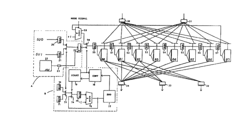
Fig. 8 shows the configuration of the main part of
a vector register of the present invention. It will be
understood that the portion encircled by a broken line A cor-
responds to the vector instruction unit Vi in Fig. 2(b), and
the portion encircled by a broken line B corresponds to the
-- i 1 32q656
25307-218
circuit of Fig. 7. The remaining part corresponds to the vector
generator shown in Fig. 5 and banks. 78 is an instruction con~
trol circuit (CONT) which discriminates whether the process
during a time slot is still in operation or it is already
finished. The instruction control circuit (CONT) 78 also
controls the steps of the process, such as write in or read out
and so on. Such steps are all similar ones which are performed
in all of the vectcr registers, and are not explicitly relevant
to the present invention. So, further description is omitted
for the sake of simplicity. 79 is a start condition detector
circuit (START) which checks all cf the isntructions waiting
for the start at the time slot, whether they cause a conflict
or not with the instruction which is now under operation, and
decides to let them start in the next time slot or let them
s art in a time slot pipe which is now idle. By a start
signal generated from the start condition detector 79, new
address and new vector length are set respectively to the multi-
plexer 58 and the selector 74, and a new vector access process
is started. The circuit relevant to such operation is also
conventional in all of the vector registers, so, further des-
cription of circuit configuration and its operation is omitted
for the sake of simplicity.
In the above disclosure of the present invention,
the embodiments described were mainly related to a vector
register having 8 banks, and each bank having 256 addresses,
for the sake of simplicity and easy understanding. The
i
- 29 -
~'
1 329656
25307-218
presently disclosed embodiments are, therefore, to be con-
sidered in all respects as illustrative and not restrictive,
the scope of the invention being indicated by the appended
claims, rather than the foregoing description, and all changes
which come within the meaning and range of equivalence of the
claims are, therefore, to be embraced therein.
- 30-