Note: Descriptions are shown in the official language in which they were submitted.
13297~8
BACKGROUND OF THE INVENTION
1 This invention relates to a process for coating one or
both surfaces of a polyimide sheet with electrolessly
deposited nickel or cobalt and electrolytically deposited
copper, to the laminate products obtained by the process and
to the textured polyimide which forms the base layer for the
; laminates.
BRIEF DESCRIPTION OF THE DRAWINGS
Figure 1 shows the embodiment of this invention coated
on one side with nickel and copper.
Figure 2 shows the embodiment of this invention coated
on both sideæ with nickel and on only one side with copper.
Figure 3 shows the embodiment of this invention coated
on both sides with nickel and coE~per.
Figure 4 shows a typical Tape Automated Bonded circuit
produceable by the process of this invention.
Figure 5 is a photomicrograph, at 65X magnification,
contrasting the textured film made by the method of this
~ invention on the right half of the photomicrograph as
; compared to film treated by the method of DeAngelo on the
left half of the photomicrograph as outlined in Example 3 of
this application. (Texturant D vs. Texturant B)
Figure 6 is a photomicrograph, at 65X magnification,
contrasting th~ textured film made by method of this
invention on the right half of the photomicrograph as
compared to film treated by the method of Redmond on the
left half of the photomicrograph as outlined in Example 12
of this application. (Texturant D of Example 3 vs. Example
12)
.
... .
132~78~
1 Figure 7 is a photomicrograph, at 65X magnification,
contrasting the textured film made by the method of this
invention on the right half of the photomicrograph as
compared to
(2a)
~ .
:
,, ,... , :: ' : '
~32978~
film treated by the modified method of DeAngelo twhere potassium
hydroxide is substituted for sodium hydroxide) on the left half
of the photomicrograph as outlined in Example 3 of this
application.(Texturant A vs. Texturant C)
Figure 8 is a photomicrograph at 65X magnification of un-
treated Type 200VM Kapton brand polyimide film which was utilized
in Examples 3 and 12 of this application.
Certain electronic assemblies have conductor traces -on both
sides of a dielectric substrate. Preferred dielectrics for ap-
plications requiring flexible substrates, especially in multi-
layer constructions, involve the use of polyimide films. In
general practice the conductive ~ayers on this substrate are
provided through the use of metal foils and adhesives specially
formulated for their physical and thermal stability. The conduc-
tive layers are also provided in some cases through direct metal-
ization by sputtering or by electroless deposition involving
methods well known to those versed in the art.
; Currently their are no commercially available polyimide lam-
inate materials, produced in the absence of an adhesive, suitable
for IPC Class 3 electronic circuit applications. The adhesive
bonding method has certain disadvantages especially in critical
service and multilayer applications, where either properties of
the adhesive or the physical space occupied by the adhesive are
limiting factors. For example, these adhesive-bonded laminate
materials exhibit poor dimensional stability, a severe
disadvantage for laying up mul~ilayer boards. The preferred
construction (especially in multilayer applications) would avoid
.. . ..
the use of adhesives and provide the metal directly bonded to the
substrate. Until the present invention, however, the methods
available for direct metalization of polyimide film substrates
had more significant drawbacks than the adhesive bonding methods.
* Trade Mark
( ~ )
.
1~29~88 ~ '
I~o methods for preparing polyimide adhesiveless metal coated
laminates are the related methods of vacuum and sputter depos-
ition, followed by electrolytic copper buildup to desired thick-
nesses. Sputtering provides better adhesion than vapor depos-
ition, but neither technique provides physical properties
adequate for critical service applications. Several commercially
available single-sided materials are produced by these methods.
The adhesion values obtained on subsequent copper buildup to
greater than 25~m are very low for materials with sputtered
copper. One structure has an initial chromium layer sputtered to
the polyimide film which is then covered with a sputtered layer
of copper. A disadvantage of this construction is that chromium
is not removed during subtractive processing of electrunic traces
using standard etchants designed to remove copper.
An alternative method for preparing a polyimide adhesiveless
metal clad laminate is to cast a liquid solution of a polyamic
acid onto the surface of a metal foil, and then to heat th~ en-
tire composition to a temperature which will imidize ~he polyamic
~ acid and form a polyimlde or amide modified polyimide film. Sev-
eral modifications of this basic technique are disclosed in
U.S~ Patents 3,682,96Q; 4,148,969; and 4,496,794. At present,
laminates produced by this techni~ue have limited application
areas due to their poor dimensional stability. This method is
also limited by the availability of suitable foil thicknesses.
In order to provide an adherent metal la~er or layers to a
polyimide film substrate by chemical metal deposition, several
basic procedures are employed. Since processing is done in aque-
ous solutions, the surface of the polyimide film must be rendered
hydrophilic to facilitate uniform adsorption of the catalyst used !i~
` 30 for seeding the electroless metal deposition. Commoniy referred ;
~.
(O
I !
,. l I
13297~ ~3
to as ~tching, this tre~tment also serves to microetch the sur- ¦
face of the polyimide, thus providing a mechanical interlock be-¦
tween the polyimide and metal layer. This surface preparative
~ step will be referred to herein as texturing for purposes of this
;,5 application to avoid confusion with the removal of unwanted metal¦
¦ during circuit preparation whiCh also is referred to as etching¦
¦ in the printed circuit industry.
I ,U.S. Patents 3,791,848 and 3,821,016 to DeAngelo disclose an
:~ aqueous ethylenediamine composition wherein the diamine is'
present in an amoUnt in excess of its degree of solubility,l
thereby forming a two-phase system. The preferred aqueous basic
compounds are disclosed as the hydroxides of the alkali metals
including sodium, potassium, lithium, rubidium, and cesium. The
examples are specif ically directed to texturing with sodiuml
hydroxide in very strong solution containing the ethylenediamine ¦
~ in suspension so as to yield a pitted surface on the polyimide.
i Since a two-phase system is utilized, the polyimide surface tends
to be non-uniformly and incompletely textured. The degree of'~
j texturing for a given portion of the surface depends upon which'
¦ phase of the solution a portion of the surface is primarily;
I ~ exposed. These non-uniformities result in subsequent non-uniforml
deposition of catalyst and electroless metal and in a rough
irregular appearance of the final metal coated film.
¦U.S. Patent 3,767,538 to Polityc~i et al, describes an attempt
to produce a well-adherent double-sided laminate on polyimide
film. The film surface is rouyhened by a fresh mixture of ¦
sulfuric and hydrochloric acids or by mechanical impingement of
sand on the surface and, if needed, a further sodium hydroxide
treatment may be employed. The polyimide film is then heated tol
¦ expel ~ater then seeded for m2talization in a colloidal palladium;
1.
~, (O
132978g
bath . Af ter thiS, an electrically conductive, water-vapor perme-
able continuous layer of silver is deposited by electroless dep-
; osition and the film is heated at 150C to expel water. Finally,
a layer of copper is electrolytically deposited to form the
laminate structUre. No specific adhesion values are reported for
the laminate produced by this method.
A high speed additive circuit process on a polyimide sub-¦
strate using electroless nickel for metalization ( no etching of I
metal reguired) is described in U . s . Patent 3, 573, 973 to Drotar¦
et al. The basic process steps are: preparing the substrate,
catalyzing, printing a mask, heat setting of the masking ink,
electroless plating of a nickel/phosphorous alloy, heating at
195C to improve metal to polyimide bond and then either
` electrolytic plating or solder coating to decrease the electrical
resistance of the resultant structure . The use Of a nickel/ j
, phosphorous alloy as-the metalizing layer may cause difficulty
~; etching laminates produced by this method during subtractive
: circuit production methods. Another disadvantage of this process
' is the need for two heating steps, the second of which is at a
very high temperature (195C) in order to provide the desired
adhesion characteristics. The adhesion values xeported are
5 . O lb. /in. maXimum by a nonstandard test and there is no mention
of the stability of the product to solder f loat . The low adhe-
. sion of metal to polyimide limits the use of these laminates to
specialty applications. The method of Drotar, therefore, does¦
not provide a method for preparation of metal coated laminates¦
for general use in the printed circuit industry.
In U . S . Patent 3, 954, 570 to Shirk et al, another additive
method is disclosed wherein the electroless deposit may be
nickel. The authors cite no advantage Of one metal over another
ll
(6)
1.
I I
~3297~8 -1 ~
n the initial metalizing step, and specifically claim a~
patterned flame sensitized surface which is catalyzed, preferablyl
With tin and palladium, then electroless plated with either cop-¦
per, nickel, or cobalt. The method of Shirk also provides low¦
bond strengths, and for the nonstandard solder dip test dis-
closed, no advantage is stated for the use of electroless nickel
rather than electroless copper or cobalt.
oAnother additive method for circUit preparation on a polyimide
substrate is disclosed in U.S. Patent 4,078,096 to Redmond et al.
I The method-described iS for teXturing the surface of the polymer
with a hydrazine/caustic solution, catalyzing, then plating with
¦ either electroless nickel, copper or cobalt. The method relates
to the preparation of a specific circuit type by an additive
process, and the maximum initial peel strength disclosed is only
~15 4.6 lb./in. Which is too low for general use in the printed~
circuit industry. Samples made by the method of this patent
result in cohesive failuxe of the polyimide film at bond values
of only 4.0 lb./in. USing the optimum formulation of 60 percen~
hydrazine hydrate and 9.3 percent sodium hydroxide disclosed by
`20 Redmond in Table II. This lowering of the cohesive strength of
the film is alluded to by Redmond in Column 4, lines 37-40, where
¦ the failure mode of well adhered and poorly adhered samples is~
~¦ discussed. Cohesive failure at suCh low values indicates
degradation of the polymer film which is seen as ripping in the
Z-axis during peel testing. There iS no disclosure of completely
coating one or both surfaces of a polyimide sheet with electro-
lessly deposited metal followed by electrolytically deposited¦
metal.
There have been prior attempts to provide an adherent metal
¦ layer on both sides of polyimide sheets by direct metalization
:
~ (7)
, I '
1329788 - ~
using electroless copper followed by electrolytic copper build-
. up to the desired thickness. This technique has proven unsuit-
able in practice SinCe blis~ering of the electroless copper layer
usually ocCurs when simultanesusly applied to both sides of the
5film. If blistering is avoided, the peel strength of the result-
ant laminate is less than that for a single-sided laminate of the
same metal thickness.
Perrins, in Transactions of the Institute of Metal Finishinq
(1972) Volume 50, pp. 38-45, discloses a process for electro-
10platin~ propylene polymers with electroless nickel or copper
¦ followed by electrolytic plating with copper. The plating in
this Case iS conducted on only one side of propylene copolymer
plaques. The use of the nickel provides improved adhesion,
especially after thermal cycling of the sample which will cause
~5degradation of the copper bond. This process, where nickel is
used as the base metal layer, has only been applied to injection
,
" molded or bulk processed polymers, but has not been extended for
use on thin film substrates. Therefore, the nickel process has
~ been restricted to use where the nickel layer is never removed
'~ 20bUt remainS a permanent part of the finished- article.
;~ In "Applications of Additive Circuitry", a Technical paper
presented at the Institute of Printed Circuits in September 1974,
Brewer discloses a method in which nickel is deposited on both
, surfaces of a paper reinforced phenolic. Electroless copper is
25then deposi~ed and the plated panel iS heated beyond the glass
transition temperature of the substrate material to improve the
~; ¦ nickel to polymer adhesion. This method is not applicable to
¦ non-thermoplastic substrates such as polyimide films.
~ Platinq and Surface Finishing, "Interfacial Bonding of Nickel
30to Polyamide-Imide", Vol.66, No. 6, (June, 1979) pp. 68-71, Levy;
(8)
~ 13 2 9 7 8 8
¦ et al, describes nickel plating on a rigid polyamide-imide sub-¦
strate textured with an abrasive and/or sodium or potassiuml
¦¦ hydroxide. The article relates the effect of various surface
~I treatments on metal adhesion, and specifically to the combi
I nation of mechanical abrasion followed by a chemical treatment
such as dipping in agueous alkali metal hydroxide solutLons. The
article states that no advantage was observed with the use of
nickel rather than copper for the initial m~talization of the~
polymer, and concludes that the adhesion of the metal to thei
polyamideimide substrate is a combination of both mechanical and¦
chemical factors related to the substrate.
Prior to the present invention, thexe has been no commer-
cially viable method available for the direct coating of poly-
imide films with ~lectrically conductive layers, without the use¦
` 15 of an adhesive, exhibiting adequate properties ~or general use in
~ electronic circuitry. No adhesiveless laminates with metal on
.. I
both sides have been available due to the tendency for an elec-
troless metal layer to blister during deposition onto both sides
of a thin film, and to the destruction of polyimide to met~l
adhesion by thermal shock upon immersion in molten solder or
because of undesirable reduction of film strenyth due to textur-
ing. The problem of electroless metal blistering is especially¦
acute in the complete metalization of thin polymeric film; hydro-¦
¦ gen evolution during the deposition process has been suggested as¦
a cause of electroless metal blistering. Electroless metal¦
blistering on thin polymeric substrates is greatly reduced when
the metal deposition is restricted to certain areas on the film
(i.e. other than complete surface coverage).
It would be desirable to provide a process for coating atj
least one surface of a ~olyimide film with electrolessly depo-¦
11 (9)
.
~ 132978~ .
sited metal, followed by electrolytically deposited copper having
sufficient adherent strength to the polyimide and sufficient
resistance to thermal shock to render the resultant laminate
useful for fabricating electronic circuits.
SU~MARY OF THE INVENTION
The present invention is directed to a process whereby a
polyimide sheet or continuous web of uniformly and completely
textured polyimide film is uniformly coated on one or both
surfaces-with a strongly adherent electroless nickel or cobalt
layer followed by an electrolytic copper layer. Adherent layers
of exposed copper are uniformly plated on one or both sides of
the sheet and metal layers of controlled thickness are produced
which provide laminates useful for the production of electronic
circuitry. These laminate structures are suitable for general
use in the production of electroni.c Circuitry. The terms "web",
"sheet" and "~ilm" are used herein interchangeably and refer to
thin f lat polymer substrates.
¦ In accordance With the present invention, there is provided a
¦ process for forming an adherent exposed copper coating on the
:! surf aces of a polyimide sheet or f ilm sUch as the type prepared
.~ f rom the anhydride of pyromellitic acid and 4,4'-diamino-diphenyl
ether. At least one surface of a polyimide sheet is first treat-
ed with a one-phase solution of an alkali metal hydxoxide, an
alcohol and a diamine of the formula H2N(CH2)nNH2 wherein n iS an
integer from 2 to 6, preferably ethylenediamine, to provide a
textured and hydrophilic surface, where a uniformly and com-
pletely textured suxface of a particular topography is produced
and the mechanical bulk properties of the film are substantially
unaffected. The surface of the textured film is characterized by
(lO)
~ 13297~8 - ~
nodules or bumps, rather than pits as reported for other
texturing metho~s. When viewed through a microscope the comp-
leteness of surface texturing is readily seen. Photomicrographs
of the film textured by the methods of U.S. Patents 3,791,848
and 4,078,096 to DeAngelo and Redmond respectively, are shown
compared to the film textured by the method of this invention in
Figures S,6 and 7. The substantially complete texturing produced¦
by this method can be seen by the more pronounced and uniform¦
~; scattering of the light, as compared to the film produced by¦
either of~ the other methods which are darker in appearance and¦
therefore not as completely textured.
The surface of the film is rendered uniformly frosted and
matte with a translucent appearance so that a surface receptivel
to colloidal catalyzation and the subse~uent electroless deposi-¦
I tion of an electrically conductive metal layer is provided, yet
; ¦ the original mechnical bulk properties of the film are substanti-
¦ ally unaffected. The resulting uniformly and completely textured
¦ surface of the polyimide film lS contacted with colloidal pal-
; ¦ ladium in order to provide a catalytic surface for the deposition
of electroless nickel or cobalt. Nickel or cobalt is then depos-
ited on the receptive surfaces by electroless deposition to form
a hydrogen gas and water vapor permeable layer which is elec-
trically conductive. No high temperature baking of the film is
¦ necessary before the step of electrolytic buildup with copper.
1 25 ¦ As used herein, the term "nickel", as it relates to the initial
metal layer, includes nickel metal or a nickel containing alloy.
Also as used herein, the term "cobalt", as it relates to the
¦ initial metal layer includes cobalt metal or a cobalt containing
l alloy. This textured film can also be useful as a substrate for
the fabrication of adhesive-based metal clad laminates.
~.~ i .'
(ll)
~ 132!17~8
In accordance with this invention, laminate constructions are
provided which are coated on one surface with electroless
deposited nickel or cobalt and electrolytically deposited copper,
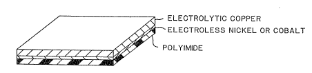
the second surface being either bare polyimide ~Fig. 1) or coated
with electroless nickel or cohalt (Fig. 2). When tested accord-
ing to IPC test 2.4.9 (July 1985 update), these laminates are
characterized by peel strengths of at least 6.0 lb./in. and usu-
ally greater than about 7.0 lb./in. by Method A and 4.5 lb./in.¦
by Method C. These laminates also pass IPC tes~ 2.4.13 (December¦
- 10 1982 update). All test methods referred to herein are from IPC
TM 650, and are performed using laminates that have been coated
with metal to a thickness of 35~m. These are test methods
normally used by circuit manufacturers to determine laminate mat-
erial ~uality. When the electroless nickel or cobalt thickness
is greater than about l.O~m with either of these two construc-
tions, adhesion values of at least 5.0 lb./in. and usually great-
er than 6.0 lb./inO can be obtained with IPC test 2.4.9,
Method C. The double-sided const:ruction passes a more riqorous
modification of IPC test 2.4.13 where metal remains on both sides
of the sample. Prior to this present invention, no double-sided
; laminate, apart ~rom adhesive-based laminates, were capable of
passing this more stringent test.
The textured film produced by the texturant outlined above,
and the subsequent use of nickel or cobalt metalization in a
~ unique two-step sequence, yields a superior laminate. The combi-
; nation of these two steps unexpectedly provides enhanced solder
float resistance, which is not obtained by the use of nickel
metalization alone, as shown in Example 3 of this application.
1 32978~
1 In one aspect, the present invention resides in a
process for coating at Ieast one surface of a polyimide
sheet with copper in the absence of an adhesive, said
process comprising contacting said sheet with a one-phase
solution comprising about 3 to 15 percent by weight of a
diamine with the formula H2N(CH2)~NH2 wherein n is an
- integer between 2 and 6, between about 15-40 percent by
.: weight of an alkali metal hydroxide, between about 10 and 40
percent by weight of a water miscible alcohol and the
remainder of the solution water, for a time and at a
; temperature sufficient to render said surface uniformly and
substantially completely textured, treating said surface
:-: with a catalyst to create a surface receptive to the
electroless deposition of nick~l or cobalt, depositing a
~. 15 nickel or cobalt metal layer on said receptive surface by
: electroless deposition to form a nickel or cobalt coatPd
surface of said sheet, said deposited nickel or cobalt metal
layer being electrically conductive, and depositing copp~r
on said nickel or cobalt metal layer by electrolytic
deposition to form at least one exposed copper coating on
said polyimide sheet.
In another aspect, the present invention resides in a
polyimide laminate sheet product including as one layer of
said laminate sheet product a polyimide sheet having two
surfaces, each of sa.id polyimide sheet surfaces being
: (12a)
~ .
. . ,
~329788
] uniformly and substantially completely textured and each of
said polyimide sheet surfaces being free of an adhesive and
having a metal coating comprising an electroless nickel or
cobalt coating and and electrolytic copper coating bonded to
~` 5 each of said nickel or cobalt coatings, said laminate sheet
product having a peel strength of at least 6.0 lb.jin. as
measured by IPC Test 2.4.9 Method A and a peel strength of
at least 4.5 lb./in. as measured by IPC Test 2.4.9 Method C
and being capable of passing IPC Test 2.4.13 for solder
; lO float.
In a further aspect, the present invention resides in a
polyimide laminate sheet product including as one layer of
said laminate sheet product a polyimide sheet having two
sur~aces, at least one of said polyimide sheet surfaces
being uniformly and substantially completely textured and
one of said polyimide sheet surfaces being uncoated or being
uniformly and substantially completely textured and coated
with an electroless nickel or cobalt coating, a second
surface of said polyimide sheet being uniformly and
substantially completely textured and coated with an
electroless nickel or cobalt coating directly on said second
surface and an electrolytic copper coating on said nickel or
cobalt coating, each of said polyimide sheet surfaces coated
with a metal being free of an adhesive; the coating on said
(12b)
~' ,
,,~
.
: ~3%97~
1 s~cond surface having a peel strength of at least 6.0
lb./in. as measured by IPC Test 2.4.9 Method A and a peel
: strPngth of at least 4.5 lb./in. as measured by IPC Test
2.4.9 Method C and being capable of passing the IPC Test
2.4.13 for sclder float.
,.,
.~ 15
;:
;:~
.
. 25
~; (12c)
., ,, ,~.. ..
'' ' ~ "
,
13297~
In another aspect of this invention, a laminate construction
is provided which is coated on both surfaces with electroless
nickel or cobalt and electrolytic copper ~Fig. 3), and has a peel
strength of at least 6.0 lb./in. and usually greater than
7.0 lb./in. by IPC test 2.4.9t Method A, and at least 4.5 lb./
in. by IPC test 2.4.9, Method C. When the electroless nickel or
cobalt thickness is greater than about l.O~m on this double-sided
laminate construction, adhesion values are greater ~han
6.0 lb./in. by IPC test 2.4.9, Method C.
~n DESCRIPTION OF THE SPECIFIC EMBODIMENTS
In the preferred embodiment of this invention, the polyimide
surfaces treated are of the type prepared from a polyamide-acid
(also referred to as polyamic acid) which has the formula:
~OOC~ ~COO~ 1
_ - N-C ~ C-N-R' --
H 0 0 H n
where the arrows denote isomerism, R is an organic tetravalent
radical containing at least two carbon atoms, no more than two
carbonyl groups of each polyamic acid unit being attached to any
onP carbon atom of said tetravalent radical; R' is a divalent
radical containing at least two carbon atoms, the amide groups of
adjacent polyamide-acid units attached to separate carbon atoms
of divalent radical and n is a positive integer sufficient to
provide the polyamic acid with an inherent viscosity of at least
; (13)
:~.
11 ~3297~8
..
0.1. The most preferred of such polyimides is Kapton (Trademark
registered to ~uPont) which is the polyimide formed from
pyromellitic ~nhydride,
;.and 4,4'-diamino-diphenyl ether,
', 10
H2N~--o ~NH2
and having the general formula:
15 l _ o ~ ,.
--- ~ Cl)~f/ ~ ~3--~
I where n is an integer ranging from 150 to 650 and which has an
¦ average molecular weight of 60,000 to 250,000. The above
polyimides and ~heir preparation are described in U.S. Patents
3,179,614 and 3,179,634 to Edwards.
The polyimide can have any thickness suitable as a substrate
¦ for electronic circuitry, and most generally is in the form of a
¦ relatively thin sheet having a thickness of between about 12 and
¦1 125~m. Prior to this invention, a polyimide film coated on both
sides with a permanently bonded metal comprising electroless
~,nickel followed by electrolytic copper capable of passing current
.i(14)
.,, .
, !!
132~788
~¦. ~ IPC tests, in particular IPC tests 2.4.9 and 2.4.13, for adhesion
and thermal shock, has not been achieved without the use of a¦
~ separate adhesive layer. Although the preferred embodiment ofl
i~ this invention relates to the polyimide film described above, it¦
S is understood that with the surface preparation step of this¦
~ invention, thin fllms produced by other modifications of a basic
., . polyimide structure can also provide useful laminates when
~ processed in accordance with the method disclosed herein.
;;, . This invention also relates to a method for coating one orl
! both sides of the textured polyimide sheet (web, film) with well
adherent metal layers. These metal layers when applied according
to the method disclosed herein are suitable for use in electronic
circuitry, especially in applications where the use of an adhe-
sive would be detrimental to the performance or construction of .
. the final product. Once the metal layers are provided as dis-
~ closed, they can be further processed through means normally em
; ployed in the electronics industry, and lend themselves to both
semi-addltive and subtractive methods to form one or two¦
patterned layers for circuit preparation as summarized in the
~ follo~in ~utline:
,,' . ' .
(15)
ll 1 329788
; ~ Methods Used for Circuit Preparation
~;~ Semi-additive Process Subtractive Process _
;:~.
~ Thin Laminate Thick Laminate
;~ 5 (e.g., 0.5-8um metal) (e.g., 3Sum metal)
Resist coat Resist coat
¦ Photoimage Photoimage
Develop resist Develop resist
Electrolytic copper plate Etch unmasked metal
(e.g., 35um)
Strip resist Strip resist
, I Etch to remove thin lami-
nate metals
I No modification of existing procedures for the production of
15 ¦ said circuitry is necessary using laminates of this invention. A
jj further advantage for the use of the method of this invention is
~, I that metal thicknesses can be provided easily from extremely thin
to very thick layersD Laminates with layers of metal less than
about 18um (1/2 ounce) are difficult to produce using present ad-
20hesive laminate production methods, but are easily produced in a
continuous roll-to-roll process by the method of this invention.
The polyimide ~ilm surface should be relatively clean, but a
cleaning or degreasing s~ep may be performed (if necessary) prior
¦to contact with a suitable texturant. The textur~nt of this
25invention provides a uniformly and completely frosted or matte
. appearance to the surface of the film which is due to nodules
`~ remaining when surrounding material is selectively dissolved by
,~the texturant. The one-phase texturing compo~ition
(16)
13297~g
; is comprised of an alkali metal hydroxide, a diamine of the form-
ula H2N(CH2)nNH2 wherein n is an integer from 2 to 6, preferably
ethylenediamine, and a water miscible alcohol such as methanol,
ethanol, isopropanol or n-propanol. The alkali metal hydroxide
can comprise potassium hydroxide, sodium hydroxide, lithium hy-
droxide or mixtures thereof, with potassium hydroxide being pre-
¦ ferred. In addition, quaternary ammonium hydroxides such as tet-
; ramethylammonium hydroxide, can be used. The concentration of
the diamine in the texturing solution is sufficient to effect the
desired surface modification without forming a two phase liquid
composi~ion and is between about 3 and 15 percent by weight.
Suitable compositions range between 15 and 40 percent by weight
¦ alkali metal hydroxide, 3 to 15 percent by weight diamine, and 10
to 50 percent by weight of an alcohol or mixture of alcohols one
of whose functions is to act as a cosolvent and provide a one-
phase solution; the balance of the mixture is water. The parti-
cular percentage of each component in the texturant is adjusted
according to the content of alkali hydroxide or diamine in order
to maintain a one-phase system at the temperature used for
texturing the film. As set forth above, the textured film of
this invention is uniformly and completely textured.
Once the cl~an polyimide surface has been treated to render
the surface hydrophilic, the film is catalyzed with any one of
the catalyst systems well known to those versed in the art of
electroless plating. Catalyst combinations which can be used in
conjunction with the sensitized polyimide surface are disclosed
in U.S. Patents 3,011,920 and 3,562,038. The catalyst may be
applied in a two step application, by first depositing the
sensitizer and then the noble metal activator; however,
these baths may be combined in
tl7~
~ 32978~
` ~
1 noble metal activator; however, these baths may be combined ir. a
one s~ep operation, e.g. a black colored tin-palladium colloidal
dispersion. The catalyzing is provided for a period of one to
five minutes, and then the sample is imme~sed in an acidic
solution to remove tin from the surface in a process referred to
as acceleration. The sample is then placed in an electroless
nickel or cobalt bath for a period rangin~ from about ~wo ~o ten
minutes to provide the desired thickness of nickel.
Suitable electroless nickel baths are disclosed in U.S.
Patents 3,062,666; 3,140,188; 3,338,726; 3,531,301: 3,537,878;
and 3,562,038. ~:ome typical formulations are shown:
1. Nickel chloride (NiCl2~6H20) 20.0 g/l
Sodium hypophosphite (NaH2PO2~H20) 60.0 g/l
Ammonium oxalate ~(NH4)2C2O4-H2O) 40.0 g/l
Ammonium ~ydroxide 25% 60.0 ml/}
pH 8.2, 85C
2. Wickel Sulphate (NiSO4-6H20) 17.1 g/l
Sodiwm Hypophosphite (NaH2PO2-H2O) 14.0 g/l
.~ Acetic Acid 80% 12.0 g/l
~, 20 MoO3 85%1adjust to control rate) S.0 mg/l
p~ 5.2-5.5, 95~
.
.
. .
''
(18)
132~7~ I
3. Nickel Sulfate (NiSO4-6H20) 20.0 g/l
Dimethylamine Borane 3.0 g/1
Citric Acid 10.0 g/l
l Conc. HCl 25.0 ml/l
;~ Ammonium Hydroxide to pH 7.0
2-Mercaptobenzothiazole 0.5-2.0 mg/1
65C
- 4. Nickel Chloride (NiC12-6H20) 16.0 g/l
; 10 Dimethylamine Borane 3.0 g/l
Sodium Citrate 18.0 g/l
~lycine 8.0 g/l
Bismuth Nitrate 20.0 mg/l
Thiourea 15.0 mg/l
j15 pH 7.0, 65C
': .,
Nickel or cobalt is deposited on the receptive surfaces by
electroless deposition to form a metal coated surface. Nickel
ions are reduced in this process onto the catalytic surface to
form a continuous electrically conductive layer. The electroless¦
layer must be suffi~ciently thick to permit the subsequentl
electrolytic deposition of a uniform copper layer. Generally the¦
~' electroless nickel or cobalt layer is between about 0.25~m and
1.O~m thick but can be thicker if desired. No substantial~
, 25 advantages are obtained with nickel or cobalt coatings greater~
than about l.O~m. j
The use of nickel or cobalt rather than copper as an initialj
metal layer provides several significant advantages. In the
electroless deposition of metal, a certain amount of hydrogen gas
is liberated as part of the reaction. Hydrogen gas is gener-
!
(19)
'."
.,
''
~ ' ' , .
1~2978~ ~ .
ally considered a cause of blistering during electroless copper
- deposition, and blistering has been a problem associated withl
production of a double-sided laminate on polyimide films when~
electroless copper is used for initial metalization. When elec-¦
S troless nickel or cobalt is substituted for electroless copper,~
especially nickel or cobalt deposited from a borane reduced bath,
the blistering is alleviated. Unexpectedly, it has been found
that electroless nickel/boron alloys etch more easily than elec-
troless nickel/phosphorous alloys when standard copper etchants
such as cupric chloride are used. The nickel/boron alloy pro-
ducing baths are easier to use with a continuous reel to reel¦
- process and are not as prone to catastrophic decomposition as are¦
nickel/phosphorous alloy producing baths. These nickel/boron~
baths also are characterized by a greater number of metal turn-
overs which provides longer service life in continuous operation
than nickel/ phosphorous baths. It is preferred to utilize elec-
troless nickel baths wherein the reducer for the nickel is
dimethylamine borane (DMAB), since the resultant nickel coating
can be subsequently etched with a comm~n etching solution such as
i 20 copper chloride. Electroless cobalt can also be deposited from al
bath formulation using DMAB as a reducer and may find use as anl
initial metal layer. Copper and palladium are not useful asl
, ~ initial metal layers since they can catalyze degradation of the
polyimide and lead to poor post solder float peel strength values
due to thermal sensitivity of the final laminate structure.
A serious deficiency of prior adhesiveless laminates when
~3 compared to their adhesive-based count~rparts is their failure
when subjected to standard testing for thermal shock by
IPC test 2.4.9 Method C. This thermal shock failure is
characterized by catastrophic loss of bond strength after solder
,~, ~ ' I
i (20)
~; ~ 132g78~ ~
float. The laminates made f rom the presen~ invention have super-
ior performance when compared to presently available single-
sided adhesiveless laminate structures. When tested for metal to
substrate adhesion after solder float as per IPC test 2.4.9,
Method C; adhesion in the 4 . 5 to 5 . 0 lb. /in~ range is typical.
With thicker nickel metalization, values greater than 6.0 lb./in.
can be obtained. When copper is used as the electroless
metalizing layer rather than nickel on single-sided laminate
structures, post solder float values are usually less than
3.0 lb./in., and total metal delamination (blowoff) is common.
The method of this invention provides the only single- or
double-sided adhesiveless laminates Which provide products that
pass solder float adhesion testing by IPC test 2.4.9 Method C.
The combination of proper polyimide film pretreatment and
lS electroless bath chemistry, has provided an adhesiveless laminate
superior to those presently available. A laminate with these
particular properties has not h~retofore been available. In
particular, this invention provides a laminate with the following
advantages over the prior art:
' 20 1. Single or double-sided adhesiveless laminate con-
i structions with excellent adhesion.
2. Initial adhesion values superior to those obtained
using electroless copper for both single- and double-sided
~ laminate constructions.
I 25 3. Post solder float adhesion greater than that ob-¦
tained by other methods, with no random failure or blowoff during¦
;~ solder float testing as per IPC test 2.4.9 or 2 . 4 .13 .
..
',.
,~' .'
~. (21)
l ~32g78.~
4. No high temperature drying needed between electro-
less and electrolytic plating steps, thus providing more rapid
processing times.
5. A superior laminate provided consistently with both
sheet and roll-to-roll processing of the film.
6. Laminate structures can be provided having very thin
conductive layers produced at significant cost savings, and more
reliably than those produced by prior methods.
7> Laminate structures with improved flex ductility when
compared to the adhesive-~ased and adhesiveless laminates
presently available.
8. Laminate structures which have improved dimensional
stability when compared to adhesive-based laminates.
9. Metal coated laminates processable under conditions
, 15 normally utilized for production of circuitry when a nickel/boron
alloy is used for initial metalizatlon.
, The following examples illustrate the present invention and
are not intented to limit the same.
., .
EXAMPLE 1
A four inch by six inch sample of type VN200 Kapton brand
polyimide film is treated to render the surface hydrophilic and
textured with an aqueous alkali metal hydroxide, methanol and
ethylenediamine composition. The texturing composition is com-
prised of 37.4 percent by weight po~assium hydroxide, 10 percent
by weight methànol, and 7.0 percent by weight ethylenediamine
EDA) in an aqueous solutio~. Total film thickness is reduced
l from 48 to 41~m in the texturing process and the film has a uni-
i formly and completely frosted appearance. This treated film is
~ 30 further ocessed on both surfaoes with the lollowing sequence:
'.'' . ,
. .
,.,
ll 132~7~8 ~ I
1. 60 sec. at 25C in 23% solution of an aqueous acid
bath sold under the tradename, Shipley Cataprep* 404 available
from Shipley Corp.
2. 120 sec. at 45C in a 3% concentration of an aqueous
S colloidal palladium catalyst sold under the tradename, Shipley
Cataposit* 44 available from Shipley Corp.
3. Rinse for 60 sec. in water
~ 4. 180 sec. at 25C in a 10% solution of an acidic
;~ accelerator sold under the tradename, Shipley Accelerator 19
available from Shipley Corp.
5. Rinse for 30 sec. in water.
6. 120 sec. at 65C in an electroless nickel plating
l solution, utilizing dimethylamine borane as the reducing agent,
: sold under the tradename Niklad* 752 from the Allied Kelite
division of Witco Chemical Corp. Final nickel thickness approxi-
; $ mates 0 . 5~m.
7. 90 minutes at 15 amps per square foot (ASF) in a
brightened copper sulfate bath containing 25 ounces per gallon of
sulfuric acid, 15 ounces per gallon of copper sulfate pentahy-
,~ 20 drate, 50-70 ppm chloride ionl ancl 1.0% of an organic brigh~ener;; . sold under the tradename, Copperlume*PTH-R from M&T Chemicals Co.
This provides a laminate coated with about 35~m of copper.
This sample which has been coated on both sides with
electroless nickel followed by electrolytically deposited copper
is then dried at 80C for 30 minutes. After masking with
chemically resistant tape, 1/8th inch lines are revealed using a
copper chloride e~ching solution to remove metal from unmasked~
.~ areas of the sample. The tape is removed, the sample is dried,
and then an Instron*Model 1000 Universal Testing Instrument is
*Trade Mark
''''j
. ~23)
,
. l I
. I . ~ ~
~. . . . .. i
~l ~32g7~ `` ~
used to perform 90 degree peels using IPC test 2.4.9, Method A,
Average adhesion of 10.0 lb. /in. is obtained and no side to side
variation is observed.
EXAMPLE 2
A sample of type VN200 Kapton brand polyimide film is tex-
tured and metalized by the procedure of Example 1 and plated to a
final thickness of about 35 ~m of electrolytic copper on both
sides . The approXimate nickel thickness is 0.50~m. The adhesion
of 1/8th inch lines etched from this sample is 8-9 lb. /in. The
sample is then tested for adhesion after solder f loat as per IPC
test 2.4.9, Method C. The etched lines are coated with less than
50~m of Dow Cornin~ high vacuum silicone grease, and floated for
five seconds on molten solder Which is held at 288C. No metal
blowoff is observed on the 1/8th inch traces, and the final
adhesion of ~hese heat shocked materials was 4.8 lb. /in.
~.',
. ¦ EXAMPLE 3
.- Four inch by six inch samples of type VN200 Kapton brand
polyimide film are textured by the four different compositions
shown in the following table, then catalyzed by the procedure
described in Example 1, and then metalized with either ( a) an
electroless copper bath containing formaldehyde as a reducing
agent and sold under the tradename Enduroplate*EP-407 by Hunt
Chemical Co., or ~b) the Niklad 752 electroless nickel bath
described earlier. The EP-407 bath is a low deposit electroless
copper bath whiCh has been found to provide the best results O~
copper bath formulations tested on polyimide film textured by the
~` method of thiS invention.
*Trade Mark
.
~ (24)
i
~32~788
Textur_ nt compositions
TexturantNaOH KOH EDACH30H H2O
... .. . . ~ _ _ _ I
A - * 0.0% 41.8% 7.0%0.0% 51.2%
(10.5 M)
B - **28.0% 0.0% 7.0%0.0% 65.0
~¦l (9.1 M)
C 0.0% 37.4% 7.0%10.0% 45.6%
D 27.7% 0~0% 7.0%10.0% 55.3%
* - Texturant from Example lD, U.S. Patent 3,791,848 to
DeAngelo, where 45 percent by weight potassium hy-
droxide is substituted for 10 N sodium hydroxide.
** - Texturant from Example lD, U.S. Patent 3,791,848 to
DeAngelo.
- Texturants C and D are homogeneous liquid composi-
lS tions in accordance with this invention.`
. ~
Figure 5 shows the surfaces resulting from the use of Tex-
turant D vS~ the use of Texturant B. The darker side on the leftl
of Figure 5 is the surface resulting from the use of Texturant B¦
while the lighter side on the right of Figure 5 is the surface
! resulting from the use of Texturant D. The use of Texturant D,
"~~ . I
j results in a uniform and completely treated surface. The surface;
resulting from the use of Texturant B is incompletely textured asl
shown by the large portion of the surface which iS darker. !
Figure 7 shows the surfaces resulting from the use of Texturant Al
vs. the use of Texturant C. The dar~er slde on the left of Figuxe¦
7 is the surface resulting from the use of Texturant A while the¦
, lighter side on the right of Figure 5 iS the surface resulting~
t from the use of Texturant C. The use of Texturant C results i~ a
' 30 uniform and completely treated surface. The surface resulting
:~ , . ' .
~ (25) .
I .
~"'' ..
. . .
1~2~7~8
from the use of Texturant A is incompletely textured as shown b~
the large portion of the surface which is darker. The surface~
shown in the left half of Figures 5 and 7 more closely resemble
the surface of untreated film as shown in Figure 8.
These samples are then electrolytically copper plated to a~
' final metal thickness of approximately one ounce per square foot,¦
or about 35~m. IPC test 2.4.9, Methods A and C were then per-l
formed for initial and post solder float adhesion, respectively,
with the following result:
Sample Initial Initial Peel (lb./in.) Solder Float
! No. Texturant Metal Side A Side B Peel (lb./in.)
;1- ¦ l A Ni 5.2 6.4 0 - 3
2 A Cu 4.8 4.8 Blowoff
l 3 B Ni 7.4 8,5 0 - 4
I lS 4 B Cu 6.7 8.4 Blowoff
C Nl 7.9 6.8 4.6
6 C Cu 6.5 8.0 Blowoff
7 D Ni 9.4 lO.0 4.4
8 D Cu 7.5 7.l Blowoff
`,` 20
All reported adhesion values are for peels at 90 degrees for
l/8th inch traces performed using an Instron model lO00 universal¦
! tester. An average of at least three l/8th inch traces are used
for each value shown in the table above. Two major conclusions
can be drawn from ~he lnformation presented in the table above:
l. The homogeneous texturing solution of this
. - invention such as that represented by Texturant C or D provides
overall superior solder float performance.
2. Nickel metalization provides superior post solder
float performance.
.
~ (261
~ 3297~
1 In every case the combination of either Texturant C or
D, and the use of electroless nickel provides a superior
laminate to that produced by the application of the two-
phase texturant as taught by DeAngelo.
The samples using the nickel for electroless
metalization show more consistent adhesion values which are
much higher overall than those obtained with the electroless
copper samples. There is no random blowoff on solder float
as is found for eléctroless copper metalized samples.
EXAMPLE 4
- Three samples of type VN200 Kapton brand polyimide film
are textured and metalized as in Example 1, except that they
are plated for different times with electroless nickel to
pro~ide samples of varying nickel thickness. After
electrolytic copper plating to 35~m per side in a brightened
copper sulfate bath, all three samples are solder floated as
in Example 3, with the ~ollowing results:
Sample Electroless nicXel !Niklad 752~Adhesion after
Nio. Time Thickness solder float
201 ~ minutes 0.25 ~m 3 - 4 lb./in.
2 5 minutes 0.65 ~m 4 - 5 lb./in.
3 10 minutes 1.25 ~m 6 - 7 lb./in.
This Example shows that the samples with the thicker
, nickel layers have the better post solder float adhesion.
The metal thicknesses shown in this Example are easily
achieved in the process of this present method on a reel to
reel production basis, i.e., through a process where a
continuous web of polyimide film sequentially is passed
- through the multiple steps of the process
(27)
-
' ! ' ' ' , ' . . ' : :
~ ~ ~3~7~g
ith intermediate washing steps between the adjacent pro~ess,
steps in a continuous manner.
:~ I ,
EXAMPLE 5
A 450 Eoot long, 12 inch wide, roll of type VN200 Kapton brand~
polyimide film was processed on both surfaces by the same¦
procedure used in Example 1, but in a continuous roll-to-roll
process. In order to obtain adhesion between the electroless andl
electrolytic metal layers special care is taken in the design of;
the electroplating cell to insure that the optimum current dis-
tribution is provided to the web. After electrolytic copper
bUildUp to 35~m on both surfaces in a brightened copper bath,
small representative samples were cUt from the web for testing,
and then 1/8th inch lines were revealed by tape masking and¦
etching. The initial adhesion values obtained by IPC test 2.4.9,¦
Method A averaged 9-10 lb./in. The adhesion values for these¦
samples after solder float were 5.0-5.5 lb./in., as per IPC test
2.4.9, Method C.
~.1
~,~ 20 EXAMPLE 6
! A four inch by siX inch sample of type VN200 Kapton brand
l ~ polyimide f ilm is prepared as in Example 1 up to the electroless~
;, . nickel step, bUt iS only plated on one side With electrolytic
~` copper. This selective plating is accomplished by coating one
; 25 side of the sample with a plating resist. The final laminate
structure is comprised of double-sided electroless nickel and
35~m of electrolytic copper on one side only. This sample is
sub~ected to a more rigorous test than IPC test 2.4.13, "Solder
Float Resistance - Flexible Printed Wiring Materials" wherein the
sample is tested without removing metal from either side; the
(28)
~-
1~7~8
samples are cut into two-inch squares, baked at 135+10C for one~
hour; then floated for 10 seconds on solder,held at 260+5C.
This sample suffers no blowoffs or delaminations.
. I
¦ EXAMPLE 7
A four inch by six inch sample of type VN200 Kapton brandl
polyimide film is backed on one side with tape, and textured asl
in Example 1. After pretreatment in a palladium catalyst
solution, the tape is removed, followed by electroless nickel
I buildup, and electrolytic plating to 35~m in a brightened acid¦
copper sulfate bath bY the method of Example 1. After plating,¦
1/8th inch lines are revealed using a copper chloride etchant.
After removing surface moisture at 80C for 30 minutes, one half
of the lines are peel tested fox adhesion before solder float,
the other half of the lines are subjected to a solder float, and
then peel tested as in IPC test 2.4.9, Methods A and C yielding
values of 8-9 lb./in. and 4.8 to 5.0 lb./in., respectively.
-,, EXAMPLE 8
A four inch by six inch sample of type VN200 Kapton brand~
polyimide film is textured, catalyzed and accelerated as in Exam-¦
;~ ple 1 t followed by electroless plating for two minutes ln a
hypophosphite-reduced nickel bath, product no. 139-500011-71,
obtained from the J.E. Halma Co.- This particular nickel bath
provides a low phosphorous niçkel alloy containing 3-5% phos-
phorous by weight. The sample is then plated on both sides to
about 35~m of copper in a brightened acid copper sulfate bath.
It was found that this nickel deposit had a differential etch
rate compared to the copper, but it is eventually removed cleanly
~ in the unmasked areas by the use of a copper chloride etchant.
~ ' . ,
(29)
2 9 7 ~ ~
EXAMPLE 9
This Example illustrates the usefulness of the laminates
produced by the method disclosed herein for the preparation of
circuits by the subtractive method set forth above. Laminate
S constructions are prepared on type VN200 Kapton brand polyimide
film using the procedure of Example 1 on one side of the film up
to the point of electrolytic metalization. To prevent treatment
;; of the other side of the film one side of the sample is masked
with tape, and the tape is removed just before electroless metal-¦
ization. For the preparation of a particular type of printed¦ '
circuit pattern referred to as a TAB (Tape Automated Bonding)
circuit (Fig. 4) which is used as a chip carrier for mounting
integrated circuits (chips) by the subtractive method, the copper
is only electroplated to about 17~m in a brightened copper
i15 sulfate bath.
The laminates are first cleaned for one minute at 359C in a
1.0 M NaOH solution containing a wetting agent, followed by
cleaning for 30 seconds at 25C in 1.0% agueous nitric acid,
followed by thorough wa~er rinsing and drying of the sample. The
laminates are next coated with a positive liquid photoresist
available from Shipley Corp. under the tradename Shiple~ AZ-119S~
A final dry film thickness o 5~m is obtained after drying at
80C for 30 minutes as per manufacturers instructions. A posi-
tive photoresist coating is a composition which becomes soluble
in an a~ueous developing solution on exposure to ultraviolet ( W )
light energy . The resist coated laminate is then masked with a
phototool and exposed using an ultraviolet exposure unit at 200
millijoules per square centimeter to image the TAB circuit
pattern. The exposed resist is then developed in a two stage
treatment using Shipley*303A developer from Shipley Corpc The
*Trade Mark
(30)
:',:
: I
ll I
~3297~8 ` I
! sample is immersed for two minutes in a 25% concentration of the~
dev~loper followed by 30 seconds in a 20% solution of the devel-l
oper. A clean, sharp resist image of the TAB circuit pattern is¦
obtained. The resist is then post baked to harden for one hour¦
at 125C. The exposed copper and underlying electroless nickel
I ¦ is removed in a copper chloride etchant. I
The method of this Example produces a TAB circuit as shown in
Figure 4 with clean line definition of at least 75-100 ~m.
EXAMPLE 10
This Example shows the utility of laminates produced by the
present me~hod for a typical semi-additive circuit preparation
In the semi-additive process of circuit preparation a thin layerl
of copper of up to about 8.0 ~m is plated to provide a more high-¦
ly conductive metal layer to facilitate subsequent electrolytic
deposition of copper to a final desired thickness. This initial
thin copper layer can be electrolessly or electrolytically
deposited on the nickel.
A sample of type VN200 Kapton brand polyimide film is tex-
tured and coated with electroless nickel by the procedure of
Example 1, and then electrolytically flashed to a thickness of¦
only 3~m with copper. This copper surface is then cleaned in an
alkaline degreasing solution for one minute, followed by 25% HCl
I containing 0.5% HNO3 for one minute at 25C , then water rinsed
¦ and dried. Risto~ photopolymer dry film from DuPont is then hot
~: roll laminated to the cleaned surface of the copper, and a TAB
circuit (Fig. 4) is imaged through a negative photomask with an
ultraviolet light source, and then developed using Riston
developer. Riston photopolymer dry film is a negative photo-
resist, so the areas exposed to ultraviolet (UV) light energy
; *Trade Mark
(31)
:
Il ~3297~8 1l
become insoluble in the developing solution. The TAB circuit :is~
then plated to a thickness of about 35~m in the non-masked are~s~
using a brightened copper sulfate bath. The resist is stripped,¦
and the thin copper/nic~el flash is removed in a ferric chloride
etching solution.
Good line defini~ions at 75-100~m line dimensions again are !
obtained in the finished circuit.
solutio~
" , I
EXAMPLE 11
A double-sided copper clad laminate of the type shown in~
Fig. 3 is prepared by the procedure of Example 1 and tested in~
accordance with IPC test 2.4.13 as follows:
1. One side of the sample is masked wi~h tape.
2. The metal is then removed from the unmasked side in
a copper chloride etchant, and the tape mask is removed.
3. A two inch square is cut from the specimen.
4. The sample is then placed in an oven at 135+5C for~
one hour.
~, 29 5. The surface is cleaned by the use of an acid flux.
6. The sample is floated for 10 seconds just beneath
the surface of molten solder held at 250+10C .
7. The uncoated side of the sample is then inspected !
for metal delamination and separation from the polyimide surface.
No areas of delamination were found, and no separation at the
metal/polymer interface was observed.
.
EXAMPLE 12
A four inch by six inch sample of type 200VN Kapton brand
polyimide film is textured with a 60 % Hydrazine - 9~3 % Caustic
,
~ (32)
,,,
,
~L3~7~8
;,' ,
,:
solution as disclosed in Table II of U.S. Patent 4,078,096 to
Redmond et al. The textured and visibly frosted sample is then
pla~ed in accordance with Example 1 of this application. An
average peel strength of only 4.0 lb./in. is obtained for samples
prepared in this manner. The bond failure appears to be within
' the polymer film itself, which is a good indication that the
. cohesive strength of the film has been reduced.
As shown by Figure 6, the Redmond et al treated surface on the
left half of the photomicrograph is incompletely and non-
, 10 uniformiy textured. In con~rast, the polyimide surface treated
in accordance with this invention has a uniformly and completely
textured surface as seen in the right half of the
photomicrograph.
,
;,
~,
'
,~ji
. .
(32a)
,........................................................................ ..
~j;
. ,,; .