Note: Descriptions are shown in the official language in which they were submitted.
1 3 3 0 1 9 1
1 TITLE OF THE INVENTION
Method for Forming Crystal and Crystal Article
Obtained by Said Method
BACKGROUND OF THE INVENTION
Field of the Invention >--
This invention relates to a method for forming
a crystal and a crystal article obtained by said method, -;
particularly to a method for forming a single crystal or -
a polycrystal controlled in grain size prepered by utili7-
ing the difference in nucleation density of the deposited
.. . .
materials according to the kinds of the deposited surface ~ -
materials, and a crystal article obtained by said method.
The present invention is applicable for formation
of a crystal such as a single crystal or a polycrystal
to be used for electronic devices, optical devices,
magnetic devices, piezoelectric devices or surface -
acoustic devices, etc., such as semiconductor integrated
circuits, optical integrated circuits, magnetic circuits,
etc. -
Related Background Art
In the prior art, single crystal thin films to
be used for semiconductor electronic devices or optical
devices have been formed by epitaxial growth on a single
2~ crystal substrate. For example, it has been known that
epitaxial growth of Si, Ge, GaAs, etc., can be done from
1iquid phase, gas phase or solid phase on Si singl
-
- 2 _ 13~0191
I crystal substrate (silicon wafer), and it has been also
known that epitaxial growth of a single crystal such as
GaAs, GaAlAs, etc., occurs on a GaAs single crystal
substrate. By use of the semiconductor thin film thus
formed, semiconductor devices and integrated circuits,
electroluminescent devices such as semiconductor lasers
or LED have been prepared.
Also, researches and d~velopments have been
recently made abundantly about ultra-high speed tran-
sistors by use of two-dimensional electronic gas, ultra-
lattice devices utilizing quantum well, etc., and what
has made these possible is the high precision epitaxial
technigue such as MBE (molecular beam epitaxy) or MOCVD
(organometallic chemical vapor deposition) by use of
lS ultra-high vacuum.
In such epitaxial growth on a single crystal
substrate, it is necessary to take matching in lattice
constants and coefficient of thermal expansion between
the single crystal material of the substrate and the
~^ 20 epitaxial growth layer. For example, although it is
~ possible to effect epitaxial growth of Si single crystal
,~ ~ thin film on sapphire which is an insulating single
,r`,~ crystal substrate, the crystal lattice defect at the
.~ ~ -
interface due to deviation in lattice constant and
i~ 25 diffusion of aluminum which is a component of sapphire
~ ~ to the epitaxial layer pose problems in application for
-~ electronic devices or circuits.
,: t,~,
- 3 ~ 1 3 3 0 1 9 1 -
1 Thus, the method for forming a single crystal --
thin film of the prior art by epitaxial growth may be
understood to be dependent greatly on its substrate
material. Mathews et al have examined about combination -
S of the substrate material with epitaxial growth layer
(EPITAXIAL GROWTH, Academic Press, New York, 1975, ed,
by J.W. Mathews).
Also, the size of the substrate is presently -
about 6 inches for Si wafer, and enlargement of GaAs,
sapphire substrate is further retarded. In addition,
since the single crystal substrate is high in production
~, . .
cost, the cost per chip becomes higher. -
Thus, for production of a single crystal layer
capable of preparing a device of good quality according :
,~ lS to the method of prior art, there has been involved the
problem that the kinds of the substrate mateirals are
`.; limited to an extremely narrow scope.
1,~ ~'` ' : .
~ ~ On the other hand, researches and developments ~ ~
~! i`: ' . ' ' .
of three-dimensional integrated circuits to accomplish
high integration and multi-function by laminating semi-
conductor devices in the normal line direction of the
substrate have been abundantly made in recent years, and
~ ,. . . .
~- also researches and developments of large area semi-
;'~ conductor devices such as solar batteries or switching
~ ~ .
25 tran8istors of liquid crystal picture elements, etc.,
in which devices are arranged in an array on a cheap
~ glass are becoming more abundant from year to year.
.,~ '',
, ~
:;
., "
- 4 - i33~191
1 What is common to both of these is that the
technique for forming a semiconductor thin film on an
amorphous insulating material and forming an electronic
device such as transistor, etc., thereon is required.
Among them, particularly the technique for forming a
single crystal semiconductor of high quality on an
amorphous insulating materia~ has been desired.
Generally speaking, when a thin film is deposited
on an amorphous insulating material substrate such as
10 Sio2, etc., due to the defect of long distance order of - -;
the substrate material, the crystal structure of the
deposited film becomes amorphous or polycrystalline. ~-~
Here, the amorphous film refers to a state in which near
distance order to the extent of the closest atoms is
lS preserved, but no longer distance order exists, while -
he polycrystalline film refcrs to single crystal grains ,~
having no specific cryatal directlon gathered as separated
- at the grain boundarics.
For example, in the case of forming Si on SiO2
according to the CVD method, if the deposition temperature
is about 600 C or lower, it becomes an amorphous silicon, ~-` --
~'/ while it becomes a polycrystalline silicon with grain ~ -~
sizes distributed between some hundred to somc thousand
A at a temperature higher than said temperature. However, ;- `~
25 the grain sizes and their distribution of polycrystalline ~; ``
; silicon will be varied greatly depending on the formation
t~}~ method.
X~
- 5 - 1 3 3 0 1 9 1
I Further, by melting and solidifying an amorphous
or polycrystalline film by an energy beams such as
laser or rod-shaped heater, etc., a polycrystalline thin
film with great grain sizes of some microns or millimeters
have been obtained (Single Crystal silicon on non-single-
crystal insulator, Journal of crystal Growth vol. 63, No.
3, October, 1983 edited by G.W. Cullen).
When a transistor is formed on the thus formed
thin film of respective crystal structures and eleclron
mobility is measured from its characteristics, mobility
of about 0.1 cm2/V sec or less is obtained for amorphous
silicon, mobility of 1 to 10 cm2/V sec for polycrystalline ;
silicon having grain sizes of some hundred A, and a ;
mobility to the some extent as in the case of single
15 crystalline silicon for polycrystalline silicon with ~ -
great grain sizes by melting and solidification.
From these results, it can be understood that
~ there is great difference in electrical properties between
,~
the device formed in the single crystal region within the
crystal grains and the device formed as bridging across
the grain boundary. In other words, the deposited film
on the amorphous material obtained in the prior art
becomes amorphous or polycrystalline structure having
grain size distribution, and the device prepared thereon
is greatly inferior in its performance as compared with
the device prepared on the single crystal layer. For
this reason, the uses are limited to simple switching
. .
i .`;.
~' .`' ' ' ' ' , ' ' " ` ' ' ' " ' ' ' ~' . .' '. . `, i . " . ' ' '. : .' ':: ' ' ' , . : : '
- 6 - 1330191
1 devices, solar batteries, photoelectric ~onverting devices,
etc.
On the other hand, the method for forming a
. polycrystalline thin film with great grain sizes by
melting and solidification had the problems that an
~ ~ ,
enormous time is required due to scanning of amorphous
or single crystal thin film w,ith energy beam for every
wafer to be poor in bulk productivity, and also that - ;~-`
t is not suited for enlargement of area. -
,~ 10 Further, in recent years, studies of diamon~ thin -
film growth are becoming popular. Diamond thin film,
~ ~ which is particularly broad in bandgap as 5~5 eV as the
j ~ semiconductor, can be actuated at higher temperature ;- -~
i ~- ~ (about 500 C or less) as compared with Si, Ge, GaAs, etc.,
.; ~
-~ 15 ~-~which are semiconductor materials of the prior art. Also,
the carrier mobility of both electrons and positive holes
urpa ~that ~ ~Si~(1800~om ~lV-sec~for electrons,
l600 cm2/V-sec~for po-itive holes~), and th-rmal conduc~
ti ity-~i- also~extrem ly;: high. For this reason, lt has; ~ ~-
beén~expected~-to~be promis~1ng for appl1cation i~s e i~
` ~ ~ conductor devices of the great consumption power type
with great heat generaeion quant1ty.
; Howèver,~although there~have~been reports 1n the -` -
prior art about epitaxial growth~of diamond thin film on `~
a diamond substrate by vapor~phase growth (N. Fu~imoto,
T. Imai and A.~Doi Pro. of Int. Cou . IPAT), there is no ;~
successul report about heteroepitaxial growth on a~ s
~`
,l330l9~
- 7 -
:
I substrate other than diamond substrate.
Generally speaking, diamond nuclei are
generated by utilizing excitation with microwave, using
a hydrocarbon type gas such as CH4, etc., and by irradi-
ation with hot filament or electron beam, but thenucleation density is generally low, whereby a continu-
ous thin film can be obtained with difficulty. Even
if a continuous thin film may be formed, it has a poly-
crystalline structure with great grain size distribution
and can be difficultly applied for semiconductor device.
Also, as long as a diamond substrate is used, it
is expensive as a matter of course, posing also a problem -
; in enlargement of area. Thus, it is not suitable for
; practical application.
As described above, in the crystal growth method
of the prior art and the crystal formed thereby, three-
;~ dimensional integration or enlargement of area could not -~
- be done with ease to be difficultly applied practically
for devices, and crystals such as single crystals and
polycrystals, etc., required for preparation of devices
~ having excellent characteristics could not be formed
.
easily and at low cost.
;~: :
,'' ~: ,
. . .
SUMMARY OF THE INVENTION
!~
A main object of the present invention is to
.
provide a method for forming a crystal which has
1`~
~ overcome the problems of the prior art as described
1 .
- 8 - 1 3 ~ O 1 9 1
I above and a crystal article obtained by said method.
Another object of the present invention is to
provide a method for forming a crystal of good quality
such as single crystal containing no grain boundary or
a polycrystal controlled in grain boundary, etc., without
restriction with respect to the base materials, for
example, without restriction with respect to materials,
constitutions, sizes, etc., of the substrate, and a ~ -
crystal article having the crystal obtained by said ~ ;
10 method. --
Still another object of the present invention is
to provide a method for forming the above crystal with -~-
good efficiency according to simple steps without use
of a special device.
- 15 Still another object of the present invention is
to provide a crystal article having a single crystal
which is grown singly on a nucleation surface (SNDL),
which nucleation surface (SNDL) is formed at a concavity
on a crystal forming surface with a material having -
20 sufficiently greater nucleation density (ND) than the -~
material forming said crystal forming surface and has
~`` `a sufficiently small area to the extent that only a ~~
single nucleus can be grown.
Still another object of the present invention
.D`' ~ 25 is to provide a methoc~ for forming a crystal by utilizing
the difference in nucleation density of the crystal
;forming materials according to the kinds of the materials ~ -
" ~,'.';
- ~3~
forming the crystal forming surface, which comprises
forming at a concavity on said crystal forming surface a
nucleation surface (SNDL) with a material having suffi-
ciently greater nucleation density than the material forming
said crystal forming surface having a sufficiently small
area so that only a single nucleus may grow thereon,
forming only a single nucleus on said nucleation surface
(SNDL), and growing a single crystal from said single
nucleus, thereby forming a crystal.
Still another object of the present invention is
to provide a method for forming cyrstal, which comprises
applying a crystal forming treatment on a substrate
having a free surface comprising a nonnucleation surface
(SNDs) with a small nucleation density and a nucleation
surface (SNDL) exposed from said nonnucleation surface,
having a sufficiently small area for a crystal growing
only from a single nucleus and having a greater nucleation
density (NDL) than the nucleation density (NDS) of said
,'
nonnucleation surface (SNDs), thereby growing a single
crystal from said single nucleus.
Still another object of the present invention
is to provide a method for forming a crystal, which
comprises forming a nucleation surface (SNDL) at a
desired site of a base substrate surface with large
nucleation density exposed as a small area for a crystal
- to grow from only a single nucleus by providing onto said
base substrate surface a nonnucleation surface ~SNDs)
:
"`
- lO - 133~
I having smaller nucleation density (NDS) than the nucleation
density (NDL) of said nucleation surface (SNDL) by addition ~ :
of a material (Ns) for forming said nonnucleation surface
(SNDs) which is different from the mateiral (ML) forming
said nucleation surface (SNDL) to obtain a substrate,
and then applying a crystal forming treatment on said
substrate to form a single crystal nucleus on said
nucleation surface (SNDL), thereby growing a single
crystal from said single nucleus.
Still another object of the present inventio~ is .
to provide a method for forming a crystal, which comprises
applying a crystal forming treatment on a substrate having
two kinds of crystal formation surfaces with a sufficiently :
great nucleation density difference (~ND), of which the `
nucleation surface (SNDL) with greater nucleation density
is exposed from the nonnucleation surface (SNDs) with
smaller nucleation density and has a sufficiently small
:~ area for a single crystal growing from only a single
~; nucleus to form a stable single nucleus on said nucleation
surface (SNDL) , thereby growing a single crystal from
said single nucleus.
Still another object of the present invention is :~
to provide a crystal article, comprising a substrate
having a nonnucleation surface (SNDs) with small nucleation
2S density and a nucleation surface (SNDL), arranged as
underlying said nonnucleation surface (SNDs), having a ;
sufficiently small area for a crystal growing from only
: ,. -. -, :
"",''':
-- 11 -- 13 3 0 19 1 ! - .
, - :
1 a single nucleus and having greater nucleation density
(NDL) than the nucleation density (NDS) , and a single
crystal which grows from said single nucleus and covers
excessively over said nucleation surface (SNDL).
BREIF DESCRIPTION OF THE DRAWINGS
Fig. l is a graph for illustration of the
relationship between the size of nucleus rc and free
energy G in the process of forming thin film;
Figs. 2A and 2B are illustrations of the selective
deposition method;
Fig. 3 is a graph showing the change with lapse
~ of time of nucleation density (ND) on the deposition
z~. surface of SiO2 and the deposition surface of silicon -
~ 15 nitride;
`~i Figs. 4A to 4D are illustrations of the formation
~ ~ steps showing a first embodiment of the method for forming
,~ ~, . ~ .. ,
crystal according to the present invention;
Figs. SA and SB are perspective views of the
substrate in Figs. 4A and 4D;
Figs. 6A to 6D are illustrations of the steps for -
`~` ! forming crystal showing a second embodiment of the
present invention;
,..
Figs. 7A to 7D are illustrations of the formation -
steps showing a third embodiment of the method for
forming single crystal according to the present invention; ~- -
. :
`; Figs. 8A and 8B are perspective views of the ~ ~
~,
~!.'`' ``, ~ . .,' ;~ , ` ;
- 12 - 1330191
I substrates in Figs. 7A and 7D;
Figs. 9A to 9C are illustrations of the steps
for forming crystal showing a fourth embodiment of the
present invention; ~-
Figs. 10A and 10B are perspective views of the
substrates in Figs. 9A and 9C;
Fig. 11 is a schematic sectional view showing an
example of the multi-layer structure by use of the first
embodiment of the present invention;
Figs. 12A to 12D are illustrations of the steps
for forming crystal showing an eighth embodiment of
the present invention;
Fig. 13 is a graph showing the relationship
between the flow rate of SiH4 and NH3 and the composition - -~
ratio of Si and N in the silicon nitride film formed;
Fig. 14 is a graph showing the relationship
"~ ~ . .:
? ~ between Si/N composition ratio and nucleation density;
Fig. 15 is a graph showing the time dependency -~
of nucleation density of diamond nuclei on Fe, Co, Si
and Mo.
DETAILED DESCRIPTION OF THE PREFERRED EMBODIMENTS -
For better understanding of the present invention,
` first the general process for forming a thin film of `~
25 metal for semiconductor is explained. ,~
When the deposition surface is made of a material ~- ,
different in kind from the flying atom, particularly an ' ~ ~
.. ' . , "' ' ~
- 13 - 1330191
I amorphous material, the flying atoms are diffused freely
on the substrate surface, or again evaporated (released).
And, as the result of collision mutually between the
atoms, a nucleus is formed and when its size becomes the
5 size rc (= -2 ao/gv) at which its free energy G becomes -
the maximum (critical nucleus), G is reduced and the
nucleus continues to grow stably three-dimensionally to
become shaped in an island. The nucleus with the size
exceeding rc is called "stable nucleus", and unless
otherwise particularly noted, "nucleus" in the follo;wing
basic descrip1:ion of the present invention refers to
this "stable nucleus". Also, among "stable nucleus",
those with small r are called "initial nucleus".
The free energy generated by formation of nucleus
. , .
~ ~ lS is represented as follows:
n; G = 4~f( ~)(aO r2 + l/3- gv r3) -~
f( O = l/4 (2 - 3cos~ + cos2 ~)
wherein, r: radius curvature of nucleus
: contact angle of nucleus
gv: free energy per unit deposition
~` aO: surface energy between nucleus and vaccuum.
Fig. l shows the manner in which free energy G is changed.
In the same Figure, the radius of curvature of the stable
nucleus when free energy G is at the maximum value is rc.
~` 25 Thus, nuclei grow to become shaped in islands,
and further grow whereby contact mutally between islands
progresses until 50metimes coalescence occurs and via a
:~
- 14 ~ 1 3 3 0 ~ 9 1
network structure, it becomes finally a continuous film
to cover completely over the substrate surface. Following
such a process, a thin film is deposited on the surbstrate.
In the deposition process as described above, the
density of nucleus formed per unit area of the substrate
surface, the size of nucleus and the nucleation speed
are determined depending on ~he state of the system of
deposition, and particularly the interaction between
the flying atoms and the substrate surface material is -
an important factor. Also, a specific crystal direction
grows in parallel to the substrate due to anisotropy
relative to the crystal surface of the interface energy
at the interface between the deposited material and the
substrate, and when the substrate is amorphous, the
15 crystal direction within the substrate plane is not ~ *`
constant. For this reason, grain boundaries are formed ; ~
by collision mutually between nuclei or islands, and ~;
particularly in the case of collision mutually between ~;
islands with some sizes or greater, grain boundaries are -~-
formed as such upon occurrence of coalescence. Since
the grain boundaries formed are difficultly movable in
the solid phase, the grain sizes are determined at
that point.
Next, the selective deposition method for forming
a deposited film selectively on the deposition surface
is to be described. The selective deposition method is ~ ;
a method in which a thin film is formed selectively on
... - . - . . . ,.-.. . - .:, .. . .. , -, . - . . -
- 15 - 1 3 3 019 1
I the substrate by utilizing the differences between the
materials in factors influencing nucleus formation in
the thin film forming process such as surface
energy, attachment coefficient, release coefficient,
surface diffusion speed, etc.
Figs. 2A and 2B are illustrations of the selective
deposition method. First, as.shown in Figure 2A, on the
substrate 1, a thin film 2 comprising a material different
in the above factors from the substrate 1 is formed at -
a desired portion. And, when deposition of a thin film
comprising an appropriate material is effected under ~-
:~ appropriate deposition conditions, a thin film 3 grows
~; only on the thin film 2, whereby it is possible to give
rise to a phenomenon that no growth occurs on the substrate
lS 1. By utilizing this phenomenon, the thin film 3 formed ~ -
self-matchingly can be grown, whereby it becomes possible ~ -
to omit the lithographic step by use of a resist as
practiced in the prior art.
r~
t~
., ~ . - .
1 25 :
1` ~ . . : .
I.: , ,
~ ' ',
;' ' : ' ' ' ' ~
133~191
- 16 -
I As the material for enabling deposition according
to such selective formation method, for example, SiO2 ~ -
may be used as the substrate 1, Si, GaAs, silicon
nitride as the thin film 2 and Si, W, GaAs, InP, etc.,
as the thin film 3 to be deposited.
Fig. 3 is a graph showing the change with
lapse of time of nucleation density (ND) on the ~
deposited surface of SiO2 and the deposited surface -
of silicon nitride.
As shown in the same graph, soon after
initiation of deposition, the nucleation density (ND)
on SiO2 is saturated at 103 cm 2 or less, and the ~ ~
value is not substantially changed even after 20 minutes. - ~ -
In contrast, on silicon nitride (Si3N4), it
l~ is once saturated at about 4 x 105 cm 2 or less,
is not substantially changed 10 minutes thereafter,
but is abruptly increased thereafter. This measurement
~- example shows the case in which SiC14 gas is diluted
with H2 and deposited according to the CVD method
` 20 under the conditions of a pressure of 170 Torr and -
a temperature of 1000 C. Otherwise, the same action
can be obtained by use of SiH4, SiH2C12, SiHC13, SiF4, ~ -
etc., as the reaction gas, and controlling the pressure,
temperature, etc. Also, the vacuum vapor deposition ~-
` 2~ can be employed.
In this case, nucleation on SiO2 poses
substantially no problem, but by addition of HCl gas
': . ' :
"' ~
- 17 - 1 3 ~ 0 1 9 1
I into the reaction gas, nucleation on SiO2 can be further
suppressed to make deposition of Si on SiO2 perfectly
zero. .
Such a phenomenon depends greatly on the difference
in adsorption coefficient, release coefficient, surface
diffusion coefficient, etc., relative to Si of the
material surfaces of SiO2 and silicon nitride, but
the fact that SiO2 itself is etched by the reaction
of SiO2 with Si atom itself to form silicon monooxide
10 with higher vapor pressure, while no such etching
phenomenon occurs on silicon nitride may be also
considered to be a cause to effect selective deposition
~-~ (T. Yonehara, S. Yoshioka, S. Miyazawa, Journal of
o Applied Physics 53, 6839, 1982).
Thus, by selecting SiO2 and silicon nitride ~:~
as the materials of the deposition surface and silicon
as the material to be deposited, sufficiently great : ~
nucleation density difference (~ND) as shown in the . :
same graph can be obtained. Here, although SiO2 is ~:
20 desirable as the material for the deposition surface, -
this is not limitative and sufficiently practical :~
6' `:' ' nucleation density difference (~ND) can be obtained
even by use of SiOx (O < x < 2).
Of course, the present invention is not limited
25 to these materials, but the difference in nucleation
density (~ND) may be sufficiently 103-fold or more
in density of nuclei as shown by the same graph, and
- 18 - 1 3 ~ 0 1 9
I sufficient selective formation of deposited film can
be done with the materials as exemplified below. ;
As another method for obtaining this nucleation
density difference (~ND), for example, a thin film
of silicon nitride such as SiN, Si3N4, etc., which
is a material (Mr ) with greater nucleation density -~
relative to Si on an appropriate base substrate,
subsequently SiO2 thin film is formed on said silicon
nitride thin film and thereafter said SiO2 thin film
is removed locally with a desired size, thereby forming
a region in which the silicon nitride thin film is
exposed. ~ "
As still another method for obtaining this
nucleation density diferrence (~ND), for example,
after a Si3N4 thin film is uniformly provided on the
surface of an appropriate base substrate, a SiO2 thin
film may be formed selectively on said Si3N4 thin -
film so that exposed portions of the S13N4 thin film ~ -
may be provided locally.
The present invention utilizes selective
deposition based on such nucleation density difference ;
ND) and, by forming a sufficiently minute region
of a different kind of material having sufficiently -
greater nucleation density than the material of the
; 25 deposition surface so that a single nucleus may grow
on the region, a single crystal is to be grown
selectively only at the site where such fine different
- 19- 1330191
I kind of material exists.
In this connection, since selective growth
of a single crystal is determined depending on the
electron state of the crystal formation surface,
particularly the state of dangling bonds, the material
with higher nucleation density (for example, Si3N4
is not required to be a bulk material, but it may
also be formed as a thin film on the surface of base
plate of any desired material to form the above crystal `
formation surface.
In the following, the present invention is
~ . .
described in detail by referring to the drawings. ~
.. :
Figs. 4(A)-4(D) are illustrations of the
:. :
formation steps showing a first embodiment of the
method for forming crystal according to the present
.:
~ invention, and Figs. 5(A) and 5(B) are perspective ~ `
` ' i !,; :
`~ views corresponding to Figs. 4(A) and 4(D).
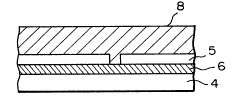
First, as shown in Fig. 4(A) and Fig. 5(A),
` on the base substrate 4 is formed a thin film 6 (or
called "Seed") ~forming nucleation surface (SNDL)
6A~ with greater nucleation density enabling selective
nucleation, on which a material different from the `~
- material for~ing the thin film 6 with greater nucleation
density is thinly dep~sited, followed by patterning
25 according to lithography, etc., to form a thin film -~ ~
~-~ 5 comprising a different material and forming non- ~ ~ -
nucleation surface (SNDs) 5A so as to provide
^ -
- 20 - 1 3 3 0 1 91
1 sufficiently finely nucleation surfaces (SNDL) 6A.
However, the size, the crystal structure and composition
of the base substrate 4 may be chosen as desired,
and it may be also a substrate having a functional
device prepared according to conventional semiconductor
technique formed thereon. Also, the nucleation
surface (SNDL) 6A comprising a different material
may be also formed as a modified region containing
excessive Si or N, which may be formed by forming
a thin film 6 beneath the SiO2 thin film 5 of a
polycrystalline silicon or SiO2, and injecting ions
of Si or N into the exposed portions 6A.
Next, by selection of appropriate deposition
conditions, a single nucleus of crystal formation -
1~ material is formed only on the nucleation surface
~SNDL) 6A. That is, the nucleation surface (SNDL)
6A is required to be formed sufficiently minutely
so that only a single nucleus may be formed thereon.
The size of the nucleation surface (SNDL) 6A, which
;20 may differ depending on the kind of the material,
may be several microns or less. Further, the nucleus
grows while maintaining a single crystal structure ~ -
to become a single crystal grain 7 in shape of an
island as shown in Fig. 4(B). For forming an island-
shaped single crystal grain 7, it is desirable to
determine the conditions so that nonnucleation may
occur at all on the thin film 5A, as already mentioned.
.~
13301~1 :
- 21 -
1 The island-shaped single crystal grain 7 further
grows while maintaining the single crystal structure
with the nucleation surface (SNDL) 6A as the center
(lateral overgrowth), whereby it can cover over the
whole surface of the thin film 5 as shown in Fig.
4(C) (single crystal 7A).
Subsequently, if necessary, the single crystal
7A is flattened by etching or polishing, and a single
crystal layer 8 capable of forming a desired device
can be formed on the thin film 5 as shown in Fig.
4(D) and Fig. 5(B). -
Thus, due to formation of the thin film 6
;; forming the nucleation surface (SNDL) 6A on the substrate
4, any desired material can be used for the substrate ;~
15 4 which is the supporting member. Further, in such ~
a case, even when the substrate 4 may be one having ~ ;
a functional device, etc., formed thereon according ~ ~
~; to conventional semiconductor technique, the single ~ ;`
crystal layer 8 can be easily formed thereon.
In the above embodiment, the nucleation surface
(SNDL) 6A is formed of thin film 6, but a substrate
comprising a material with large nucleation density
~ ND) enabling selective nucleation may be used as
ri~ such and nonnucleation surfaces (SNDs) may be provided -~;
25 at any desired positions to form single crystal layers ; `~
similarly thereon as shown in Fig. 6.
Figs. 6(A)-6(D) are illustrations of the steps ~ -
- :~, .
;~
` . . ~
--22 ~33~1~t
' ' '' '
1 for forming crystal showing a second embodiment of
the present invention. As shown in these figures,
on a substarte 9 comprising a material with large
nucleation density (ND) enabling selective nucleation,
the nonnucleation surface (SNDs) comprising a material
with small nucleation density (ND) can be formed so
as to give exposed portions ~jf the substrate 9 as
nucleation surface (SNDL) 9A sufficiently minutely
to form a single crystal layer 8 similarly as in the
first embodiment.
Figs. 7(A)-7(D) are illustrations of the
formation steps showing a third embodiment of the
method for forming crystal according to the present
invention, and Figs. 8(A) and 8(B) are perspective
.. . .
`~ 15 views corresponding to Figs. 7(A) and 7(D). ~ -
; As shown in Fig. 7(A) and Fig. 8(A), on an
appropriate base substrate 10 such as glass substrate,
etc., an amorphous insulating thin film 12 with relatively
~` greater nucleation density (ND) such as Si3H4, etc., ;
is provided, and on said thin film 12 is formed
' selectively a thin film 11 at a desired position with
a different material having smaller nucleation density
relative to the material forming the thin film 12
which enables the above selective nucleation with
an interval of a distance ~, thereby arranging nucleation
5~ surfaces (SNDL) 12A-1, 12A-2 with sufficiently small -
`~ areas so as to form only single nucleus thereon.
:` :
- 23 - 1330191
I This distance Q may be set at a size which is equal
to or greater than the size of the single crystal -~
region required for formation of a semiconductor device
or a group of devices.
J Next, by selecting appropriate crystal forming
conditions, on the nucleation surface (SNDL) 12-1,
12-2 only a nucleus of a crystal forming material is
formed. That is, as described above, the nucleation
surfaces 12-1, 12-2 are required to be formed to a -~
sufficiently iine size (area) to the extent that only
a single nucleus may be formed. The size of the ~ - -
: .. : .. : .
nucleation surfaces (SNDL) 12-1, 12-2, which may be
different depending on the kinds of the material,
may be several microns or less. Further, the nucleus
formed as above grows while maintaining the single
crystal structure, and become island-shaped single
crystal grains 13-1, 13-2 as shown in Fig. 7(B).
For forming island-shaped single crystal grains 13- ~ -
1, 13-2, it is desirable to determine the conditions
`~t~ 20 so that substantially no nucleation may occur at all ~
on other surfaces than the nucleation surfaces (SNDL) ~ ~ ;
12A-1, 12A-2, tnonnucleation surface (SNDs) llA~.
The crystal direction in the normal line
direction of the thin film 12 of the island-shaped
single crystal grains 13-1, 13-2 is determined so
as to make the interface energy of the material of ~- ~
. ,': '..': ~:
, ,, , . .~: :.,:
- 24 ~ 1 3 3 0 ~ 9 ~
1 the film 12 and the material forming nucleus minimum.
For, surface or interface energy has anisotropy depending
on the crystal face. However, as already mentioned, the
crystal direction within the surface plane in amorphous
surface is not determined.
The island-shaped single crystal grains 13-1, 13-2
further grow to become single crystals 13A-1, 13A-2 until
the adjacent single crystals 13A-1, 13A-2 contact each
other as shown in Fig. 7~C), but since the crystal
10 directions within the substrate plane vary from one single
; crystal to another, a crystal grain boundary 14 is formed
;~ at the intermediate position between the nucleation
~ surfaces (SNDL) 12-1 and 12-2.
`~ Subsequently, the single crystals 13A-1,
13A-2 grow three-dimensionally, but crystal faces
with slow growth speed appear as the facet. For this
reason, the surfaces of single crystals 13A-1, 13A-
2 are flattened by etching or polishing, and further
the portion of the grain boundary 14 is removed to
form thin films of single crystals 15-1, 15-2, ...
',, containing no grain boundary in shape of lattices
~3 ~
as shown in Fig. 7(D) and Fig. 8(B). The size of
the single crystal films lS-l, 15-2, ... is determined
by the interval Q betw~en the nucleation surfaces
7~
,,'?"`~ 25 `(SNDL) 12A-1, 12A-2 as described above. That is, -
by determining appropriately the formation pattern
of the nucleation surface (SNDL) 12A-1, 12A-2, the
position of the grain boundary can be controlled to
~ ..
- 25 - 133~
I form single crystals with desired sizes at a desired
arrangement.
Figs. 9(A)-9(C) are illustrations of the
formation steps showing a fourth embodiment of the
method for forming crystal according to the present
invention, and Figs. 10(A)-lO(B) are perspective views
of the substrates in Figs. 9(A) and 9(C).
First, as shown in Fig. 9(A) and Fig. lO(A),
similarly as shown in the step (A) in Fig. 1, thin
10 films 12 and 11 are provided on the base substrate - ;~
10 to form nucleation surfaces (SNDL) 12A-1, 12A-2
and nonnucleation surface (SNDs) llA. Subsequently,
so that concavities 14-1, 14-2 with desired sizes
and shapes may be provided at the corresponding positions
1~ to the nucleation surfaces (SNDL) 12A-1, 12A-2, a
thin film 11-1 is formed with the same material as
the thin film llA or a material having nucleation
density equal to or smaller than said material. Thus,
`~ a substrate for formation of crystal having nucleation
~:
surfaces (SNDL) 12A-1, 12A-2 with sufficiently fine
sizes for forming only single nucleus within concavities - ;
14-1, 14-2 is formed. -
Subsequently, as shown in Fig. 9(B), island-
shaped single crystal grains 13 are grown similarly
25 as in the first embodiment. -
And, as shown in Fig. 9(C) and Fig.lO(B),
single crystal grains 13-1, 13-2 are grown until
. . ! :.. ;,; . .. . ! , ~ ..
1330191
- 26 -
I embedding the concavity 14-1, 14-2 to form a single
crystal layer 15-1, 15-2.
In this embodiment, since single crystal grains
13-1, 13-2 grow within the concavity 14-1, 14-2, the
steps of flattening and removing the grain portion
may be unnecessary.
Fig. 11 is a schematic sectional view showing
an example of the semiconductor electronic device with
a multi-layer structure produced by use of the first
embodiment of the present invention.
In Fig. 11 on the semiconductor substrate -
1101 such as Si or GaAs, transistors 1102 or other
semiconductor devices or optical devices are formed,
. ;~ ,.
and Si3N4 layer 1104 having, a surface for formation ;
~-~ 15 of, for example, nucleation surface (SNDL) 1105 is
,. . .
'a`" formed thereon according to the CVD method or the
~` sputtering method. And, as already mentioned, nucleation
surfaces (SNDL) 1105 are exposed as sufficiently minute
'~,s~ . -
areas so that only a single nucleus may be formed
and a thin film 1106 of, for example, Si3N4 having
nonnucleation surface (SNDs) 1107 is formed and from
t~ said nucleation surface (SNDL) 1105 single crystal
layer 1108 is formed. In the Figure, 1103 denotes
SiO2 layer.
l~; 25 Subsequently, on the single crystal layer
.,~
1108 are formed transistors 1109 or other semiconductor
devices or optical devices, and the devices formed
.~
~`, ' ` ' ,
' "`, ' ' '. " ,, . ''' `' ' .' . '~, ' ' . . .' ." :' '', ' " :
. .
1 3 3 0 1 9 1
- 2 7 - ~ `
I respectively on the substrate 1101 and the Si single
crystal layer 1107 are electrically connected through
the Si3N4 layer 1104. Thus, for example, by forming
the transistor 1102 of the first layer (substrate
1101) and the transistor 1109 of the second layer
(single crystal layer 1108) respectively as the MOS
transistors, and connecting these to form CMOS, a
CMOS entirely free from mutuai interaction can be
produced. Also, according to the technique as described
i0 above, an electroluminescent device can be also formed
integrated with its driving circuit to accomplish
a high degree of integration. -
Further, by repeating this embodiment, single
crystal layers 1108 can be formed in many layers with -
, ~ . . . -
~ 15 Si3N4 layer 1104 sandwiched therebetween, whereby
; ", . .;-
a semiconductor electronic device with a multiple ~;
structure can be formed easily. ~ ;
~- ; Figs. 12(A)-12(D) are illustrations of the ~;-
steps for forming crystal showing an fifth embodiment -~
~ 20 of the present invention. Figs. 12(A)-12(C) are the -
,'~ same as Figs. 7(A)-7(C). That is, a plurality ,~
(two in the Figure) of nucleation surfaces 12A~
12A-2 are formed with an interval of Q, and single crystal ~ ~
grains 13-1, 13-2 sub~lected to over growth on the ~ -
`~ 25 nucleation surfaces 12A-1, 12A-2 are formed. By ,- --
permitting the single crystal grains 13-1, 13-2 to
further grow to form single crystals 13A-1, 13A-2 ~,
:~
} ~, ~ . .. : .
-,.:. :.'. :,..
. ' ' ' ~ ' ' ' ' ! ' ~ ' ; : ' ` ` ~
- 28 - 1330191
1 a grain boundary 14 is formed approximately at the
sentPr between the nonnucleation surfaces (SND5) llA,
and by flattening the surface of single crystal 13A-
1, 13A-2 a polycrystalline layer 16 with regular grain
sizes which are approximately equal to Q as shown
in Fig. 12(D) can be obtained.
Since the grain size of the polycrystalline
layer 16 is determined by the interval Q between the
nucleation surfaces (SNDL) 12A-1, 12A-2 , it becomes
possible to control the grain size of the polycrystal.
In the prior art, the grain size of a polycrystal
was changed by a plural number of factors such as
the formation method, formation temperature, etc.,
-~` and also when preparing a polycrystal with large grain
; 15 size, it had a grain size distribution with a considerable
width. However, according to the present invention,
,~ the grain size and grain size distribution can be
determined with good controllability by the interval
l between the nucleation surfaces (SNDL) 12A-1, 12A-
2-
~' Of course, as shown in Fig. 6, polycrystal
-iayer 21 may be formed as above by forming a thin
film having nonnucleation surface ~SNDs) SA with small
nucleation density (ND~ on a desired substrate 9 and
~,, .
` 25 plural nucleation surafces (SNDL) 9A with greater
nucleation density (ND) at desired positions and
~; intervals. In this case, as already mentioned, the
.
, ,: `
~33019i
- 29 -
I substrate material and structure are not limited provided
that the nucleation density difference (~ND) is taken
into consideration but the polycrystal layer can be
formed by controlling the grain size and the grain
size distribution.
Next, the specific ~ethod for forming a single
crystal layer or a polycrystal layer in the above
respective embodiments is described in more detail
by referring primarily to the third embodiment shown
in Fig. 7.
:: : .-:
By thermal oxidation of a Si single crystal
wafer to form a SiO2 layer on the surface and subsequent
thin film formation of Si3N4 or polycrystalline Si
layer to a desired thickness by the reduced pressure
,.. ..
chemical vapor deposition method, a surface with a
large nucleation density (ND) is obtained. Of course,
a quartz substrate which is a material with small ~-
nucleation density (ND) can be also used as a base -- ::
- substrate 10, or alternatively a surface with a large -
;` 20 nucleation density (ND) may be provided by forming
`' a thin film 12 of Si3N4 or polycrystalline Si layer
on the surface of any desired base substrate such
as metal, semiconductor, magnetic material, piezoelectric
material, insulator, etc., by use of the sputterin~ -
method, the CVD method, the vacuum vapor deposition
method, etc. Also, as the material for formation
of the thin film 12 partially providing nucleation
. ' ,.:
' ~ ~ ' . ,.
.~ ~
~ 30 ~ ~33~19~
I surfaces (SNDL), SiO2 is desirable, but SiNx
(0 < x < 4/3) with the value of x being varied may
be also employed.
On the above thin film 12 thus formed on
the substrate 10 is deposited a thin film 11 of SiO2
or SiOy (0 < Y < 2) according to the reduced pressure
chemical vapor deposition method, and subsequently
the above thin film 11 is subjected to patterning
according to conventional lithographic technique
or lithographic technique by use of X-ray, electron
beam or ion beam to selectively exposed the surface of
the thin film 12, whereby nucleation surfaces (SNDL)
12A-1, 12A-2 having fine area of preferably 10 ,um or
less, more preferably several microns or less, optimally
about 1 ~um or less, are obtained.
Subsequently, by use of SiH2C12, SiC14, SiHC13
SiF4 or SiH4 or a gas mixture of these, optionally
;~ mixed with HCl, H2 or a gas mixture of these, Si
~`~ single crystal is selectively grown on the above
nucleation surface (SNDL) 12A-1, 12A-2-
The substrate temperature, pressure, etc.,
may be conveniently determined, but the substrate
temperature may be preferably 700 to 1100 C, and
the pressure may be pr~sferebly about 100 Torr.
2~ Within a time of about some 10 minutes, by
selection of optimum growth conditions, grains 13-
. ~
~,
~: '
- 31 ~ 1330191
I 1, 13-2 of single crystals of Si grow on the nucleation
surfaces ( SNDS ) 12A-1, 12A-2 as the center, and grow
to sizes of some 10 )um or more.
.
. "'., .:
. " :: ;.
.: - . . .. '
/ :~ :
'`'" / ' - ~''
25 / : ;~
~.
r ~
- 32 - 1330191
1 Subsequently, by the reactive ion etching (RIE)
method utilizing the etching speed difference between Si
and SiO2, the surfaces of the single crystals 13A-1,
13A-2 are flattened by selective etching of only Si,
5 whereby a polycrystalline silicon layer controlled in ~ -
grain size can be formed. Further, by removing the
grain boundary portion, island-shaped single crystalline
silicon layers 15-1, 15-2 are formed (Fig. 7(D)). If
unevenness on the surface of the single crystal grains
l0 13A-1, 13A-2 are large, mechanical polishing may be
conducted before etching. When electrical field effect
transistors are formed according to conventional semi-
conductor device preparation technique on the single
crystal silicon layers 15-1, 15-2 thus formed with a
size of some 10 ~um or more containing no grain boundary, `
characteristics not inferior to that formed on single
1..
silicon wafer are exhibited.
Also, mutual interference between the adjacent
~ single crystal silicon layers can be prevented, if they
``';~ ` 20 are electrically separated by an electrical insulator
such as SiO2, even if a complementary type electrical
'i~ 'field effect transistor (C-COM) may be constituted.
~`;; Also, since the thickness of the active layer of
the device formed is thinner than the case when employing
~; 25 Si wafer, there is no erroneous actuation by the `
charges generated when radiation is irradiated. Further,
~`1 due to lowering in unwanted capacity, speed-up of the
: ~ ~
~ ~:
33 1330191 - -
~, , ,
:: 1,,. '
I device can be effected. Also, since any desired
substrate can be used, a single crystal layer can be ~ ~-
:: .
formed on a substrate of large area at lower cost than - - `
.. .. .
when employing Si wafer. Further, since a single crystal
layer can be formed also on other semiconductors,
piezoelectric materials, dielectric materials, etc., -
a multi-functional three-dimensional integrated circuit
can be realized. Thus, the present invention exhibits ;~ -
a number of excellent effects.
(Composition of silicon nitride)
For obtaining sufficient nucleation density
difference (~ND) between the material (Ms) for formation
of nonnucleation surface (SNDs) and the material (ML)
for formation of nucleation surface (SNDL) as described
15 above, for polycrystalline silicon or SiO2 as the -
material for formation of nonnucleation surface (SNDs) -
-~ to be used in combination, the material for formation of -~ i
~ nucleation surface (SNDL) is not limited to Si3N4, but
~iv ~ , ' '
';; silicon nitrides with various chemical composition ratios
may be employed.
The chemical composition ratio of silicon
nitride may be varied e.g. as follows.
In the plasma CVD method for forming silicon
~ nitride film at low temperature by decomposition of
`` 25 SiH4 gas and NH3 gas in RF plasma, by varying the flow
rate ratio of SiH4 gas and NH3 gas, the composition
` ratio of Si and N in the deposited silicon nitride film
,.
;
. ~ . .. . - . . . .. . . ,, , , , . . . ,. ~
:: !
- 34 - 1 3 3 ~ 1 9
can be varied to a great extent.
Fig. 13 is a graph showing an example of the
relationship between the flow rate ratio of SiH4 and
NH3 and the composition ratio of Si and N in the
silicon nitride film formed.
The deposition conditions at this time were RF
output of 175 W, substrate te.mperature of 380 C and
the flow rate of NH3 gas was varied with the SiH4 gas
flow rate being fixed at 300 cc/min. As shown in the same
graph, by varying the gas flow rate ratio of NH3/SiH
from 4 to 10, the Si/N ratio in the silicon nitride
film was found to be varied from 1.1 to 0.58 according
to Auger's electron spectrophotometry.
On the other hand, the composition of the silicon
nitride film formed according to the reduced pressure
CVD method by introducing SiH2Cl2 gas and NH3 gas under
~`~; the conditions of a reduced pressure of 0.3 Torr and a ;~
temperature of about 800 ~C was found to be Si3N4
(Si/N - 0.75) which is approximately the stoichiometric -~`
` 20 ratio-
Also, the silicon nitride film formed by heat
treatment at about 1200 C in ammonia or N2 (hot -~
nitrification method) can be obtained with a composition
,n ' i further approximate to the stoichiometric ratio, since -~
.~
the formation method is performed under thermal
equilibrium.
~ By use of silicon nitrides formed by the various ~ ~ ;
:~
- 35 ~ 1 3 3 0 1 9 1
I methods as described above as the material for forming
nucleation surface (SNDL) with higher nucleation density
than SiO2, the above nucleus of Si can be grown on the
nucleation surface (SNDL) comprising silicon nitride to
form Si single crystal based on the nucleation density
(~ND) corresponding to the chemical composition ratio
of silicon nitride. .
Fig. 14 is a graph showing the relationship
between Si/N composition ratio and nucleation density
(~ND). As shown in the same graph, by varying the
chemical composition ratio of the silicon nitride film,
the nucleation density of the Si single crystal nucleus
formed thereon changes to a great extent. The nucleation
conditions in the graph shown in Fig. 14 correspond to
; l5 the case when Si single crystal nucleus was formed by
~ reacting SiC14 gas reduced to 175 Torr with H2 at
-~ 1000 C. Of course, another graph will be obtained if
nucleation conditions such as gas species, pressure,
~ temperature, etc., are changed.
```~ 20 The phenomenon that the nucleation density thus
changes according to the chemical composition ratio of
silicon nitride affects the size (area) of the nucleation
` surface (SNDL) when employing silicon nitride as the
¦ material for forming 1:he nucleation surface (SNDL) which
1 25 is formed sufficiently finely to the extent that a
¦ single nucleus may be grown. That is, when employing
i silicon nitride having a composition with great
,
1330191
- 36 -
nucleation density (ND) only a single crystal can be
formed on the nucleation surface (SNDL) by forming the
nucleation surface (SNDL) extremely finely as compared -
with the silicon nitride with relatively smaller
nucleation density (ND). Such a point is applicable
as a similar tendency for other materials for forming
nucleation surface (SNDL). Accordingly, in the present
invention, for accomplishing its objects effectively,
it is desirable to select a nucleation density (ND) and
. . .
a size of nucleation surface (SNDL) formed of silicon
nitride, etc., capable of forming only a single crystal ~ -
suitably as desired. For example, under the nucleation
' condition for obtaining a nucleation density (ND) of ~-
about 105 cm 2, it is possible to form selectively only
15 a single nucleus, if the size of the nucleation surface ~-
(SNDL) comprising silicon nitride is about 4 /um or less.
The Si/N ratio in that case is about 0.5.
~- (formation of nucleation surface (SNDL) by ion
injection)
~` ~ 20 As another method for realizing nucleation
~i density difference (~ND) when forming Si single crystal ;~
nucleus, ion injection of N, P, B, F, Ar, He, C, As,
` Ga, Ge, etc., may be effected locally onto the single
crystal Si surface of the above substrate provided at
` 25 desired positions and intervals with SiO2 thin layer
~` which is a material for forming nonnucleation surface
(SNDs) with smaller nucleation density thus resulting
, ~ .
j ~ ~ . " :- :
~ ~" S ~
1330191
- 37 -
I in partial exposure of the single crystal surface to
form a modified region, and utilize this modified region
as the nucleation surface (SNDL) with greater nucleation
density (ND).
For example, the SiO2 layer surface given on the
single crystal Si substrate is covered with a photo-
resist layer and the desired portions are exposed,
developed and dissolved to have the surface of the
single crystal Si substrate exposed.
Subsequently, while the remaining photoresist
layer is left as it is, by use of NH3 gas as the source
gas, N ions are implanted onto the single crystal Si
layer surface portion exposed at 15 keV at a density of ;
1 x 10¹⁶ - 1 x 1013 cm 2. The projected flying distance
in this case is 120 A, and the N concentration on the
exposed surface of single crystal Si layer reaches
. ~ .
-- about 1022 cm 3. The modified region made excessively
~ enriched in N by injection of N ions is amorphous.
,~ .
For formation of a modified region, ion
injection can be effected with the use of a resist as
the mask, but it is also possible to inject a narrowed
N ion beam selectively at an exposed single crystal Si
portion of the layer surface without use of a resist mark
~ by use of converged ion beam technique.
;~ 25 After having thus effected N ion injection, by
peeling of the resist on the remaining portion, N-
excessive modified region is formed in the single
.,
1330191
- 38 -
I crystal Si layer surface at a desired position with a
desired size. On the modified region of the substrate
for crystal growth having such modified region formed, - -~--
Si single crystal is permitted to grow in vapor phase.
(Method for formation of Si single crystal nucleus
other than CVD)
For growth of single crystal by selective
nucleation of Si, not only the CVD method, but also the ~ --
method by evaporation of Si into vacuum t~ 10 6 Torr)
with an electron gun and deposition on a heated
~ . .:
~ substrate may be used. Particularly, in the MBE
: , .- .- ~ .;
~` (Molecular Beam Epitaxy) method which performs vapor ;
deposition in ultra-high vacuum (< 10 9 Torr), it has
been known that Si begins to react with SiO2 at a
` ~ 15 substrate temperature of 900 ~C or higher, whereby no
nucleation of Si occurs on SiO2 at all (T. Yonehara,
S. YoshioXa and S. Miyazawa, Journal of Applied Physics `
53, 10, p. 6839, 1983).
8y utilizing this phenomenon, single crystal
nuclei of Si can be formed with perfect selectivity on
the fine silicon nitride regions permitted to exist in
' spots on the SiO2 thin film by giving concavities and
- exposing it, and single crystal Si can be grown from
the nuclei. The single crystal growth conditions as ~ ~
preferable example at this time may be, for example, a - --
~ . :
vacuum degree of 10 8 Torr or lower, Si beam intensity ;
~ of 9.7 x 10¹⁴ atoms/cm2-sec, and a substrate temperature
`~ of 900 C - 1000 C.
- 39 ~ 1 3 3 ~ 1 9
I In this case, through the reaction SiO2 + Si ~
2SiO~, a reaction product of SiO with a remarkably high
vapor pressure is formed, and etching of SiO2 itself
with Si through this evaporation occurs.
In contrast, no such etching phenomenon as
mentioned above occurs on silicon nitride thin film, but
nucleation of Si single crystal and growth of single
crystal occur.
Accordingly, as the material for forming
nucleation surface (SNDL) with high nucleation density
(ND), tantalum oxide (Ta2O5), silicon nitride oxide
(SiON), etc., can be also used other than silicon
nitride to obtain the same effect. That is, by forming
the above nucleation surface (SNDL) with these materials
in f ine areas, single crystals of Si can be permitted
to grow similarly.
(Crystal growth of material other than Si)
~1) As the crystalline material other than Si, the case
of diamond is shown as an Example, as already mentioned,
,,~, j .
it has been desired to apply a diamond thin film as the
semiconductor for electronic device, it has been
, ;
impossible in the prior art to grow a diamond single
~ crystal on a material other than the diamond substrate.
;~ However, according to the crystal growth method
according to the present invention, a diamond single
crystal can be easily grown on a material other than
diamond substrate. Here, explanation is made about an
,
.~ , - i i :,,: .-
~ 40 - 1 3 3 0 19 1 !
.
I example of forming a single crystal of diamond by -
utilizing the fact that no single crystal nucleus of
diamond grows on the surface of a metal such as Fe or
Co.
First, on a desired base substrate, a thin film
of a metal such as Cu, W, Ta, Mo, Au, Ti, Al, Ni, etc., ;
is deposited according to the vacuum vapor deposition
method, or a semiconductor material thin film such as of
Si, Ge, GaAs, InP, SiC, etc., according to the CVD method
or the vacuum vapor deposition method. These thin films ;
(FL) form nucleation surfaces (SNDL) having a large ; - -
nucleation density (ND) mentioned in this specification.
Subsequently, on the film (FL)I a metal thln film of
-~ Fe or Co is formed by the vacuum vapor deposition method.
This metal thin film has a polycrystalline structure.
These metal films (Fs) have a sufficient smaller
nucleation density as compared with the above thin film
(FL). Subsequently, the above thin film (Fs) is
subjected to patterning so as to expose the above film
FL) to a size of several micrometer to form a nucleation
surface (SNDL) with a sufficiently minute area.
,; Thus, single crystal diamond is crystallized on
the nucleation surface under the following conditions.
As the method for crystallization of diamond,
there may be employed the CVD method according to the ~-
.~ microwave plasma CVD method, the hot filament method,
etc. As the starting gases, for example, there may be
I
! i ~ - ~
~33~91
- 41 -
1 employed gas ~ixtures of methane (CH4) and hydrogen
(1 - 10 %), or hydrocarbons having alcoholic OH groups,
specifically methyl alcohol CH30H, ethyl alcohol
C2H5OH, tert-butyl alcohol (CH3)30H, isopropyl alcohol
(CH3)2)CHOH, diethyl ether C2H5OC2H5, etc-, by bubbling
these liquids with hydrogen gas.
In the case of the plasma CVD method, it can
be practiced, for example, under the conditions of a
microwave output of 200 to 350 W, a substrate temperature
of 500 to 1000 C and a reduced pressure of 1 to 400
Torr.
In the case of the CVD method by use of the hot
filament method, it can be practiced, for example, under -
~ .
-~ the conditions of a filament temperature of about 1500
15 to 2000 C and a filament-substrate distance of 0.5 to
;~i 10 mm.
As the result, no nucleation of diamond occurs
at all on the metal thin film (Fs) of Fe or Co, but only
. ~
r,~ ~ a single diamond single crystal nucleus is formed on the
nucleation surface (SNDL) with higher nucleation density
(ND) minutely formed by exposing the thin film (FL) out
'~ of the thim film (Fs), and thereafter diamond grains
of single crystals grow to the sizes of some 10 ym to
some 100 ym with the single diamond nuclei as their
centers. In these diamond grains, there may sometimes
exist internally the twin crystal grain boundaries
without unpaired electrons depending on the crystal
` - .
, , ~ ~ ~ . ' . , . : , ! I '~ . ' . ' ` ` ~ ' i
! ':
1330191
I forming conditions, but there exists no grain boundary
containing much unpaired electrons as found in the so
called polycrystalline structure. This is because growth
of a diamond single crystal from a single nucleus formed
on the nucleation surface (SNDL) is not inhibited due
to absence of formation of diamond nucleus on the non-
nucleation surface (SNDS) formed of a material such as ;~
Fe or Co with lower nucleation density.
Fig. 15 is a graph showing the time dependencylO of nucleation density of the diamond on the surface of
Fe, Co, Si, Mo.
As shown in this graph, it is possible to take
sufficiently a difference in nucleation density of
diamond on the surface of a metal of Fe, Co and on the
`~ 15 surface of Si, Mo. This point is the same as in the
case of nucleation density of Si on the surface of ~ ~:
Si3N4 and on the surface of SiO2 shown in Fig. 3. `-~ - .
Thus, by forming a layer for formation
nucleation surface (SNDL) with higher nucleation density
(ND) on the base substrate of any desired material
~` other than diamond substrate, and thereon forming a ~ ~~
thin film giving nonnucleation surface (SNDS) with ` '`~
lower nucleation density (ND) so as to expose the -
`~; surface of the above thin film (FL) selectively at a
;```~; 25 sufficiently minute area, diamond single crystal can
be formed with ease using the thus obtained substrate
for crystal formation. Of course, as already mentioned,
` ~ ~'' ''' ' '
1 ~ ,-,~ .: . .. ,: . ~
_ 43 _ 1 3 3 01 91
1 it is possible to form a diamond thin film of a poly-
crystalline structure with controlled grain size by
arranging nucleation surfaces ~SNDL) having fine areas
at desired intervals.
Also, according to the present invention, as the
base substrate, it may in principle be a substrate of
the material capable of forming a thin film (FL) giving
the above nucleation surface (SNDL), and therefore the
selection scope can be broadened to a great extent to
accomplish lo~ cost and enlargement of area with ease.
(2) Growth of tungsten signle crystal
Tungsten has been known to effect no nucleation
on the surface of SiO2 layer, but to be deposited as a
polycrystalline film on Si, WSi2, PtSi, Al, etc.
~; 15 First, on a suitable substrate, a thin film
(FL) of Si, WSi2, PtSi or Al is deposited by vacuum ~ -
vapor deposition. These films provide surfaces forming
nucleation surface (SNDL). Next, on the thin film (FL)
comprising the above material, a thin film (Fs) compris-
~; 20 ing a material with small nucleation density (ND) such - -
Zl as SiO2, etc., is formed according to the heat oxidation
treatment, hot CVD, PCVD, sputtering, etc. Then, the
substrate subjected to patterning so as to expose the
above thin film (Fs) to a size of several ~um or less by
photolithography to form a desired number of nucleation
surface (SNDL).
Subsequently, the substrate for crystal formation
- 44 - 1 3 3 0 1 9 1
I prepared as above is placed in, for example, a reaction
furnace heated to 250 - 500 C, and a gas mixture of WF6
gas and hydrogen gas is permitted to flow under a
reduced pressure of about 0.1 to 10 Torr, at the respective
flow rate of 75 cc/min and 10 cc/min.
By doing so, tungsten is formed as represented
by the reaction scheme WF6 + 3H2 ~ W + 6HF. In this
. :
case, the reactivity of tungsten with SiO2 is
extremely low to give no firm bonding, and therefore no
10 nucleation occurs on the surface of the thin film (Fs) ;
of e.g. SiO2 and hence no deposition is effected. -
In contract, on the above nucleation surface ~ -
(SNDL) formed of a thin film (FL) of Si, WSi2, PtSi, -
Al, etc., single crystal nuclei of tungsten are formed ,,-
single crystal nuclei of tungsten singly, because
nucleation surfaces (SNDL) are formed minutely. And,
` the single crystal of tungsten continues to grow and ~
also grows as such single crystal also in the lateral ; - -- -;
direction on the thin film (Fs). This is because
20 nonnucleus growth of tungsten occurs on the thin film -
` (Fs), whereby no polycrystal is formed by interference
of single crystal growth.
The combination of the nonnucleation surface ~-
~SNDs) forming material, nucleation surface (SNDL) -~
forming material and crystal forming material as
described above is not limited to those shown in the
above embodiments, but it may be clearly a combination
~ 45 - 1330191
of materials having sufficient nucleation density
, difference (~ND). Accordingly, also in the case of a
¦ compound semiconductor capable of selective nucleation
¦ such GaAs, InP, etc., a single crystal, a group of
j 5 single crystals or a polycrystal controlled in grain
! size and grain size distribution can be formed according
to the present invention.
~ Example 1
¦ A 5 inch Si single crystal wafer was set in a
¦ 10 reduced pressure chemical vapor deposition device and
Si3N4 layer was formed to a thickness of 300 A (formation
: of nonnucleation surface (SNDs)) according to the hot
~ CVD method under the deposition conditions as follows. -:.
-~ Pressure ............... 0.3 Torr
Gases used ............. SiH2C12 + NH3 gas mixture
Flow rate ratio ........ NH3/SiH2C12 = 7
Temperature ............ 820 C
Next, the above Si single crystal wafer having
` Si3N4 layer formed thereon was set in a reduced
i,.~ - :
pressure chemical vapor deposition device, and a SiO2
` layer was formed to a thickness of 500 A on the Si3N4
layer according to the hot CVD method under the
following deposition conditions. .
Pressure ............... 1.0 Torr -
: 25 Gases used ............. SiH4 + N2O
Flow rate ratio ........ SiH4/N2O = 5
: Substrate temperature .. ...700 C
.. ~ .
- 46 _ 1330~9~ i
I Next, the above SiO2 layer was subjected to
patterning according to X-ray lithographic technique
to form Si3N~ minute regions for nucleation surfaces
(SNDL) of Si~N4 exposed thereat in a matrix arrangement
of 50 x 100 with sizes of 1 ym and 150 ~m pitch.
On the Si single crystal wafer having thus ~,
provided nonnucleation surface comprising SiO2 (SNDs) '
and nucleation surfaces (SNDL) of 50 x 100 of Si3N4 '
exposed thereat, Si single crystals were grown ', ~'
10 according to the hot CVD method under the Si single, ,~
crystal growth conditions shown below. , , ,-,'- -
Pressure ................. 150 Torr ,,
Gases used ............... SiH2Cl2
Flow rate ................ 1.2 liter/min ,, -,, -~
15 Temperature .............. 1030 C ~ -''-'-
Crystal growth time ...... 40 min -'
The Si single crystal wafer applied with the
crystal preparation treatment was taken out from the
~, device, and the crystal was evaluated by observation ~' ;
' 20 with an electron microscope and X-ray diffraction. ~' -
As the result, it was found that 50 x 100 Si single ' ',
crystals with grain size of 80 ~m and substantially no ', , ',
grain size distribution were formed with the above
region of exposed Si3N4 as the center.
All of these Si sin~le crystals were shown
to have single crystal properties of extremely good
quality. ' '
~ 47 ~ 1 3 3 0 1 9
I Example 2
Under the same conditions as in Example 1 except
for taking sufficiently the time for growth of Si single
crystals, an Si polycrystalline layer comprising the state
in which adjacent Si single crystals mutually contact
each other as shown in Fig. 12(D) was formed. On the
surface of the polycrystalli~e layer, smoothening treatment
was applied according to the selective etching method
as conventionally practiced in the field of semiconductors.
By use of the Si polycrystalline layer having
thus smoothened surface, P-MOS transistor was prepared
according to the method conventionally used in the field -
:~ of semiconductors and actuation characteristics were
measured. As the result, it was found to be by far superior
to the case of P-MOS transistor formed by use of the Si
polycrystalline layer obtained according to the prior
art method.
Example 3
When Si single crystal group as shown in Fig.
~ ; 20 7(D) was prepared under the growth conditions of substrate
!, ,~ for formation of crystal and the crystal growth conditions
' shown below and oiherwise similar to Example 1, and
~ ~ evaluated in the same manner as in Example 1, the same
^~`; results as in Example 1 were obtained.
,r`: 25 [Substrate growth conditions~
Substrate .......... Si polycrystallien substrate
;, having Si3N4 layer to a ~
` .' ' ~. ,. '.' ~ ' ,
. ~ -
- 48 - 1 3 3 0 1 9 1
I thickness of 300 A provided ~ -;
according to the hot CVD method
Pressure .......... Ø4 Torr : -~
Gases used ....-.-- SiH2C12 + NH3 gas mixture
Flow rate ratio ... .NH3/SiH2Cl2 = 7 ~:
Temperature ....... .850C
Minute region of exposed, silicon nitride [nucleation
~ NDL)~ -
0.5 jum size, 200 /um pitch, 100 x 100 matrix - ~
arrangement ~ -
CCrystal growth conditions~
Pressure .......... 140 Torr
Gases used ........ SiHC13
Flow rate ......... 1.5 liter/min ;
;~ 15 Temperature ....... 1100C
Crystal growth time .... 60 min
Si single crystal which is grown~
Grain size 170 ~m
Substantially no grain size distribution
;- 20 Example 4 P
A single crystal of diamond was prepared as
described below.
¦~ A quartz base substrate was prepared, and an Si
thin film with a thickness of 250 A was provided on its
surface according to the sputtering method. Next, on
~ the Si thin film, a Co thin film was formed to a thickness -~
¦ of 500 A according to the vacuum vapor deposition method
~ by resistor heating.
49 _ 1330191
1 Subsequently the Co thin film was subjected to
patterning treatment according to the photolithographic
method to form a nucleation surface (SNDL) form of thin
film minute region in shape of 100 x 100 matrix with 1
~um size and 100 ~m pitch (formation of diamond single
crystal substrate).
By use of the thus obtained substrate for growth
of single crystals, single crystals of diamond were grown
according to the microwave plasma CVD method under the
following conditions.
Microwave output ......... 300 W
Substrate temperature .... 950C
Pressure ................. 30 Torr
Starting material used ... CH30H (H2 bubbling) -
Flow rate ................ 0.5 liter/min -~
Single crystal of diamond thus obtained had grain
; size of 60 lum substantially without grain size distri~
bution, having extremely good electrical insulation and
excellent thermal conductivity.
~` 20 Example 5
Single crystals of tungsten were grown as described
below.
A Si single crystal wafer was prepared, and an
~ Al thin film with a thickness of 800 A was provided on
3~ 25 its 9urface according to the vacuum vapor deposition method. - ;
ext, on the Al thin film, by use of (SiH4 + 2) gas
mixture diluted with He, a SiO2 thin film was formed to
~3r ~ ` , I
--50 ~ 13 3 0 1~ "
'''~ "''.'~;';"
I a thickness of 500 A according to the plasma CVD method
at a substrate temperature of 300 C.
This SiO2 thin film was then subjected to -
patterning by photolithography into a matrix of 50 x 50
5 with 5 jum size and 100 ~um pitch rpreparation of nucleation ;
surface (SNDL)l-
On the thus obtained substrate for preparation
of tungsten single crystals, single crystals of tungsten
were prepared according to the hot CVD method under the
10 following co~ditions. As a result, the grain size was ~ -~
70 ~um substantially without grain size distribution.
; All of the tungsten crystals formed on the substrate -
- exhibited excellent single crystal properties. ~-
Substrate temperature ...... 300 ~C ~ -~
, .
15 Pressure ................... 1 Torr
Gases used ................. WF6 + H2 gas mixture
.:, ; ~ . .
WF6 flow rate .............. 75 cc/min
H2 flow rate ............... 10 cc/min
Crystal preparation time ... 100 min
As described in detail above, the crystal and
the method for formation thereof according to the present
' invention, by forming sufficiently finely the nucleation ; ~ -
~ : . . ,
surface (SNDL) of a material with sufficiently greater
nucleation density (ND) than the material for formation
~ 25 of nonnucleation surface (SNDs) so that only a single
`~ nucleus may grow, permit single crystals to grow ;
~ selectively at the sites where the fine nucleation surfaces
1330191
- 51 -
I (SND) exist, whereby crystals such as a single crystal
with a necessary size, a plurality of island-shaped
single crystals, a polycrystal controlled in grain size
and grain size distribution, etc., can be formed easily
on a base substrate of any desired material. Besides,
no special new preparation device is required, but it
can be formed by use of a device conventionally used
in semiconductor process.
Also, the crystal according to the present
invention is not limited to the materials of base
substrates as in the prior art, and therefore three~
dimensional integration, enlargement of area and
-~ reduction in cost can be easily accomplished. For
example, since a single crystal or polycrystal of
15 silicon which is the main material of semiconductor ~ -
device can be easily formed on an amorphous insulating
~ material, multi-layer of devices with excellent
2 ~ electrical properties can be accomplished to realize a - ~ ;~
multi-functional integrated circuit not found in the ~
prior art. More specifically, it becomes possible to ~ ; ;
integrate or combine an optical device, a surface
àcoustic device, a piezoelectric device, etc., with thè -~
surrounding circuit IC of the respective devices, etc. `~
~ Also, by use of a cheap glass or ceramic, etc., as the
P~ 25 base material, applicat:ion for a large area electronic
i``~ d~vice such as a large scale flat panel display in which ~1;
; driving circuits are integrated in a sheet of glass,
. ~ ; .: ~ , ., -. .
- - ;
. ~
~330191
- 52 - -
1 etc., is rendered possible. -~
Further, the present invention, by forming the
above nucleation surfaces (SNDL) with desired sizes and
desired distances on the nonnucleation surface (SNDs),
can form single crystals with necessary sizes on a
plural number of sites, and therefore the formation
steps can be simplified to a great extent and also the
formation time can be shortened as compared with the
melting solidification method in which single crystals
are formed by irradiation of laser or electron beam.
Also, by controlling the intervals of the
nucleation surfaces (SNDL) formed on the above non-
nucleation surface (SNDs), a polycrystal controlled in
grain size by the intervals can be formed. In this
.:- .
polycrystal formation method, controllability of grain
size and grain size distribution is good and the
formation time can be also shortened to a great extent
~ as compared with the method of the prior art for forming
!~ a polycrystal with a large grain size according to the ~
~;` 20 above melting solidification method. -
. '
:
4 ~
1~
' '.
, ' ,.
: