Language selection

Search

Patent 1330232 Summary

Third-party information liability

Some of the information on this Web page has been provided by external sources. The Government of Canada is not responsible for the accuracy, reliability or currency of the information supplied by external sources. Users wishing to rely upon this information should consult directly with the source of the information. Content provided by external sources is not subject to official languages, privacy and accessibility requirements.

Claims and Abstract availability

Any discrepancies in the text and image of the Claims and Abstract are due to differing posting times. Text of the Claims and Abstract are posted:

  • At the time the application is open to public inspection;
  • At the time of issue of the patent (grant).
(12) Patent: (11) CA 1330232
(21) Application Number: 607537
(54) English Title: BROADBAND SIGNAL SWITCHING MATRIX NETWORK
(54) French Title: RESEAU MATRICIEL DE COMMUTATION DE SIGNAUX NUMERIQUES
Status: Deemed expired
Bibliographic Data
(52) Canadian Patent Classification (CPC):
  • 344/54
(51) International Patent Classification (IPC):
  • H04Q 3/52 (2006.01)
  • H03K 17/693 (2006.01)
(72) Inventors :
  • TRUMPP, GERHARD (Germany)
  • WOLKENHAUER, JAN (Germany)
(73) Owners :
  • SIEMENS AKTIENGESELLSCHAFT (Germany)
(71) Applicants :
(74) Agent: FETHERSTONHAUGH & CO.
(74) Associate agent:
(45) Issued: 1994-06-14
(22) Filed Date: 1989-08-04
Availability of licence: N/A
(25) Language of filing: English

Patent Cooperation Treaty (PCT): No

(30) Application Priority Data:
Application No. Country/Territory Date
88112908.4 European Patent Office (EPO) 1988-08-08

Abstracts

English Abstract


ABSTRACT OF THE DISCLOSURE
In a broadband signal switching matrix network
having a cross-point matrix in FET technology whose
switching elements, controlled by a holding memory cell,
are each formed with a series circuit of a switching
transistor and of an input transistor. Matrix output
lines thereof are respectively connected to one terminal
of the operating voltage source via a pre-charging
transistor that is controlled by a pre-charging clock,
that side of the series circuit connected opposite from
the matrix output line being permanently connected to the
other terminal of the operating voltage source (directly
or via a transistor controlled by the output signal and
individually associated to the matrix output line) in
order to avoid sample clock lines that lead to the
switching elements.


Claims

Note: Claims are shown in the official language in which they were submitted.


THE EMBODIMENTS OF THE INVENTION IN WHICH AN EXCLUSIVE
PROPERTY OR PRIVILEGE IS CLAIMED ARE DEFINED AS FOLLOWS:

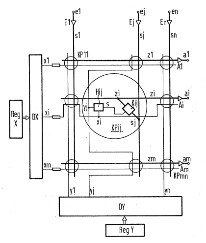
1. A broadband signals switching matrix network having a
cross-point matrix in FET technology, whose inputs, ej-sj, can
each be respectively provided with an input driver circuit, Ej,
and whose outputs, zi-ai, can each respectively be provided
with an output amplifier circuit, Ai, and whose switching ele-
ments, Kij, respectively controlled by a holding memory cell,
Hij, are respectively formed with a series circuit of a switch-
ing transistor, Tk, whose control electrode is charged with a
through-connect signal or an inhibit signal and of an input
transistor, Te, that has its control electrode connected to the
appertaining matrix input line, sj, said series circuit having
the main electrode of one of the transistors, Tk or Te, that is
connected opposite from the series circuit, connected to the
appertaining matrix output line, zi, the matrix output line,
zi, being connected to a pre-charging potential source, UDD,
via a pre-charging circuit, Tipc, that has an unlocking input
connected to a clock signal line, TPC, having a pre-charging
clock signal that defines a pre-charging phase, pv, of a bit
through-connect time span subdivided into the pre-charging
phase, pv, and into a remaining bit through-connect time span,
so that the matrix output line, zi, is charged to a pre-
charging potential in every pre-charging phase, pv, comprising
a main electrode of the other transistor of the transistors, Te
or Tk, that is connected opposite the series circuit, continu-
ously connected to a terminal, USS, of an operating voltage
source.


2. The broadband signal switching matrix network
according to claim 1, wherein a main electrode of the
other transistor of the transistors, Te or Tk, that is
connected opposite the series circuit, is connected to
one terminal, USS, of the operating voltage source via a
further transistor, Tai, individually associated to the
matrix output line that has its control electrode
connected to the output, ai, of an output amplifier
circuit, Ai, that is individually associated to the
matrix output line.


3. The broadband signals switching matrix network
according to claim 1, wherein the transistor series
circuit, Tk-Te, of every switching element, Kij, has its
switching transistor, Tk, connected to the matrix output
line, zi.


4. The broadband signal switching matrix network
according to claim 1, wherein the transistor series
circuit, Tk-Te, of every switching element, Kij, has its
input transistor, Te, connected to the matrix output
line, zi.


5. A broadband signals switching matrix network
having a cross-point matrix in FET technology, whose
inputs, ej-sj, are each respectively provided with an
input driver circuit, Ej, and whose outputs, zi-ai, are
each respectively provided with an output amplifier
circuit, Ai, and whose switching elements, Kij,
respectively controlled by a holding memory cell, Hij,


16


are respectively formed with a series circuit of a
switching transistor, Tk, whose control electrode is
charged with a through-connect signal or an inhibit
signal and of an input transistor, Te, that has its
control electrode connected to the appertaining matrix
input line, sj, said series circuit having the main
electrode of one of the transistors, Tk or Te, that is
connected opposite from the series circuit, connected to
the appertaining matrix output line, zi, whereby the
matrix output line, zi, is connected to a pre-charging
potential source, UDD, via a pre-charging circuit, Tipc,
that has an unlocking input connected to a clock signal
line, TPC; having a pre-charging clock signal that
defines a pre-charging phase, pv, of a bit through-
connect time span subdivided into the pre-charging phase,
pv, and into a remaining bit through-connect time span,
so that the matrix output line, zi, is charged to a pre-
charging potential in every pre-charging phase, pv,
comprising a main electrode of the other transistor of
the transistors, Te or Tk, that is connected opposite the
series circuit, continuously connected to a terminal,
USS, of an operating voltage source, a main electrode of
the other transistor of the transistors, Te or Tk, that
is connected opposite the series circuit, connected to
one terminal, USS, of the operating voltage source via a
further transistor, Tai, individually associated to the
matrix output line that has its control electrode
connected to the output, ai, of an output amplifier
circuit, Ai, that is individually associated to the
matrix output line, the transistor series circuit, Tk-

17


Te, of every switching element, Kij, having its switching
transistor, Tk, connected to the matrix output line, zi.


6. A broadband signals switching matrix network
having a cross-point matrix in FET technology, whose
inputs, ej-sj, are each respectively provided with an
input driver circuit, Ej, and whose outputs, zi-ai, are
each respectively provided with an output amplifier
circuit, Ai, and whose switching elements, Kij,
respectively controlled by a holding memory cell, Hij,
are respectively formed with a series circuit of a
switching transistor, Tk, whose control electrode is
charged with a through-connect signal or an inhibit
signal and of an input transistor, Te, that has its
control electrode connected to the appertaining matrix
input line, sj, said series circuit having the main
electrode of one of the transistors, Tk or Te, that is
connected opposite from the series circuit, connected to
the appertaining matrix output line, zi, whereby the
matrix output line, zi, is connected to a pre-charging
potential source, UDD, via a pre-charging circuit, Tipc,
that has an unlocking input connected to a clock signal
line, TPC, having a pre-charging clock signal that
defines a pre-charging phase, pv, of a bit through-
connect time span subdivided into the pre-charging phase,
pv, and into a remaining bit through-connect time span,
so that the matrix output line, zi, is charged to a pre-
charging potential in every pre-charging phase, pv,
comprising a main electrode of the other transistor of
the transistors, Te or Tk, that is connected opposite the


18


series circuit, continuously connected to a terminal,
USS, of an operating voltage source, a main electrode of
the other transistor of the transistors, Te or Tk, that
is connected opposite the series circuit, connected to
one terminal, USS, of the operating voltage source via a
further transistor, Tai, individually associated to the
matrix output line that has its control electrode
connected to the output, ai, of an output amplifier
circuit, Ai, that is individually associated to the
matrix output line, the transistor series circuit, Tk-
Te, of every switching element, Kij, having its input
transistor, Te, connected to the matrix output line, zi.


19

Description

Note: Descriptions are shown in the official language in which they were submitted.


1 330232
, '
BACKGROUN~ OF ~n~ LEy___ION
~ oderndevelopments in telecommunications technology
have lead to integrated services communications
transmission and switching systems for narrow band and
broadband communications services that have light
waveguides in the region of the subscriber lines as a
transmission medium. The light waveguides provide both
narrow band communications services such as, in
particular, 64 kbit/s digital telephony as well as
broadband communications services such as, in particular,
140 Mbit/s picture telephone. As a result narrow band
signal switching matrix networks and broadband signals
switching matrix networks (preferably having shared
control equipment) can also be provided side-by-side in
the switching centers (see German Patent 24 21 002).
A known broadband signal switching matrix network
(see, for example, European Patent Al 0 262 479) has a
cross-point matrix in FET technology whose switching
elements are each formed with a switching transistor that
has its control electrode charged with a through-connect
or inhibit signal and has its main electrode connected
to the appertaining matrix output line. The switching
elements each have a series transistor forming a series
circuit with the switching transistor. This series
transistor has its control electrode connected t ~ _he
appertaining matrix input line and its main electrode
connected opposite from the series circuit being
connected via a sampling transistor to one terminal of
an operating voltage source to whose other terminal the
respective matrix output line is connected via a pre~


1 330232

charging transistor. The pre-charging transistor and
sampling transistor are respectively charged oppositely
from one another at their control electrode with a
switching matrix network selection clock that subdivides
a bit through-connect time span into a pre-charging phase
and into the actual through-connection phase. As a
result the matrix output line, for an inhibited sampling
transistor, is at least approximately charged in every
preliminary phase to the potential at the other terminal
of the operating voltage source.
This known broadband signal switching matrix network
that can have sampling transistors individually
associated to the switching elements or sampling
transistors, which are individually associated to the
matrix input line or matrix output line, requires
separate clock lines that run through the cross-point
matrix for selecting these sampling transistors. This
requires a circuit surface space requirement and involves
a corresponding capacitative load on the matrix output
lines. In order to guarantee adequate protection against
signal interference, clock distribution and couplings
between matrix input lines and matrix output lines
require adequately high signal amplitudes on the matrix
output lines, this involving a relatively high power
consumption.
SUMMARY OF THE INVENTION
An object of the present invention is to provide a
broadband signal switching matrix network having limited
dissipated power given adequate prbtection against
disruption in which such disadvantages are avoided.


` 1 330232

The present invention is directed to a broadband
signal switching matrix network having a cro~s-point
matrix ET technology whose inputs can each be provided
with an input driver circuit, ~rhose outputs can each be
provided with an output amplifier circuit, and each of
whose switching elements controlled by a holding memory
cell is respectively formed with a series circuit of a
switching transistor whose control electrode is charged
with a through-connect signal or inhibit signal and an
input transistor that has its control electrode connected
to the appertaining matrix input line. The series
circuit has the main electrode of one transistor, that
is connected opposite from the series circuit, connected
to the appertaining matrix output line, -~ rdbr the
matrix output line~q~ connected to a pre-charging
potential source via a pre-charging circuit that has an
unlocking input connected to the clock signal line of a
pre-charging clock signal that defines the pre-charging
phase of a bit through-connect time span that is
subdivided into such a pre-charging phase and into the
: ~.
remaining bit through-connection time span. As a result
the matrix output line is charged to a pre-charging
potential in every pre-charging phase. This broadband
switching matrix network is inventively characterized in
that the main electrode of the other transistor that is
connected opposite from the series circuit is
continuously connected to a terminal of the operating
voltage source.
In addition to providing the advantage of avoiding
additional clock lines and, potentially, of being able


.

; ~ ~
-~
1 330232

to co-utilize the operating voltage supply of the cross-
point-associated holding memory cell already required for
the feed of the switching element controlled by this
holding memory cell, the present invention provides the
further advantage that the output line can be operated
with a very small signal boost of, for example, 1 V for
an operating voltage of, for example, 5 V. This
producing a corresponding reduction in the dissipated
powers. At the same time, the possible reduction of
signal boost on the matrix output line also produces a
reduction of disturbances of the opexating voltage of the
broadband signal switching matrix network that are caused

by power peaks.
.
In a further development of the present invention,
the maln electrode of the other transistor, that is
connected opposite from the series circuit, can be
connected to the one terminal of the operating voltage
source via a transistor individually associated to the
matrix output line that has its control electrode
connected to the output of an output amplifier oircuit
that is individually associated to the matrix output
line. Given a corresponding change in signal status at
the output of the output amplifier circuit, the
transistor individually associated to the matrix output
line is thereby inhibited, so that a further charge
reversal of the output line is avoided and the signal
boost is thus limited.
In a further development of the present invention,

the transistor series circuit of each and every switching
element can have its input transistor connected to the
"'


1 330232

matrix output line.
Alternatively thereto, however, it is possible that,
in a further development of the present invention, the
transistor series circuit of each and every switching
element has its switching transistor connected to the
matrix output line, this avoiding a capacitative loading
of the matrix output line by the channel capacitance of
the series transistors of switching elements that are not
through-connected.
BRIEF DESCRIPTION OF THE DRAWINGS
The features of the present invention which are
believed to be novel, are set forth with particularity
in the appended claims. The invention, together with
further objects and advantages, may best be understood
by reference to the following description taken in
conjunction with the accompanying drawings, in the
; several Figures in which like reference numerals identify
like elements, and in which~
Figure 1 is a schematic of a broadband switching
matrix network;
~; Figures 2-6 are circuit schematics of circuit-
oriented details of the present invention; and -~
Figure 7 is a graph depicting signal statuses.
DESCRIPTION OF THE PREFERRED EMBODIMENT
Figure 1 schematically depicts a broadband signal
switching matrix network in a scope required for an
understanding of the present invention. Input driver j~
circuits El...Ej... En are provided at the input
el...ej...en thereof that connect to column lines
sl...sj...sn of a cross-point matrix and the outputs

33023~

row
al...ai...am thereof reached by ~r~ lines zl...zi...zm
of the cross-point matrix are provided with output
amplifier circuits Al...Ai...Am.
The cross-point matrix has cross-point~
KPll...KPij...KPmn whose switching element (as is
indicated in greater detail i~ the case of the cross-
point KPij for the switching element Kij thereof) can be
respectively driven by a cross-point associated holding
memory cell Hij (at the cross-point KPij) whose output
s connects to the control input of the respective
switching element (Kij at the cross-point KPij).
According to Figure 1, the holding memory
cells...Hij...are driven in two coordinates by two
selection decoders, namely, a row decoder DX and a column
decoder DY via corresponding selection lines
xl...xi...xm: yl...yj...yn.
As may be seen from Figure 1, the two selection
decoders DX, DY may thereby be chargeable, proceeding
from input registers ~ X, ~ Y, with a respective
cross-point row address or, respectively, cross-point
column address shared by a matrix line (row or column)
of cross-points. In response thereto they respectively
output a "1" selection signal to the selection line
corresponding to the respective cross-point line address.
The coincidence of a row selection signal "1" and of a
column selection signal "1" at the intersection of the
appertaining matrix row with the appertaining matrix
column during the set-up of a corresponding call then
effects an activation of the holding memory cell situated
there, for example, the memory cell Hij. This has the


:


1 330232
~ 20365-2~54
result that the swltchlng element controlled by the apper-
talnlng holding memory cell (Hl~) becomes conductlve, the .
swltchlng element Kl~ in the example.
So that the swltchlng element Kl~ under conslderatlon
ln the example ls again inhibited for a clear down of the
appertalnlng call, the selectlon decoder DX ls agaln charged
wlth the appertalnlng row address proceedlng from the lnput
reglster Reg X, so that the row decoder DX agaln outputs a row
selectlon signal "1" on its output llne xl. Simultaneously, -~
the column decoder DY, proceedlng from lts lnput reglster Reg
Y, ls charged, for example, wlth a dummy address or wlth the
address of a column of unconnected cross-polnts, so that lt ~ ~`
outputs a column selectlon slgnal "0" on its output llne y~
The colncldence of row selectlon slgnal "1" and column selec-
tlon slgnal "0" then effects the resettlng of the holdlng
memory cell Hl~, wlth the result that the swltchlng element Ki~
controlled by it is lnhlblted.
The holdlng memory cells...Hl~... can be fashloned ln
a known manner. Thus, the holding memory cells (as known, for
example, by European patent A 0 238 834 and also sketched ln
Figures 5 and 6) can be formed wlth an n-channel transistor Tnh
and two cross-coupled inverter circuits (CMOS inverter circuits
~ I ~
Tp' Tn'; Tp'', Tn'' in Figure 5~ n-MOS inverter circuits Tnl',
Tnl'~ Tnl'', Tn'' ln Flgure 6), whereby one lnverter circuit
has its lnput slde connected to the appertainlng decoder output
y~ of the one selectlon decoder vla the n-channel translstor
Tnh that ln turn has lts control electrode charged with the
output slgnal of the appertaining decoder output xl of the
other selection


~ ~ .

1 330232

decoder. One inverter circuit has its output side
connected to the control input s of the appertaining
switching element.
How the switching elements~..Kij...can be realized
in circuit-oriented terms is illustrated in Figures 2,
3 and 4; the switching elements...Kij...are each formed
with a series circuit of a switching transistor Tk that
has its control electrode charged with a through-connect
signal or inhibit signal proceeding from the holding
memory cell and of an input transistor Te that has its
control electrode connected to the appertaining matrix
input line sj. The series circuit has the main electrode
of the one transistor Tk (in Figure 3 and Figure 4) or
Te (in Figure 2), that is connected opposite from the
series circuit, connected to the àppertaining matrix
output line zi.
¦ The matrix output line zi is thcrcby connected via
a pre-charging circuit to a pre-charging potential ssurce
proceeding from which the matrix output line zi can be
charged to a pre-charging potential lying between the two
operating potentials or to one of the two operating
potentials itself. A pre-charging potential source for
a pre-charging potential lying between the two operating
potentials can, in particular, be formed in a
, ~
fundamentally known manner (see for example, European
Patent A O 249 837) with a feedback CMOS inverter via ~ ~
which the matrix output line, in a pre-charging phase of -
a bit through-connect time span, is at least
approximately charged to the potential corresponding to
the threshold of the inverter. By contrast thereto, the ~


g - ,;'
''

1 330232
20365-2954
matrlx output llne zl ln the e~emplary embodlments shown ln
Flgures 2-4 ls connected to one termlnal (Uss in Figure 27 UDD
ln Flgure 3, Figure 4) of the operating voltage source UDD-Uss
vla a pre-charglng clrcuit that, as may also be seen from
Flgures 2-4, is formed in a known fashion (see for example,
European Patent A 0 262 479) with a pre-charging translstor
Tipc that has lts control electrode connected to a pre-charglng
clock llne Tpc.

:~
The maln electrode of the other translstor Te (ln
. ., , ~ ~ ~
Flgure 3 and Flgure 4) or Tk (in Figure 2) that is connected
opposite from the series clrcuit is continuously - i.e. not
clock-controlled - conneated to the other termlnal Uss, ground
(in Flgure 3 and Flgure 4) or UDD (in Flgure 2) of the opera-
tlng voltage source, to whlch end, glven dlrect connectlon
accordlng to Figure 2 and Figure 3, the correspondlng operatlng
voltage terminal (Uss, ground or, UDD ln Flgure 5 and Flgure 6)
of the cross-polnt-associated holdlng memory cell Hl~ (in
. -

Flgure 1, Figure 5 and Flgure 6) can be utlllzed. As a result ~
- , . -
the operatlng voltage supply o~ the cross-polnt-assoclated
holdlng memory cell that ls already requlred can be co-utillzed
for feedlng the swltchlng element controlled by thls holdlng
memory cell. In the exemplary embodiment of Figure 4, the maln
electrode of the other translstor (Te), that ls connectad oppo-
slte from the serles clrcuit, ls connected to the other terml-
nal Uss of the operatlng voltage source vla a translstor Tal
lndlvldually assoclated to the matrlx output llne that has lts
control electrode connected to the output al of an output
ampllfier clrcult Al that ls lndlvldually assoclated to the
matrlx output line. Glven a corresponding change of slgnal
30 status at the output ai of the output ampllfler circult Al, the
transistor Tai indlvldually assoclated to the matrlx outpu~


1 0 " ,,

1 330232
20365-2954
line ls thereby lnhibited, so that a further charge reversal of
the output llne ls avolded and the slgnal boost ls thus limi~
ted. : :~
As may be seen from Flgure 2, the translstor serles
circuit Tk-Te of every swltchlng element Kl~ can have lts lnput
transls~or Te connected to the matrlx output llne zl. Then, as
seen proceedlng from the matrlx output llne zl, the lnput tran~
slstor Te ls, ln a sense, transparent, so that changes ln slg- ~- -
nal status on the matrlx lnput llne s~ are transmltted vla the - -
channel capacltance of the lnput translstor Te onto the matrlx
output llne Zl even when the cross-polnt Kl~ ls lnhlblted.
Thls transmisslon can be avoided when the sequence of lnput
translstor Te and swltchlng translstor Tk ls interchanged in
the translstor serles circult Tk; Te of every swltchlng element
Ki~. As may also be seen from Flgure 3 an~ from Figure 4, the
transistor serles clrcuit Tk-Te of every switching element Ki~
then has lts swltching transistor Tk connected to the matrlx

. ~ . .
output line zl.
Preferably, n-channel translstors will be utllized as
the clrcuit transistors. Accordingly, the transistors in the
exemplary embodiments of Figures 2 and 4 are all of the n-
channel type, whereas the transistors (Te, Tk) provided in the
switching element...Ki~... in the exemplary embodiment of
Flgure 3 are of the n-channel type and the pre-charglng tran- `
sistors (Tipc) are of the p-channel type.
A corresponding pre-charging clock signal TpC that
charges the control electrode o~ every pre-charglng transistor
tTipc) effects that every pre-charging translstor (Tlpc) ls
transmlsslve ln every pre-charglng phase pv (ln Figure 7) of a
bit period that is subdivlded by the pre-charglng clock slgnal

lnto such a pre-charglng phase pv and lnto the remalning bl~
:" ':

11 `
~r :

1 330232
20365-2g54 -
through-connect tlme span (ph in Figure 7). As a result the
matrlx output llnes.~.zl... are at least approximately charged ~;
(durlng the pre-pha e pv) to the respectlve operatlng potential
(Uss ln Flgure 2~ UDD ln Flgure 3 and Figure 4) vla the resp~c~
tlve pre-charglng translstor ~Tipc ln Figures 2-4). Such a
pre-charglng clock signal for the exemplary embodlments o~
Flgures 2 and 3 ls shown ln Flgure 7 in llne Tpc; the inverted
pre-charglng clock slgnal ls used for the exemplary embodlment
of Flgure 4. ;~
In the followlng maln phase, ph (see Flgure 7
bottom), the pre-charglng translstors Tlpc (ln Flgures 2-4) are
lnhlblted ln the example by a "HIGH" pre-charglng clock slgnal
TPC (see Flgure 7, llne Tpc). When, ln a swltchlng element
Kl~, its swltchlng translstor Tk (ln Figures 2-4), whlch ls
preferably an n-channel translstor, ls transmlsslve as a con-
sequence of a through-connect slgnal ~ln the example, "HIGH"~
see Flgure 7, line s) received at lts control lnput s, and
when, accordlngly, the cross-polnt ls ln lts through-connect
condltlon, the matrlx output llne (row llne) zi connected to a
matrlx lnput line (column llne)...s~...via the assoclated
swltchlng element Kl~ wlll be dlscharged or wlll remaln at the
opèratlng potential assumed in the pre-phase pv,

.


12

, ,

;-~ 1330232


dependent on the signal status that corresponds to the
bit to be through-connected and that prevails on the
appertaining matrix input line ~column line)...sj....
When the "LOW" signal ~;tatus prevails on the
appertaining matrix input line (column line) sj, as
indicated with a broken line in Figure 7, line sj, and
when, accordingly, the (n-channel) input transistor Te
(in Figures 2-43 of the appertaining switching element
Kij is inhibited, then the appertaining matrix output
line (row line) zi is not discharged via this switching
element Kij. Rather, it retains the pre-charging
potential condition (Uss in the exemplary embodiment of
Figure 2; U~D in the exemplary embodiments of Figures 3
and 4) under the condition that no other cross-point
connected to this matrix output line (row line) zi is
situated in the through-connect condition.
When, by contrast, the "HIGH" signal status prevails
on the matrix input line (Column line) sj now under
consideration, as indicated with a solid line in Figure
7, line~ sj, and when, accordingly the input transistor
Te (in Figures 2-4) of the switching element Rij under
consideration is conductive, as is the switching

. ~ :
transistor Tk, then the matrix output line (row line) zi
is discharged via this switching element Kij and is drawn
to the compl:imentary operating potential (U~ in the
exemplary embodiment of Figure 2; Uss in the exemplary
embodiments o~ Figures 3 and 4).
The respective input signal is thus through-
connected and inverted via a cross-point unlocked

proceeding from its control input s.


13 `~


:: .

1 330232

The invention is not limited to the particular ~.
details of the apparatus depicted and other modifications
and applications are contemplated. Certain other changes ;~
may be made in the above described apparatus without
departing from the true spirit and scope of the invention
herein involved. It is intended, therefore, that the
subject matter in the above depiction shall be
interpreted as illustrative and not in a limiting sense.
.' ,:


,~ .

', .


14

Representative Drawing
A single figure which represents the drawing illustrating the invention.
Administrative Status

For a clearer understanding of the status of the application/patent presented on this page, the site Disclaimer , as well as the definitions for Patent , Administrative Status , Maintenance Fee  and Payment History  should be consulted.

Administrative Status

Title Date
Forecasted Issue Date 1994-06-14
(22) Filed 1989-08-04
(45) Issued 1994-06-14
Deemed Expired 2001-06-14

Abandonment History

There is no abandonment history.

Payment History

Fee Type Anniversary Year Due Date Amount Paid Paid Date
Application Fee $0.00 1989-08-04
Registration of a document - section 124 $0.00 1989-11-17
Maintenance Fee - Patent - Old Act 2 1996-06-14 $100.00 1996-05-23
Maintenance Fee - Patent - Old Act 3 1997-06-16 $100.00 1997-05-14
Maintenance Fee - Patent - Old Act 4 1998-06-15 $100.00 1998-05-28
Maintenance Fee - Patent - Old Act 5 1999-06-14 $150.00 1999-05-13
Owners on Record

Note: Records showing the ownership history in alphabetical order.

Current Owners on Record
SIEMENS AKTIENGESELLSCHAFT
Past Owners on Record
TRUMPP, GERHARD
WOLKENHAUER, JAN
Past Owners that do not appear in the "Owners on Record" listing will appear in other documentation within the application.
Documents

To view selected files, please enter reCAPTCHA code :


To view images, click a link in the Document Description column. To download the documents, select one or more checkboxes in the first column and then click the "Download Selected in PDF format (Zip Archive)" or the "Download Selected as Single PDF" button.

List of published and non-published patent-specific documents on the CPD .

If you have any difficulty accessing content, you can call the Client Service Centre at 1-866-997-1936 or send them an e-mail at CIPO Client Service Centre.


Document
Description 
Date
(yyyy-mm-dd) 
Number of pages   Size of Image (KB) 
Drawings 1995-09-07 3 173
Claims 1995-09-07 5 227
Abstract 1995-09-07 1 40
Cover Page 1995-09-07 1 77
Representative Drawing 2001-02-02 1 16
Description 1995-09-07 13 677
Prosecution Correspondence 1994-01-05 1 39
Examiner Requisition 1992-04-21 1 59
Prosecution Correspondence 1992-07-28 6 280
PCT Correspondence 1994-03-29 1 30
Fees 1997-05-14 1 81
Fees 1996-05-23 1 62