Note: Descriptions are shown in the official language in which they were submitted.
1330~90 :
SPECIFICATION ~
':
TITLE OF THE INVENTION
Apparatus With An Inverse Nyquist Filter For ~ ~:
Processing Vestigial Multiplex Signals In -
Quadrature :
BACKGROUND OF THE INVENTION
1 Field of the Invention
This invention relates to an apparatus for multiplexing
a specific signal with an amplitude-modulated signal,
transmitting and receiving the multiplexed signal, and
extracting the specific signal from the multiplexed signal.
,.~.
2. Descri~tion of the Prior Art -
In Japan, more than 25 years have passed since the ~-
color television broadcasting of the current NTSC (National
Television System Committee) system began in 1960. In this
period, to answer the requests for a finer definition and .
higher performance television receiver, various new televi-
sion systems have been proposed. At the same time, the
contents of the programs presented to the viewers have been
changed ~rom the mere studio programs or location programs
'~
--1-- .
. .
1 33 ~3 ~ D : ~
~ ~,
to programs providing images of higher picture quality and ;~
higher realistic feeling such as cinema-size movies.
The current broadcasting is specified with 525 scanning
lines, 2:1 interlace scanning, a luminance signal horizontal
bandwidth of 4.2 MHz, and an aspect ratio of 4:3 (see, for
example, Broadcasting Technology Series, Color Television,
ed. by Japan Broadcasting Corporation, Japan Broadcasting
Corporation Pub., 1961). In this background, several
television signal composition methods aiming at compatibility
with the current broadcasting system and enhancement of
horizontal resolution have been proposed. One of such
examples is disclosed in the Japanese Laid-Open Patent No.
59-171387. Considering the NTSC television signal expressed
on a two-dimensional~plane of temporal frequency f1 and
vertical frequency f2, chrominance signals C are present in
the second and fourth guadrants due to the phase relationship
with the chrominance subcarrier fsc. The example uses the
vacant first and third quadrants for multiplexing the high
frequency components of the luminance signal. The chromi-
nance signal and the multiplexed high frequency components
are separated and reproduced at the receiving end, thereby
enhancing the horizontal resolution.
--2--
13303~0 ~ ~
In the current television broadcast, as is clear from
the description above, the band of signals is limited by the
standard, and it is not easy to add some new information in
quantity. For example, methods to enhance the horizontal
resolution are proposed, but many problems are left unsolved
from the viewpoint of the compatibility with the current
television broadcasting and the deterioration of demodulation
characteristics of high frequency components in a moving
picture. Besides, from the standpoint of effective use of
the radio wave resources, the transmission band cannot be
extended as an easy solution.
SUMMARY OF THE INVENTION
It is a primary;~object of this invention to present a
multiplex signal processing apparatus for multiplex trans- ~-
mission of a large quantity of information in a defined
band.
According to this invention, a multiplex signal proces-
sor at a transmitter side amplitude-modulates a main carrier
by a main signal to obtain a vestigial sideband (VSB),
modulated main signal; amplitude-modulates a carrier which
.. : ... .. ..... . . . .
has the same frequency as but is shifted in phase by 90
-3-
.' .
1330a~0 ~
from the main carrier by a specific multiplex signal to
obtain a double sideband, modulated multiplex signal; passes
the double sideband, modulated multiplex signal through a
Nyquist filter to obtain a vestigial sideband (VSB),
modulated multiplex signal; and superposes the VSB,
modulated multiplex signal on the VSB, modulated main signal
to obtain a multiplexed signal, which is transmitted.
A multiplex signal processor at a receiver side has a
synchronous detector and a ~uadrature distortion eliminating
filter for demodulating the main and multiplex signals from
the received multiplexed signal.
By this constitution, in, for example, television
broadcasting, it is possible to obtain not only the conven-
tional television br~oadcasting images but also multiplex
information at the receiver, by generating a television
signal capable of multiplex transmission of other information
within the standard band of the existing television broad-
casting. At the same time, when received the multiplexed
signal by an existing television receiver, there is almost
no interference by the multiplex signal, and the compatibil-
ity with the existing television receivers can be maintained.
...
Further, since multiplex transmission of other information
is possible in a band determined by the standard, it is very
,~
i
~ --4--
133~0 ~
advantageous also from the viewpoint of effective use of
radio wave resources.
BRIEF DESCRIPTION OF THE DRAWINGS
yig. 2, Fig. 5(a), Fig. 6(a), Fig. 9(a), Figs. 12(a),
Fig. 18, Fig. 24, and Fig; 30 are block diagrams each
showing a multiplex signal processor at the transmission
side embodying this invention;
Fig. 4(c), Fig. 5(b), Fig. 6(b), Fig. 9(b), Fig. 12(b),
Fig. 25, and Fig. 35 are block diagrams each showing a
multiplex signal processor at the reception side embodying
this invention; ;
Figs. l(a)-(c), Figs. 7(a)-(n), Figs. 10(a)-(j), and
Figs. 23(a)-(f) are spectral diagrams showing the processing
method of the multiplex signal processor at the transmission
side according to this invention;
Fig. 4(a), Figs. 8(a)-(n~, and Fig~s. ll(a)-(u) are
special diagrams showing the processing method of the
multiplex signal processor at the reception side according
to this invention;
Fig. 4(b) is a vector diagram used to explain the
principle of the multiplex signal processor at the reception
side according to this invention;
--5--
;?
:i,
, . . .
13~90
Figs. 3(a), (b), and (c) are respectively a block
diagram, spectral diagram and vector diagram showing a
conventional television receiver;
Fig. 13(a) is an internal circuit composition of a
signa,l generator 125 in Fig. 12(a);
Fig. 13(b) shows an example of a discriminating signal;
Fig. 14 is a internal circuit composition of the signal
separator 131 shown in Fig. 12(b);
Fig. 15 is an internal circuit composition of the
signal selector 137 shown in Fig. 12(b);
Fig. 16(a) is an example of a display screen of an
existing television and Fig. 16(b) is a time-axis expression
of a composite video signal;
Fig. 17(a) is a~n example of a display screen at aspect
ratio of 5:3 and Figs. 17(b)-(c) are time-axis expressions
of a composite video signal;
Fig. 19 is a picture composition a~t different aspect
ratio;
Figs. 20(a)-(e) are signal waveform diagrams showing
the signal processing step in Fig. 18;
Figs. 21(a)-(e) are spectral diagrams showing the
..... .... - - -, -
- signal processing step in Fig. 18;
-6-
~'
1330~)9
':
Fig. 22 is a diagram showing the blanking period of a
television signal;
Fig. 26 is a block diagram of a transmission device
according to this invention;
Figs. 27(a)-(d) show waveforms of a reference signal
generated in the reference signal generator shown in Fig. 26 ~'
and Fig. 28;
Fig. 28 is a circuit composition of an example of the
ghost reduction device of Fig. 26;
Fig. 29 is a circuit composition of an example of the
transversal filter of Fig. 28;
Fig. 31 is a circuit composition of an example of video
high frequency range auxiliary signal circuit of Fig. 30;
Fig. 32 is a cir~cuit composition ~of an example of wide
aspect video auxiliary circuit of Fig. 30;
Figs. 33(a)-(c) are waveform diagrams used to explain
the operation of wide aspect video auxi~iary circuit of Fig.
30; ;
Fig. 34 is a circuit composition of an example of the
scramble processor of Fig. 30;
Fig. 36 is a circuit composition of an example of the ;-
video high frequency range addition circuit of Fig. 35;
Fig. 37 is a circuit composition of an example of the
wide a~pect video addition circuit of Fig. 35;
,
x~
:
133~a90
Fig. 38 is a circuit composition of an example of the
scramble demodulator of Fig. 35;
Fig. 39 is a circuit composition of an example of the
small screen video addition circuit of Fig. 35; and
Figs. 40(a)-(c) are waveform diagrams used to explain
the operation of the sm~li screen video addition circuit of
Fig. 35.
Fig. 41 is a block diagram showing a television multi-
plex signal processor at the transmission side according to
this invention;
Fig. 42 is a circuit composition of an example of the
multiplex signal processing circuit 6l0 shown in Fig. 41;
Fig. 43 is a block diagram showing a television multi-
plex signal processor~ at the reception~side according to
this invention; and
Fig. 44 is a circuit composition of an example of the
multiplex signal regenerating circuit 7~01 shown in Fig. 43.
DETAILED DESCRIPTION OF THE PREFERRED EMBODIMENTS
Figs. l(a)-(c) are spectral diagrams used to show the
television signal processing method at the transmission side
,. ..
according to an embodiment of this invention. More specifi-
cally, Fig. l(a) is a spectral diagram of a vestigial
~ ;-8-
1330~90
sideband, amplitude-modulated television signal in the NTSC
television system, in which the lower sideband of video
carrier Pl is the vestigial sideband. In this case, the
signal may be any television signal amplitude-modulated in
the vestigial sideband, and it is not limited to the NTSC
.
television signal. Fig, itb) is a signal which is obtained
by amplitude-modulating a vestigial sideband of a carrier P2
which has the same frequency but is different in phase by , ~`
90 from the video carrier Pl by a multiplex signal
different from,the television signal shown in Fig. l(a).
Preferably the carrier P2 is removed in the blanking period.
When the signal shown in Fig. l(b) is multiplexed with the
television signal shown in Fig. l(a), the result is as shown
in Fig. l~c). The multiplex signal ma;y be either an analog
signal or a digital signal.
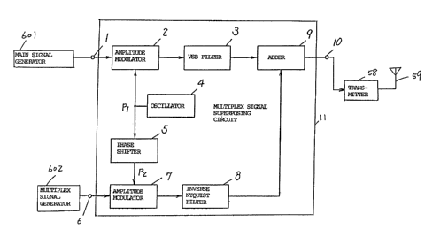
Fig. 2 i a block diagram showing a television multiplex
signal processor at the transmission s~de as one of the
embodiments of this invention, in which element 601 is a
main signal generator; element 1 is a main signal input
.~
terminal; element 2 is an amplitude modulator; element 3 is
a VSB filter; element 4 is an oscillator; element 5 is a
phase shifter; element 602 is a multiplex signal generator;
element 6 is a multiplex signal input terminal; element 7 is
_ g _
1, .
1330590 ~:
an amplitude modulator; element 8 is an inverse Nyquist
filter; element 9 is an adder; element 10 is a composite
signal output terminal; element 58 is a transmitter, and
element 59 is an antenna. Numeral 11 denotes a multiplex
signal superposing circuit. By a main signal generated by
the original signal generator 601, for example, a video
baseband signal, a carrier P1 generated by the oscillator 4
is amplitude-modulated by the amplitude modulator 2. The
modulated signal is band limited by the VSB filter 3 to
become a vestigial sideband signal, which is fed to the ;
adder 9. The VSB filter 3 is a filter to transform a double
sideband signal into a vestigial sideband signal. The
carrier P1 from the oscillator 4 is shifted in phase by 90
by the phase shifter;~5 to form carrier,P2. By a multiplex
signal generated in the multiplex signal generator 602, the
carrier P2 is amplitude-modulated to have a double sideband
by the amplitude modulator 7, and prefeFably in the blanking
period the carrier is removed. The phase shift direction of
the phase shifter 5 may be either fixed or varied at inter-
vals of the horizontal scanning period, field or frame. The
modulated multiplex signal is band limited by the inverse -~
Nyquist filter 8, and then fed to the adder 9.
The amplitude frequency characteristic of the inverse
Nyquist filter 8 is, as mentioned later, to possess a -
10-
1330~90
property symmetrical to the amplitude frequency characteris-
tic immediately before video detection by the receiver with
respect to the video carrier. The output of the adder 9 is
a composite signal. That is, the modulated multiplex signal
is superposed on the modulated video baseband signal by the
adder 9 to produce the composite signal. The composite
signal is transmitted from the transmitter 58 with the
antenna 59, but the transmission path is not limited to a
wireless system. In this example, the composite signal is
obtained by adding the outputs of the VSB filter 3 and the ~
inverse Nyguist filter 8, but is is also possible to feed ~-
the sum of the outputs of the amplitude modulator 2 and the ~ 4
inverse Nyquist filter 8 into the VSB filter 3 to obtain the --~
composite signal.
On the other hand, a television multiplex signaI
processor at the reception side as one of the embodiments of
this invention is as follows. The foll~wing example refers
to terrestrial broadcasting of an NTSC television system,
but it is not intended as a limitation thereof. Fig. 3(a)
is a block diagram of an existing television receiver for
video synchronous detection, in which element 21 is an -~
antenna; element 22 is a tuner; element 23 is a Nyquist
filter; element 24 is a video detector; element 25 is a
1 33~5~0
carrier regenerator, and element 26 is a main signal output
terminal. The signal transmitted from the transmission side
is received by the antenna 21, converted in frequency to an
intermediate frequency band by the tuner 22, and band
limited by the Nyquist filter 23. The band-limited signal
is fed into the video detector 24 and the carrier regenerator
25. In the carrier regenerator 25, a video carrier Il for
synchronous detection is regenerated. The band-limited
signal is synchronously detected by the carrier Il by the
video detector 24, and becomes the main signal, that is, the
video baseband signal. The frequency characteristic of the
Nyquist filter 23 is as follows. Referring to Fig. 3(b)
which shows the frequency characteristic of the Nyquist
filter 23, the ampli$ude is attenuated by 6 dB at the video
carrier Il, and the Nyquist filter characteristic possesses
nearly an odd-symmetrical amplitude property with respect to
the video carrier Il.
On the other hand, as shown in Fig. l(b), when the
multiplex signal is band limited by the filter in the
transmitter having an inverse characteristic to the frequency
characteristic of the Nyquist filter in the receiver, the
multiplex signal components in the shaded area of Fig. 3(b)
is nearly a double sideband. When this is expressed by a
-12-
1330~90 ~
vector diagram, it becomes as shown in Fig. 3(ci, in which
I1 is the video carrier of the main signal, that is, the ~
video baseband signal, and I2 is the carrier of the multiplex ~-
signal in which the carrier has the same frequency but is ;
different in phase by 90~ from I1. The video baseband
signal is a vestigial sideband with respect to the carrier -
I1, so that the upper and lower sidebands are vector aU and
vector aL, respectively, which are vector a1 and vector a2,
respectively, when decomposed into orthogonal vectors.
Since the multiplex signal is nearly a double sideband
signal, supposing the upper and lower sidebands to be vector
bU and vector bL, respectively, their synthetic vector.is
b2, which is the only component to intersect with the vector
I1 orthogonally. That is, when the main signal is synchro-
nously detected by the carrier I1, quadrature distortion due
to the vector a2, and vector b2 components does not occur.
Thus, the impairment by the multiplex signal to the existing
television receiv~r performing video synchronous detection
does not occur, in principle.
Next, the detection of the multiplex signal at the
reception side is described below. The signal of the video
intermediate frequency band which is the output of the tuner
1 3 3 ~
is band limited by a band-pass filter, as shown in Fig.
4(a), so that the main signal, that is, the video baseband
signal becomes a double sideband signal. Its vector expres-
sion is shown in Fig. 4(b). Since the multiplex signal is
vestigial sideband with respect to the carrier I2, the upper
and lower sidebands are vector bU and vector bL, respective-
ly, which become vector b1 and vector b2, respectively, when
decomposed into orthogonal vectors. At the same time, since
the video baseband signal is made into nearly a double
sideband signal by the function of the band-pass filter,
supposing the upper. and lower sidebands to be vector aU and
vector aL, respectively, their synthetic vector is a1, which
is the only component intersecting orthogonally with the .
vector I2. That is,~when the multiplex signal is synchro-
nously detected by the carrier I2, quadrature distortion due ..
to the vector a1, and vector b1 components does not occur.
Thus, only the multiplex signal components can be demodulated.
Fig. 4(c) shows an example of television multiplex
signal processor for also demodulating the multiplex signal, . :
in which element 31 is an antenna; element 32 is a tuner; ~.
element 33 is a Nyquist filter; element 34 is.a video . ..
detector; element 35 is a carrier regenerator; element 36 is
-14-
l330~sa
an original signal output terminal; element 37 is a band-pass
filter; element 38 is a phase shifter; element 39 is a
multiplex signal detector; element 40 is a multiplex signal
output terminal; element 603 is a main signal processor, and
element 604 is a multiplex signal processor. Element 41
denotes a mult~plex signal separator. The multiplexed
signal transmitted from the transmission side is received by
the antenna 31, converted in frequency into the intermediate
frequency band by the tuner 32, and band limited by the
Nyquist filter,33. The band-limited signal is supplied into
the video detector 34 and the carrier regenerator 35. In
the carrier regenerator 35, a video carrier I1 for sy~chro-
nous detector is regenerated. The band-limited signal is
detected by the carrier I1 in the video detector 34, and
becomes the main signal, that is, the video baseband signal.
The main signal is converted into, for example, R, G, B
signals by the main signal processor 6~3, and is displayed ~;~
on a screen lOC0. ~-~
The output of the tuner 32 is band-limited also as
shown in Fig. 4(a~ by the band-pass filter 37. By a carrier
I2 obtained by 90 phase shifting in the carrier I1 by the
phase shifter 38 (that is, by the carrier I2 having the same
phase as the carrier for multiplex signal modulation used at
.
--15-
1330a9~
the transmission side), the band-limited signal synchronously
detected in the multiplex signal detector 39, and becomes
the multiplex signal. The multiplex signal is subjected to ;;
processing which is opposite to the processing by the -
multiplex signal generator at the transmission side, in the
multiplex signa regenerator 604. The video detector 34 and
the multiplex signal detector 39 are detectors for the
synchronous detection of an amplitude-modulated signal.
As described above, in the existing receiver, since the
multiplex signal is nearly cancelled by the synchronous
detection by the video carrier I1, the main signal is not
interfered with by the multiplex signal. Further, in the
receiver capable of demodulating the multiplex signal, nQt
only the main signalj that is, the video baseband signal is
obtained in the same way as above, but also the multiplex
signal can be also obtained without quadrature distortion by
filtering and synchronous detection by *he carrier I2. This
is not limited to the NTSC television system, and can be
applied to any system as long as the signal is amplitude-
modulated in the vestigial sideband.
Fig. 5(a) is a block diagram showing a television
multiplex signal processor at the transmission side for
multiplexing the high frecuency components of the luminance
-16-
1330~90
signal as one of the embodiments of this invention, in which
elements 51 are R, G, B input terminals; element 52 is a
matrix circuit; element 53 is a chrominance modulator; ~.
element 54 is a first filter; element 55 is a second filter;
element 57 is a frequency converter; element 56 is an adder;
element 11 is a multiplex signal superposing circuit;
element 1 is a main signal input terminal; element 6 is a
multiplex signal input terminal; element 10 is a composite r
signal output terminal; element 58 is a transmitter, and
element 59 is an antenna. R, G, B signals from a video
camera or the like.are supplied into the matrix circuit 52
to be converted into luminance signal Y and the chrominance
difference signals I and Q. The chrominance difference . :'
signals I and Q are ~odulated in the c~rominance modulator
43 to become a carrier chrominance signal, which is fed into
the adder 56. The luminance signal Y is fed into the first
filter 54 and the second filter 55. The high frequency
components of the luminance signal Y which are band limited ,
by the second filter 55 are converted into the low frequenc,,y
range by the frequency converter 57. The output of the
first filter 54 is added to the.carrier chrominance signal....
in the adder 56. The output of the adder 56 is fed through
the main signal input terminal 1 into the multiplex signal
.
. ,.
, -17-
133~0 ~:
superposing circuit 11. The output of the frequency convert-
er 57 is fed through the multiplex signal input terminal 6
into the multiplex signal superposing circuit 11. The
output of the multiplex signal superposing circuit 11 is a
composite television signal having high frequency components
of the luminance signal superposed on the video baseband
signal which is the main signal. The composite television
signal is fed through the composite signal output terminal
10 into the transmitter 58, and is transmitted from the
antenna 59. Here, the first filter is a low-pass filter
passing, for example, 4.2 MHz or lower, and the second
filter is a high-pass filter passing, for example, 4.2~MHz
or higher or a band-pass filter passing between, for example
4.2 and 5.2 MHz. ;~ ~
Fig. 5(b) is a block diagram showing a television
multiplex signal processor at the reception side for repro-
ducing the high frequency components o~ the luminance signal
as one of the embodiments of this invention, in which
element 41 is a multiplex signal separator; element 36 is a
main signal output terminal; element 40 is a multiple signal
output terminal; element 61 is a luminance-chrominance
separation circuit; element 62 is a frequency converter;
element 63 is an adder; element 64 is a chrominance demodu-
l~tor; eLement 65 is a matrix circuit, and elements 66 are
-18-
1330~90
R, G, B output terminals. As stated above, the main signal,
that is, the video baseband signal is outputted from the
multiplex signal separator 41 through the main signal output
terminal 36, and is fed into the luminance-chrominance
separation circuit 61. The multiplex signal is outputted
from the multiplex se~aEator 41 through the multiplex signal
output terminal 40, and is fed into the frequency converter
62. The video baseband signal is separated into the lumi~
nance signal and the carrier chrominance signal by the
luminance-chrominance separation circuit 61. The separated
carrier chrominance signal is demodulated into the chromi-
nance difference signals I and Q in the chrominance demodu-
lator 64, and they are fed into the matrix circuit 65. The
demodulated multiple~ signal from the separator 41, that is,
the high frequency components of the luminance signal, is
converted into the original f requency band by the f requency
converter 62, and is added to the low fLequency component of
the luminance signal separated by the luminance-chrominance
separation circuit 61 in the adder 63, and the added result
is fed into the matrix circuit 65. The outputs of the
matrix circuit 65 are R, G, B signals, which are supplied,
for example, into a CRT 1000. In this way, the high fre-
quency components of the luminance signal can be transmitted
--19--
1330590
.. . .
as the multiplex signal and demodulated, so that the hori-
zontal resolution of luminance can be enhanced.
Fig. 6(a) is a block diagram showing a television -
multiplex signal processor at the transmission side for
multiplexing the high frequency components of the luminance
signal in another embQd~ment of this invention. Figs. ~
7(a)-~n) are explanatory diagrams showing the signal wave- ~-
forms at the corresponding parts in Fig. 6(a). Fig. 6(b) is
a block diagram showing a television multiplex signal
processor at the reception side for reproducing the high
frequency components of the luminance signal in another
embodiment of this invention. Figs. 8(a)-(1) are explanatory
diagrams showing the signal waveforms at the corresponding
parts in Fig. 6(b). ~ t
First the signal synthesizing method at the transmission
side shown in Fig. 6(a) is explained. A luminance signal of
a wide band (for example: 0 to 6.6 MHz~) is sepaxated into ~-~
three frequency bands YL, YHl, YH2 by a frequency separator ~-
91, in which YL is a low frequency luminance signal of 0 to
4.2 MHZ, YHl is a first high frequency luminance signal of
4.2 to 5.4 MHZ, and YH2 is a second high frequency luminance
signal o~ 5. 4 to 6.6 MHz. On the other hand, chrominance
-20-
1.330~
difference signals I and Q are subjected to quadrature
modulation by a quadrature modulator 92 to form a carrier
chrominance signal in the same manner as in the ordinary
NTSC system. The thus obtained carrier chrominance signal
is added to the low frequency luminance signal YL in an
adder 95. The ,spectr,um of the added result is shown in Fig.
7(g), which is similar to an ordinary NTSC signal. The
second luminance signal YH2 (Fig. 7(d)) from 5.4 MHz to 6.6
MHz is multiplied by a signal of 1. 2 MHz to be converted
into frequency a signal of 4.2 MHz to 5.4 MHz (Fig. 7(e)) by
a frequency converter 93. This 1.2 MHz signal may be
selected at 1/3 of the subcarrier of the chrominance S3 gnal,
and its phase information may be transmitted separately.
This luminance signal converted into t,he lower frequency
band is added to the first high frequency luminance signal
YHl in an adder 94 (Fig. 7(f)), and the resultant luminance ;'~
signal is multiplied by a signal cos cc t of about 4. 2 MHz
in a frequency converter 96 to be converted into a further
~.~
low frequency band (Fig. 7(h)). The reference phase of the
signal cos cc t for frequency conversion is transmitted in
multiplexed form, for example, in the vertical blanking
period. The composite luminance signal converted into the
-21-
1330~90
further low frequency and the composite video signal of 4.2
MHz or less which is compatible with the ordinary NTSC
signal are subjected to quadrature modulation by amplitude
modulators 7 and 2 using video carriers sin vc t and cos
vc t, respectively. At this time, when the multiplex signal
of a bandwidth of 1 MHz modulated by the amplitude modulator
7 has its direct-current component suppressed, the carrier
suppression modulation is achieved as shown in Fig. 7(m),
which is very convenient as stated later. This signal
passes through an inverse Nyquist filter 8 having the
characteristic as shown in Fig. 7(m). The video signal -~
which is the main signal passes through a VSB filter 3-as
shown in Fig. 7(1). The outputs of the filters 8 and 3 are
synthesized in a synthesizer 97 to beclome a signal as shown
in Fig. 7(n). This synthetic signal, as compared with the
ordinary NTSC video signal amplitude-modulated in the
vestigial sideband, has a multiplex si~nal of about 1 MHz
(the luminance signal of 4.2 to 5.2 MHz and luminance signal
of 5.2 to 6.2 MHz) superposed in the vestigial sideband. By
controlling the synthesizer of Fig. 6(a), it may be also
possible to add the multiplex signal only to that portion of
the signal other than the synchronous signal of the original
-22-
l33a~so
television signal. In this case, as mentioned later, in a
video synchronous detector of the system to reproduce the
video carrier on the basis of the synchronous signal, there
is no deterioration of the characteristics due to superposi- -
tion of the multiplex signal, and an excellent reception
performance as in the.conventional method can be obtained. -
Incidentally, the phase of the signal cos cc t for frequency
conversion may be controlled so as to be inverted at inter-
vals of at lest the horizontal scanning period, field or
frame. This can be said not only for cos cc t, but also to
other signals used for frequency conversion.
Referring now to Fig. 6(b) and Figs. 8(a)-(l), the
television multiplex signal processor at the reception side
for reproducing the ~high freguency components of the lumi-
nance signal is described below.
The received synthetic modulated signal is as shown in
Fig. 8(a), which is same as shown in Fi~. 7(n). In an
ordinary receiver, it corresponds to the tuner output. The
synthetic modulated signal is fed into a Nyquist filter 33.
and a filter 37. In Fig. 6(b), the part from this Nyquist
f-ilter 33 through a video detector 34 to a YC separator 102
is of the same composition as that of an ordinary NTSC
'
~ .
,1,
l 2
. i ~
1330390 :;-
receiver. The Nyquist filter 33 attenuates a signal ampli-
tude by 6 dB at the position of the video carrier I1, and it
possesses nearly an odd-symmetrical amplitude characteristic
with respect to the video carrier I1. On the other hand, as ~-
shown in Fig. 7(m), at the transmission side, since the
multiplex signal is band limited by the inverse Nyquist
filter having the inverse characteristic to the frequency
characteristic of the Nyquist filter 33, the multiplex
signal component in the shaded area of Fig. 8(c) becomes
nearly a double sideband signal. Therefore, as mentioned
above, by synchronous detection, the multiplex signal does
not interfere with the main signal.
The multiplex signal demodulation at the reception side
is described below. ~The signal of the.video intermediate
frequency band, which is the tuner output, is band limited
by the filter 37 (see Fig. 8(b)). The main video signal is
subjected to quadrature synchronous det~ction by a multiplex
signal detector 39, by the respective reproduced video
carriers sin vc t, cos vc t. The detected main video
signal is separated into the luminance signal and carrier -;
chrominance signal by a YC separator 102. The carrier
chrominance signal is demodulated into chrominance difference
133~0
signals I and Q by a quadrature demodulator 103, which is
exactly the same as in the ordinary NTSC receiver. The
luminance signal is fed to an adder 106. On the other hand,
the detected multiplex signal is converted in frequency as
shown in Fig. 8(f) by a frequency converter 101. Here, the
reference phase of signal cos cc t necessary for conversion
is separately transmitted and is multiplexed in, for
example, the vertical blanking period, and in this case it
is supplied from the YC separator 102. The
frequency-converted multiplex signal is separated into the
first high frequency luminance signal YH1 and the second
high frequency luminance signal YH2 by a YH1, YH2 sepa-rator ~-
104, and the former is fed to the adder 106, while the
latter is further converted into a higher frequency band by
a frequency converter 105 and fed to the adder 106. The
adder 106 adds the luminance signals from the YC separator
102, the YH1, YH2 separator 104 and the~frequency converter
105 to obtain a luminance signal Y of a wide range (Fig.
8~j)). In this way, the luminance signal Y of a wide range
(Fig. 8(j)), and chrominance difference signals I and Q are
reproduced.
-25-
,~
1330~9~
In most of the existing receivers, the video demodula-
tion is of synchronous detection method, but the reproduction
of the video carrier is not perfect. That is, the phases
are compared where the video carrier of the synchronous
signal portion is large, but the phases may deviate due to
distortion of the trans~ission path or the like. It is
preferable not to superpose the multiplex signal on the
synchronous signal portion. In certain receivers, meanwhile, ;~
the detection method of the carrier reproduction type is
employed, but in this case the axis of detection may be
slightly deviated by the multiplex signal. In this sensP,
when the high frequency component of the luminance signal is
superposed as in this invention, the quadrature distortion
is relatively less o~vious. Thus, in ~he existing receivers,
since the multiplex signal is nearly completely cancelled by
the synchronous detection by the video carrier, interference
due to the multiplex signal hardly occurs. In the receiver
for multiplex signal demodulation, not only the main video
signal is obtained in the same way as above but also the
multiplex high definition luminance signal can be obtained
without quadrature distortion by filtering and synchronous
detection. In this method of the invention, furthermore,
-26-
1~3039~
~ .~"
since the multiplex signal is subjected to quadrature
modulation against the video carrier of the main video ~ -
signal, transmission is similarly possible for motion
pictures as well as still pictures.
Fig. 9(a) is a block diagram showing a television ~-
multiplex signa~ processor at the transmission side for
multiplexing the high frequency components of the luminance
signal and chrominance signal in one of the embodiments of
this invention. Figs. lO(a)-(j) are explanatory diagrams ;~
showing the signal waveforms of corresponding parts in Fig.
9(a). Fig. 9(b) is a block diagram showing a television
multiplex signal processor at the reception side for repro-
ducing the high frequency components of luminance signal and
of chrominance signal as one of the embodiments of this
invention. Figs. ll(a)-(k) are explanatory diagrams showing
the signal waveforms of corresponding parts in Fig. 9(b).
First the signal synthesizing meth~d at the transmission
side shown in Fig. 9(a) is described. A luminance signal of
a high frequency range (O to 5.2 MHz) is added to a carrier
chrominance signal in a synthesizer 76. Here, the chromi-
nance difference signals I, Q are of a high frequency range
'" '
-27-
133~30
of 1. 5 MHZ, and are respectively fed into modulators 71 and
72. The modulators 71 and 72 perform quadrature modulation
by carriers sin sct and cos sct differing in phase from
each other by 90 degrees. The outputs of the modulators 71
and 72 pass through band-pass filters 73 and 74 having
different characteristics from each other, and are added in
an adder 75. The added signal, i.e. - the carrier chromi-
nance signal, is as shown in Fig. lO(d), that is, signal I
has components in a range of 2.1 to 4.1 MHZ and signal Q,
3.1 to 5.1 MHz. The thus prepared carrier chrominance
signal is combined with the luminance signal in the synthe-
sizer 76. Its signal spectrum is shown in Fig. lO(e).-
Next, the synthesized signal is separated by a frequencyseparator 77 into the components of 4.2 MHz and lower and
the components over 4.2 MHZ. The components up to 4.2 MHz
are similar to the ordinary NTSC signal. The components
over 4.2 MHZ ( Fig. lO(f)) are multiplie~ by a signal cos
cct of 4.2 MHz to be converted in frequency into a signal of
O to 1.0 MHz (Fig. lO(g)) by a frequency converter 78. This
signal cos cct for frequency conversion is separately
transmitted and is multiplexed, for example, in the vertical
; -28-
133~5~0
blanking period. The signal converted into the low fre~uency
range is subjected to quadrature modulation by an amplitude
modulator 7 using a video carrier sin vct, while the compo-
nents under 4.2 MHz which are compatible with the ordinary
NTSC signal are quadrature-modulated by an amplitude modula-
tor 2 using a ~ideo carrier cos vct. In this case, when the
direct-current component is preliminary suppressed, the ~ ~
multiplex signal of 1 MHz bandwidth modulated by the ampli- ~;
tude modulator 7 becomes the carrier suppressed modulated
signal shown in Fig. lO(i), which is very convenient as
stated later. This signal passes through an inverse Nyquist
filter 8 having the characteristic shown in Fig. lO(i). The
main video signal modulated by the modulator 2 passes
through a VSB filter;`3 as shown in Fig. lO(h). The outputs
of the filters 8 and 3 are synthesized by a synthesizer 79
to become a composite modulated signal as shown in Fig.
lO~j). This composite modulated signal~, in comparison with
the amplitude modulation in the vestigial sideband of an
ordinary NTSC video signal, is in such a form that the
multiplex signal of about 1 MHz (luminance signal of 4.2 to ~
5.2 MHz and Q signal of O.5 to 1.5 MHz) is superposed in the ;
vestigial sideband.
.",,,~..
~ ' -
-29-
133~90 ~:
By controlling the synthesizer 79, it may be possible
to add the multiplex signal only for the portion of the
signal other than the synchronous signal of the original
television signal. In this case, as mentioned above, in the
video synchronous detector of the method to reproduce the
video carrier ~n the basis of the synchronous signal, there
is no deterioration of the characteristics due to the
superposition of the multiplex signal, so that an excellent
reception performance as in the conventional method can be
obtained. Besides, depending on the frequency range of the
luminance signal fed into the synthesizer 76, it is also
possible to transmit only the high fre~uency component~of
the chrominance signal as the multiplex signal.
The television multiplex signal processor at the
reception side for reproducing the high frequency components
of luminance signal and of chrominance signal is explained
by referring to Fig. 9(b) and Figs. ll(~a)-(k).
The received composite modulated signal is as shown in
Fig. ll(a), which is same as that shown in Fig. lO(j). In~
an ordinary receiver, it corresponds to the tuner output.
In Fig. 9(b), the composite modulated signal is fed into a
Nyquist filter 33 and a filter 37. The part rrom this
. .~
.,
.~
-30-
.
133~3~0 :
Nyquist filter 33 through a video detector 34 to a YC ~ ;
separator 8~ is the same as that of an ordinary NTSC receiver.
The Nyquist filter 33 has the same characteristic as men-
tioned above. On the other hand, as shown in Fig. 10(i), at
the transmission side, since the multiplex signal is band
limited by the inverse Nyquist filter having an inverse
characteristic with respect to the frequency characteristic
of the Nyquist filter 33, the multiplex signal component in
the shaded area of Fig. ll(c) becomes nearly a double
sideband signal, so that the interference by the multiplex
signal with the existing television receiver for video
synchronous detection does not occur, in principle.
The multiplex signal demodulation method at the recep-
tion side is explain~d below. The composite modulated
signal of video intermediate frequency band which is the
tuner output is band limited by the filter 37 (Fig. ll(b)).
In Fig. 9(b~, the video signal, which i~s the main signal, is
subjected to quadrature synchronous detection by the video
detector 34 using a video carrier sin vct, and the multiplex
signal is subjected to quadrature synchronous detection by a
multiplex signal detector 39 using a video carrier cosvct.
The detected main video signal is separated into the lumi-
nance signal and carrier chrominance signal by a YC -~
~ 3 ~ 0
separator 82. The carrier chrominance signal is further
demodulated into chrominance difference signals I and Q by a
quadrature demodulator 84, which is exactly the same as in
the ordinary NTSC receiver. On the other hand, the detected
multiplex signal is converted in frequency by a frequency
converter 81 as shown in Fig. ll(f). Here, the signal cos
cct necessary for conversion is transmitted separately and
is multiplexed in, for example, the vertical blanking
interval, and it is supplied from the YC separator 82 in
this case. Thé frequency-converted multiplex signal is
separated into the high-frequency luminance signal and
high-frequency chrominance signal C' by a YC separator~83,
and the former is added to the luminance signal from the YC
separator 82 by an a~der 85, while the`latter is demodulated
into the high-frequency chrominance difference signal by a
chrominance demodulator 86 (Fig. ll(g)). This demodulated
chrominance difference signal is added~to the chrominance
difference signal Q of a narrow band by an adder 87 (Fig.
ll(k)). Thus, the wide-band luminance signal Y (Fig. ll(jt)
and the 1.5 MHz band chrominance difference signals I and Q
are regenerated.
-32-
1330~90
Hereinafter, as one of the embodiments of this invention,
a television multiplex signal processor of a wide aspect
ratio is explained. Fig. 16(a) shows an example of a
display screen of an existing television, and Fig. 16(b) ~
shows a composite video signal in one scanning line period ~;-
near the middle1 of the same screen. Since the aspect ratio
is 4:3, of the three circles shown in the display example of
Fig. 16(a), a part of each of the right and left circles is ~;
cut. Fig. 17(a) shows a display screen of a larger aspect
ratio, for example, 5:3 as compared with the existing
screen. Fig. 17(b) shows a video signal in one scanning
line period near the middle of the same screen, and Fig.
17(c) shows a composite video signal added to a synchronous
signal and a color bùst signal by rewriting the video signal
of Fig. 17(b) so that the time-axis scale is equal to that
in Fig. 16(b).
When the aspect ratio is increased as shown in Fig.
17(a), more video information can be obtained than the
screen shown in Fig. 16(a). Here, in the existing television
receiver, if a video signal with an aspect ratio of 5:3 is
received, in order that the picture can be received as
favorably as in the conventional method, that is, in order
-33-
13'3~90 ~ , ~
to keep compatibility, the time-axis is expanded with
respect to the television signal in the period displayed on
the screen of the existing television receiver. As clear ;~
from the comparison between Fig. 16(b) and Fig. 17(c), when
the signal of Fig. 17(c) is received by the existing televi-
sion receiver, :it becomes an ellipsis stretched vertically -~
althrough the original picture is circle, and it is necessary ~ -~
to expand the time-axis of the signal of Fig. 17(c). That
is, when the original picture is picked up at an aspect
ratio m:3 (where m is a real number not smaller than 4)
stretched laterally in comparison to the conventional case,
it is enough to expand the time-axis so a to be m/4 ti~es
longer than the picked-up signal corresponding to the
portion displayed on~the screen of the'existing television
receiver. Furthermore, in order to obtain a screen informa-
tion with an aspect ratio of m:3, the remaining signal
portion i sent by frequency multiplexi~g. Meanwhile, if a
horizontal blanking period is not required in the pickup
tube, for example, in the case of a CCD camera, it is not
always necessary to expand the time-axis.
Fig. 12(a) is a block diagram showing a television
multiplex signal processor with a wide aspect ratio at the
-34-
1 3 3 0 5 9 ~
transmission side in one of the embodiments of this inven~
tion. In Fig. 12(a), element 111 is an input terminal of
the luminance signal Y obtained from a signal picked up by a
camera having a wider aspect ratio than the existing ratio;
element 114 is an input terminal of the wide band chrominance -~
difference signal I obtained from the same picked-up signal;
element 117 is an input terminal of the narrow band chromi-
nance difference signal Q obtained from the same picked-up
signal; elements 112, 115 and 118 are signal distributors;
elements 113, il6, 119 and 124 are time-axis expanding
circuits; elements 121 and 123 are adders; elements 120 and
122 are balanced modulators; element 125 is a signal genera-
tor; element 1 is a main signal input terminal; element 6 is
a multiplex signal i~put terminal; element 11 is a multïplex
signal superposing circuit, and element 10 is a composite
signal output terminal. The luminance signal Y enters the
signal distributor 112, and is distribu~ted into the time-axis
expanding circuit 113 and the adder 123. Similarly, the
wide band chrominance difference signal I and the narrow
band chrominance difference signal Q enter the respective
signal distributors 115, 118, and are distributed into the
time-axis expanding circuits 116, 119, and the balanced
modulator 122. The time-axis can be expanded, for example,
-3~-
1~30~0
by varying the writing and reading clocks of a memory.
Conventionally, when the original picture is picked up at an
aspect ratio of m:3 (where m is a real number not smaller
than 4) stretched laterally, the picked-up signal correspond-
ing to the portion displayed on the screen of the existing
television receiver is éxpanded in the time-axis by m/4
times by the time-axis expanded in the time-axis by m/4
times by the time-axis expanding circuits 113, 116, 119.
Next, of the chrominance difference signals distributed by
the signal distributors 115, 118, the remaining chrominance ;
difference signal components other than the chrominance
difference signals expanded by the time-axis expanding~
circuits 116, 119 are modulated by the balanced modulator
122, and are combine`d with the remaining luminance component
other than the luminance signal expanded by the time-axis
expanding circuit 113 by the adder 123. The output of the
adder 123 is band compressed by the ti~e-axis expanding
circuit 124, and is fed into the multiplex signal superposing
circuit 11 through the multiplex signal input terminal 6 as
a multiplex signal. The output signals of the time-axis
expanding circuits 116, 119 are modulated by the balanced
modulator 120, and the output of the balanced modulator
120is added by the add-r 121 to the output signal from the
-36-
1330~9~ ;
time-axis expanding circuit 113 and a synchronous signal, a ;
burst signal and a discriminating signal to distinguish the
composite television signal of this processor from the
conventional television signal, which are produced by the
signal generator 125. The discriminating signal may be, for
example, superposed in the vertical blanking period. The
output of the adder 121 is fed into the multiplex signal
superposing circuit 11 through the main signal input terminal
1 as a main signal. The output of the multiplex signal
superposing circuit 11 is the composite signal in which the
multiplex signal is superposed on the video base band main
signal. The composite signal is transmitted through the
transmitter 58 and the antenna 59.
Fig. 12(b) is a`block diagram showing a television
multiplex signal processor with a wide aspect ratio at the
reception side in one of the embodiments of this invention.
In Fig. 12(b), element 41 is a multiple'x signal separator;
element 36 is a main signal output terminal; element 40 is a
multiplex signal output terminal; elements 132 and 139 are~
YC separators; elements 134, 135, 136 and 138 are time-axis
compression circuits; elements 133 and 140 are I, Q demodu-
lators; element 137 is a signal selector; element 131 is a
signal separator; element 141 is a matrix circuit, and
elements 142 are R, G, B signal output terminals. The
-37-
1330~0
composite signal transmitted from the transmission side and
received via the antenna 31 and the tuner 32 is separated
into the main signal and the multiplex signal in the multi-
plex signal separator 41, which are respectively delivered
from the main signal output terminal 36 and the multiplex ::
signal output terminal 40. The video baseband signal which
is the main signal is separated into the luminance signal Y
and the chrominance signal C by means of the YC separator
132. The signal Y is compressed in the time-axis by the :
time-axis compression circuit 134 to become a signal Y1.
The signal C is separated into chrominance difference
signals I, Q by means of the I, Q demodulator 133. The
signal I is compressed in the time-axis by the time-axis
compression circuit ~35 to become a signal I1. The signal Q
is compressed in the time-axis by the time-axis compression ~ :.
circuit 136 to become a signal Q1 The multiplex signal is
compressed in the time-axis by the time~-axis compression
circuit 138, and then is separated into signals Y2, I2 and
Q2 by means of the YC separator 139, and the I, Q demodulator
140. The signals Y1, I1, Q1' Yq~ I2 and Q2 are fed into the -~:
signal selector 137, in which the signals Y1, I1 and Q1 are
selected for the portion corresponding to the screen of the
-38-
1330~9~ ~
conventional television receiver with an aspect ratio of
4:3, and since they are compressed in the time-axis, as for
the remaining period of one horizontal scanning period, the
blanking signal or the like is generated and selected inside ~;
the signal selector 137 for the conventional broadcasting
signal, while the signais Y2, I2 and Q2 are selected when ;
receiving said wide television signal. The output signals
of the signal selector 137 are converted into R, G, B - ;
signals by the matrix circuit 141. The R, G, B signals are
fed into the CRT 1000.
Incidentally, the time-axis compression circuits 134,
135, 136, 138 are intended to receive the conventional~
television signal without any trouble, and to reproduce the
television signal by'compressing the time-axis expanded
portion of the wide television signal having an aspect ratio
stretched laterally. That is, as clear from the comparison
between Fig. 16(b) and Fig. 17(c), it i~s necessary to
compress the time-axis of the conventional television signal
in order to receive the picture of the existing broadcasting
without changing the aspect ratio. The compression ratio is
determined by the aspect ratio.
-39-
133~9~
The signal separator 131 separates, from the video
baseband signal, the discriminating signal for
distinguishing the television signal of the existing
broadcasting from the synchronous signal, color burst
signal, and the wide television signal. The signal selector
137 is controlled according to this discriminating signal.
Fig. 13(a) is a block diagram of the signal generator
125 in Fig. 12(a), in which element 126 is a synchronous
signal generator; element 127 is a burst signal generator;
element 128 is a discriminating signal generator, and
element 129 is an adder. The synchronous signal generator
126 and the burst signal generator 127 generate the same
synchronous and burst signals as those in the conventional
broadcasting system.~ The discriminatihg signal generator
128 generates a signal to distinguish whether or not a
picture having a wide aspect ratio is sent out, and for
example, a pilot signal or the like sup~erposed in the
blanking period is generated as shown in Fig. 13 (b). The
sum of the outputs of these three generators is delivered a
an output from the signal generator 125.
Fig. 14 is a block diagram of the signal separator 13I
in Fig. 12~b), which comprises a gate circuit 144. The
video baseband signal which is the main signal is fed to the
-40-
- 1330~9~ :~
gate circuit 144, and discriminating signal is separated
from the video baseband signal by the gate circuit 144.
Since the discriminating signal is superposed, for example,
in the blanking period of the video baseband signal, its
separation is easy.
Fig. 15 is a block diagram of the signal selector 137
in Fig. 12(b),in which elements 146, 147 are selectors, and
element 148 is a blanking signal generator. If the received
signal is judged not to be for a picture with a wide aspect
ratio by the dlscriminating signal, Y1, I1, Q1 signals are
selected by the selectors 146, 147 in the period correspond-
ing to a screen of an aspect ratio of 4:3, and a blanking
signal from the blanking signal generator 148 is selected in
the other period. If the received signal is judged to be
for a picture with a wide aspect ratio by the discriminating
signal, Y2, I2, Q2 signals are selected by the selectors
146, 147.
The signal expanded in the time-axis is widened in the
band when the time-axis is compressed at the reception side,
and therefore the resolution is not lowered even if the
aspect ratio becomes larger. The multiplex signal not ~ -
appearing on the screen of an aspect ratio of 4:3, for
example, corresponding to the information out of both sides
;
~ -41-
133~9~
of the screen, is nearly cancelled in the conventional
receiver by synchronous detection using the video carrier,
so that interference due to the multiplex signal hardly
occurs. In the receiver ~for multiplex signal demodulation,
not only the video baseband signal is reproduced by synchro-
nous detection,:but also the multiplex signal containing the
video signal to be displayed on the side portions of a wide
aspect ratio screen is reproduced by filtering and synchronous
detection using the phase-controlled carrier without quadra-
ture distortion. As for the television signal having the
conventional aspect ratio of 4:3, it is displayed near the
middle of the monitor of the screen having an aspect ratio
: - ~
of 5:3, and both sides of the screen are, for example,
blanked. ' ~;
Fig. 18 is a block diagram showing a television multi-
plex signal processor with a wide aspect ratio in one of the ;-~
embodiments of this invention, in which~element 151 is an
input terminal of a picture signal having an aspect ratio -~
greater than 4:3; element 152 is a signal distributor;
element 153 is an NTSC system encoder; element 154 is a
low-pass filter (LPF); element 155 is a time-axis compression
circuit; element 156 is a time-axis multiplexing circuit;
element 157 is a subtractor; element 158 is a time-axis
-42-
1330~9~
expansion circuit; element 1 is a main signal input terminal;
element 6 is a multiplex signal input terminal; element 11
is a multiplex signal superposing circuit, and element 10 is
a composite signal output terminal.
Referring to Fig. 18! Fig. 19, Figs. 20(a)-(e), Figs.
21(a)-(e) and ~ig. 22; the television multiplex signal
processor in the constitution shown in Fig. 18 is described ;
below. Fig. 19 shows a picture whose aspect ratio is 5:3.
The picture signal fed into the input terminal 151 is
separated, by the signal distributor 152, into a main
picture signal for providing an image in the region of an
aspect ratio of 4:3 shown by (M) in Fig. 19, and a sub~
picture signal for providing an image in the region indicated ~
by the shaded area (~). The main picture signal separated ~ -
by the signal distributor 152 is encoded by the NTSC system
encoder 153 into an NTSC system signal, which is supplied
into the time-axis multiplex circuit 156. The sub picture
signal separated by the signal distributor 152 is supplied
into the LPF 154 and the subtractor 157. This sub picture~
signal has a waveform as shown in Fig. 20(a), for example,
on the time-axis, and on the frequency axis, as a character-
istic of general picture signal, it shows a spectrum distri-
bution low in the high frequency energy as shown in Fig.
-43-
: .
1330~9~
~'
21(a). By the LPF 154 and the subtractor 157, the sub
picture signal is separated into a low frequency component
of high energy (the waveform in Fig. 20(b), the frequency -- -
spectrum in Fig. 21(b)), and a high frequency component of ;-
relatively low energy (the waveform in Fig. 20(d)), the
frequency spect:rum in Fig. 21(d)), which are respectively
supplied into the time-axis compression circuit 155 and the
time-axis expansion circuit 158. In the time-axis compres-
sion circuit 155, the low frequency component shown in Fig.
20(b), Fig. 21(b) is compressed in the time-axis as shown in
Fig. 20(c), Fig. 21(c) into a frequency spectrum below the
band that can be transmitted by the NTSC system, and i~ is
supplied into the time-axis multiplex circuit 156. In the
time-axis multiplex c~ircuit 156, the low frequency component
of the sub picture signal compressed in the time-axis is
multiplexed on the time-axis in the horizontal blanking
period and vertical blanking period, shown in Fig. 22, of
the NTSC system signal composed of the main picture signal.
This time-axis multiplexed signal is supplied through the
main signal input terminal 1 into the multiplex signal
superposing circuit 11. In the time-axis expansion circuit ~-
158, the high frequency component shown in Fig. 20(d), Fig.
21(d) is expanded in the time-axis so that the band is below
-44-
.
1 3 3 ~
1.25 MHz as shown in Fig. 20(e), Fig. 21(e) and is supplied
through the multiplex signal input terminal 6 into the
multiplex signal superposing circuit 11. From the multiplex
signal superposing circuit 11, a composite signal is obtained
as described before, and it is delivered from the composite
signal output termina~ io to be transmitted via the transmit-
ter 58 and the antenna 59.
Thus, according to this embodiment, the sub picture
signal is separated into a low frequency component and a
high frequency component, and the low frequency component is
multiplexed on the time-axis while the high frequency
component is multiplexed by quadrature modulation in the
vestigial sideband of the NTSC system signal, whereby a
television signal co~taining picture ihformation with an
aspect ratio larger than 4:3 can be transmitted. When this
composite television signal is received by a television
receiver of the conventional synchronou~s detection system,
since the high frequency component of the sub picture signal
does not have a DC component, detection of the NT~C system~
signal with an aspect ratio of 4:3 can be effected without
interference. When the same signal is received by a televi-
sion receiver of envelope detection system, since the high
-45-
:
1330~9 ~ ~
frequency component of the sub picture signal is relatively
small in energy, the level of interference is small. In
this embodiment, meanwhile, the LPF 154 in Fig. 18 is a
one-dimensional one, but it is also possible to use a
two-dimensional filter.
As described above; according to this invention,
sufficient services of movies or programs of realistic
feeling are possible because the image of an aspect ratio
of, for example, 5:3 is directly reproduced in the receiver.
Also, if received by the existing television receiver, the -
image of aspect ratio of 4:3 can be reproduced with no or
small interference. Thus, the present invention is very
effective industrially.
Next, multiplex`transmission of digital signals is
considered. Figs. 23~a)-~f) are spectral diagrams showing a
digital multiplex signal processing method at the transmis-
sion side in one of the embodiments of ~his invention. Fig.
23~a) is a spectral diagram of a television signal amplitude-
modulated in the vestigial sideband in the current television
system, in which the lower sideband of the video carrier P1
is the vestigial sideband. Fig. 23(b) is a spectral diagram
of the multiplex signal obtained by phase shift keying (PSK)
-46-
133~9~
modulation of subcarrier P3 by a digital signal preliminarily
band limited by a roll-off filter. Fig. 23(c) shows the
band limited multiplex signal, in which a carrier P2 which
has the same frequency but has a phase which is different by
90 degrees from the video carrier P1 is amplitude-modulated
in double sideband so as to remove the carrier P2. Fig.
23(d) is same as above except that amplitude modulation in
single sideband is effected instead of amplitude modulation
in double sideband. Fig. 23(e) is same as above except that
amplitude moduiation in vestigial sideband is effected
instead of amplitude modulation in double sideband. For
example, the signal of Fig. 23(e) multiplexed on the televi~
sion signal of Fig. 23(a) is the signal shown in Fig. 23(f),
and it is an example`of television signal synthesized by
this invention. In Fig. 23(b), meanwhile, the phase shift
keying (PSK) modulation is shown, but other methods of
modulation may be employed, such as amp~itude shift keying
(ASK) modulation and frequency shift keying (FSK) modulation.
The phase shift keying modulation may be bi-phase shift
keying (BPSK) modulation or multi-phase shift keying modula-
tion such as quadri-phase shift keying (QPSK) modulation.
Similarly, as for the amplitude shift keying modulation,
-47-
1330~90
two-level or multi-level modulation may be possible. Also,
as for the frequency shift keying modulation, two-frequency
or multi-frequency modulation may be possible. In Fig.
23(f), the signal to be multiplexed is the signal shown in
Fig. 23te)~ but signals of Fig. 23(c) or Fig.23(d) may be
used.
Fig. 24 is a block diagram showing a digital multiplex
signal processor at the transmission side in one of the
embodiments of this invention, in which element 11 is a
multiplex signal superposing circuit; element 1 is a main
signal input terminal; element 6 is a multiplex signal input
terminal; element 162 is a digital signal input terminal; ~-
element 10 is a composite signal output terminal; element --~
163 is an oscillator~ and element 164 ~s a quadri-phase
modulator. A video baseband signal as the main signal is
fed through the main signal input terminal 1 into the
multiplex signal superposing circuit 11~. A digital signal
supplied through the digital signal input terminal 162
modulates the subcarrler P3 generated by the oscillator 163
by quadri-phase shift keying modulation by the quadri-phase
modulator 164-to produce a multiplex signal. Incidentally,
instead of the quadri-phase modulator 164, a multi-phase
-48-
1~3~90 - ~
shift modulator, frequency modulator or amplitude modulator
may be used. The output multiplex signal of the
quadri-phase modulator 164 is fed through the multiplex
signal input terminal 6 into the multiplex signal
superposing circuit 11. The output of the multiplex signal
superposing circuit ll is a composite signal.
As another embodiment of this invention, a digital
multiplex signal processor at the reception side is described
below. Fig. 25 is a block diagram of this digital multiplex
signal processor, in which element 41 is a multiplex signal
separator; element 36 is a main signal output terminal;
element 40 is a multiplex signal output terminal; elemept
.~,~
172 is a quadri-phase demodulator; element 171 is a sub-
carrier regenerator,;and element 173 is a digital signal
output terminal. The signal transmitted from the transmis-
sion side is separated into the main signal and the multiplex
signal by the multiplex signal separato~r 41. Incidentally,
if the multiplex signal is a signal as shown in Figs. 23(c)
or (d), it an be similarly separated and demodulated. The~
multiplex signal is subjected to quadri-phase shift keying
demodulation by the quadri-phase demodulator 172 using the
subcarrier I3 obtained by the subcarrier regenerator 171.
In this case, too, instead of the quadri-phase demodulator
_49_
:
1 3 3 ~
172, a multi-phase demodulator, frequency demodulator or
amplitude demodulator may be used depending on the ;~
transmission side. The demodulation result becomes the
original digital signal, and it is delivered from the
digital signal output terminal 173. As is clear from the
explanation ab~ve, it is possible to multiplex a large -
quantity of digital signals within the band of the current
television system.
Next are described ghost reduction and crosstalk
reduction in the transmission channel. Fig. 26 shows a
circuit composition of a transmission apparatus in one of
the embodiments of this invention, in which element lgl is a
main signal input terminal; element 182 is a multiplex
signal input terminal; elements 183 and 184 are reference
signal inserters; element 185 is a reference signal genera-
tor; element 186 is a modulator; element 187 is a transmis-
sion system; element 188 is a demodula~or; element 189 is a
ghost reducer; element 190 is a main signal output terminal,
and element 191 is a multiplex signal output terminal. A
main signal and a multiplex signal fed through the main
signal input terminal 181 and the multiplex signal input
terminal 182 are combined with reference signals for ghost
reduction generated by the reference signal generator 185 -~
and inserted, in the vertical blanking intervals by the
-50-
133~
reference signal inserters 183 and 184. The reference
signals may have a pulse waveform, bar waveform, sin x/x
waveform, or their combined waveform as shown in Figs.
27ta)-(d), but it is required to contain the frequency
components in the transmission band sufficiently. Meanwhile, ;~
the reference signal waveforms inserted into the main signal
and the multiplex signal may be either identical to or
different from each other. The main signal and the multiplex
signal combined with the reference signals for ghost reduc-
tion are subjected to quadrature modulation in the modulator
186. The internal structure of the modulator is same as
that shown in Fig. 2, and thus its operation is not repeated-
ly described here. The transmission system 187 is supposed
to contain various high frequency circuits necessary for
signal transmission such as a tuner and amplifier. In the
transmission system 187, group delay distortion, frequency
amplitude characteristic distortion and~ so-called linear
distortion are caused by the multi-path transmission or
intervening amplifiers. The received signal having such
ghost or linear distortion is subjected to quadrature
synchronous detection by the demodulator 188, and is sepa-
rated and demodulated into the main signal and the multiplex
signal. The internal structure of the demodulator 188 is
,. '~
--.~ 1-- :
1 3 ~ 0
the same as that shown in Fig. 4, and thus its explanation
is omitted here.
The main signal and the multiplex signal, which are
outputted from the demodulator 188, contain ghost components
and crosstalk components of the respective signals. In the
ghost reducer lB9, based on the reference signals inserted
at the transmission side, a filter having an inverse charac-
teristic to the characteristic of the part containing the
modulator 186, transmission system 187 and demodulator 188,
regarded as one filter is realized and the ghost components
and crosstalk component are cancelled. Since a series of
signal processings, at the modulator 186, transmission
system 187 and demodulator 188, regarded as one filter is
realized and the ghost components and crosstalk component
are cancelled. Since a series of signal processings, at the
modulator 186, transmission system 187 and demodulator 188 - ~ ;
are linear, a filter having a linear inverse characteristic
is present, and it may be approximately realized by a
two-dimensional transversal filter using two systems of
delay lines with taps. An example of the internal structure
of the ghost reducer 189 is shown in Fig. 28.
Fig. 28 shows a circuit composition of the ghost reducer
189, in which element 190 is a main signal output terminal;
element 191 is a multiplex signal output terminal; element 192 is
a main signal input terminal; element 193 is a multiplex
-52-
133~5~
signal input terminal; element 194 is a two-dimensional
transversal filter; element 195 is a tap coefficient
correction arithmetic circuit; element 196 and 197 are
subtracters, and element 198 is a reference signal
generator. The internal structure of the two-dimensional
transversal filter 194 is shown in Fig. 29.
Fig. 29 shows a circuit composition of the
two-dimensional transversal filter 194, in which element 190
is a main signal output terminal; element 191 is a multiplex
signal output terminal; element 192 is a main signal input
terminal; element 193 is a multiplex signal input te~minal;
elements 401 and 416 are multipliers; elements 417 and 420 ~`
are polarity inver~ers; elements 421~and 426 are delay lines
each with a delay time T; elements 427 and 434 are tap
coefficient holders; element 435 is a tap coefficient
writing terminal, and elements 436 a~d 437 are adders.
Referring now to Fig. 28 and Fig. 29, the operation of
the ghost reducer 189 is described below.
As mentioned above, basically, the modulator 186 is a
quadrature modulator, while the demodulator 188 is a
synchronous detector of two axes crossing orthogonally with
each other, so that the series of signal processings by the
modulator 186, transmission system 187 and demodulator 188
are linear. That is, from the modulator 186, a signal
-
1330~
having a complex envelope of which the input signals are ~:
real part and imaginary part are sent out, while rrom the
demodulator 188, the complex envelope of the received signal
is taken out. Supposing, for example, the sample value
trains at each interval T of the reference signals inserted
into the original signal and the multiplex signal which are
input signals of the modulator 186 to be an, bn, respective~
ly, and defining a complex envelope xn of a modulated wage ~-
as
x n = a n 1 i b n - -(1) ~:
its impulse response hn is expressed by a complex number :
because the characteristic is linear from the modulator 186
to the demodulator 188. Therefore, when the output signals
of the demodulator 188 corresponding to the reference
signals an, bn, that is, the signals at the main signal
input terminal i92 and the multiplex signal input terminal
193 in Fig. 28 or Fig. 29 are assumed to be un, Bn, a com-
plex signal traïn Yn defined as
Yn =c~n 1 i Rn ...... (2)
can be expressed as follows: ~
oo
Y n = ~ x i h n- i (3)
i=--
.
'. - 54 -
1330~90 ~:
On the~ other hand, supposing the outp~t sisnals ol the
two-dimensional transversal filter 194 supplied with y~
that is, the signals at the main signal out2ut terminal 190
and the multiplex signal output termlnal 191 in Fig. ~8 or
Fig. 29 to be An, Bn, defining a complex signal train Zn as ~ -~
Z n = A n + j B n ............... r~
and the tap coefficients CR;, CIi (i = -N to N) 01. the two-
dimensional transversal filter 194 in Fig. 29 as a complex ~;
tap coefficient ~
C; = C R; + i C I
then Zn can be expressed, using Yn, as follows:
. N t '~
Z n = ~ C i ' Y n- i = C Y n -- (6)
i =--1~ .
where
C= t C --N -- --- C o -- --- C N
...... ~ Y n = t Y n + N - - - - - Y n - - - - - Y n N
superscript t: transpose.
On the other hand, from equation (3) and equation (6), it
follows that
00
Z n = ~ C; X m h n- i -m
~ m=-
oo ~ :
~ X m ~ C i h n~i-m
m=-~ i=-N
oo
~ X m S n--m -- --- (7)
m=-~
.
_ 5s _
'~
1330~90
where, :~:~
s n = ~ c i ~ h n - i 53)
The impulse response train Sn is an entire impulse re-
sponse of the part composed of the modulator 186, transmis-
sion system 187, demodulator 188 and two-dimensional trans-
versal filter 194. If the ta~ number 2N+1 is infinitely
large, it is possible to define accurately as :
s n = ~ c i h n~ I = O ~ n ~ O)
i=-~! ;
...... (g
N
s O = ~ c i h -, = 1 ,, - - ~Q
so that the ghost in the transmission system 187, and the
linear distortion in the modulator 18:6 and demodulator 188
can be completely equalized by the two-dimensional transver-
sal filter 194. As a result, the ghost and crosstalk can be
eliminated. Actually, however, the tap number is finite,
and the conditions of equations (9) and (10) cannot be sat-
isfied perfectly, but, instead, by setting an evaluation
function to evaluate the approximation to these conditions
and attempting to minimize it, the comple~ tap coefficient
Ci can be optimally selected.
. , ~.
.
- 56 -
B
.
13305~0 ~:
Methods to optimize the complex tap coefficient ci can
be roughly classified into the sequential method and nonse-
quential method. An example of the former method is de-
scribed below. More specifically, as the sequential methods, the ~;~
zero forcing method, mean square error method, and their
combination are known. An example of mean square error
method is described below. . ~-
In the mean square error method, the following evalua-
tion function E is used.
E = ~ En = ~ l z n -- r n I Z
n n
E n 1 2
n
where the complex signal train rn is~a signal train having
the reference signal trains for the main signal and the
multiplex signal generated by the reference signal generator
198 at the reception side respectively in the real part and
imaginary part. The complex signal train rn is caused to
coincide with a complex signal train xn generated by the
reference signal generator 185 at the transmission side.
Therefore, equation (11) shows the square sum of the error
~n at each sample point, and this square error E is min-
imized by the steepest descent method. That is, supposing
~ 57
~;
133~
the tap coefficients after the ~-th correction to be kcRi,
kcIi, and the complex tap coe'ficient defined by equation ~:~
~S) to be ci, by correcting the sequential tap coefficient
so.as t~ fulfill the equations
C R i = C R i -- n ~
d c2 i
k+l k . d E .
C I I = C I i -- B ~3
d cl;
the square error.E which is the èvaluation function can be
minimized. Meanwhile, expressins the comple~: conjugate by
, and paying attention to the relationship of
d E id E '~
=_ J
d ( i C I i ) d C I i .:
equations (12), (13) can be expressed by one expression
using equation (ll) as follows: ~:
d E : ~:
: k+1c ; = kc ; - ~ .... ~3 ~ ~
:: d c i *
= kc i - ~ ~ d E n ......
n d ci *
: On the other hand, using equations (6) and (10), the follow-
ing equation is obtained:
d E n = 2 r n Y n_ i * -- --- ~3
d ci *
.
- 58 -
73 '
133G~90 : ~
Thus, the ~ap coefficient can be corrected as~
k+lC =- k C ~ n Y n * '''''
( r = 2 o )
In Fig. 28, into the tap coefficient correction arith-
metic circuit 195, the error signal ~n having the reference
signal train rn subtracted from the output signal train Zn
of the two-dimensional transversal filter 194, and the input
signal train Yn of the two-dimensional transversal filter
194 are fed by ~sing the subtractors 196, 197, ar.d the re-
ference signal generator 198. In the tap coefficient cor-
rection arithmetic circuit 195, calculation as expressed by
equation (16) is carried out, and the tap coefficient of the
two-dimensional transversal filter 194 is corrected. By
repeating this operation, the tap coefficients cRi, cIi are
converged to the optimum values, so that the ghost and
crosstalk are reduced.
Thus, in the multiplex signal processor, known refer-
ence signals are inserted into the main signal and the mul-
tiplex signal at the transmission side. At the reception
side, two demodulated signals separated and demodulated by
synchronous detection in the detection phases of two axes
orthogonal to each other are passed into two systems of
:
- 59 -
B
133~5~0 ~
delay lines with taps, and the delayed signals are
synthesized with a properly determined weight by using the
reference signals that have been received. In other words,
by using the two-dimenslonal transversal filter, a filter
having a reverse characteristic to the transmission ,
characteristic of the m,ulti-path transmission, that is, the -;
transmission ~ath in which ghost is present is realized,
whereby the two distorted demodulated signals are equalized,
so that the original main and multiplex signals are obtained -~,
in high quality even in the presence of ghosts, and that the
crosstalk between the two signals can be reduced at the same
time.
Below is explained the case of a multiplex transm,ission
by changing over various multiplex signals. Fig. 30 is'a
block diagram used;to explain a television signal
transmission apparatus in one of the embodiments of this
invention, in which element 301 is a control signal '
superposing circuit; element 302 is a~control signal
generator; element 303 is a multiplex signal selection
circuit; element 11 is a multiplex signal superposing
circuit; element 305 is a mode selection signal; element 305
is a wide band video signal processing circuit; element 307
is a wide aspect video signal processing circuit; element
308 is an additional
- 60 -
,.
13 3 ~ ~ 9 0 ~;
" ~''`i~J
sound signal processing circuit; element 309 is a small
screen video signal; processing circuit; element 310 is a
scramble processing circuit; element 311 is a digital data
processing circuit; element 312 is a video signal selection
circuit, and element 313 is an ordinary video signal.
Moreover, element 10 is a composite signal; element 343 is a
wide band video signal; element 354 is a wide aspect video
signal; element 361 is an additional sound signal; element
362 is a small screen video signal; element 363 is a digital
data for multiplex,, and element 373 is a pay-charged video
signal.
There are a plurality of selectable signal-transmission
modes for transmitting the ordinary video signal, wide band
video signal, wide aspect video signal, additional sound
signal, small screën video signal, d~gital data and
pay-charged video signal. The mode selection signal 395 is
produced, for example, by a mode selection switch (not
shown) for indicating a selected mode. The control signal
generator 302 generates, according to the mode selection
si~nal 395, an error detection-, error correction-coded
digital control signal showing the mode which is fed to the
control signal superposing circuit 301 and a selection
control signal which is applied to the video signal -
selection circuit 312 and the multiplex signal selection
circuit 303. The video signal
- 61 -
~3
1330~90
selection circuit 312 selects, according to the selection
control signal, cne of the ordinary video signal 313 and
video signals supplied from the wide band video signal pro-
cessing circuit 306, wide aspect video signal processing
circuit 307 and scramble processing circuit 310. The con-
trol signal superposing circuit 301 superposes the digital
control signal from the control~ signal generator 302 on the
video signal selected and supplied from the video signal
selection circuit 312 in the vertfcal blanking period there-
of. The multiplex signal selection circuit 303 selects,
according to the selection control signal, one of multiplex
signals supplied from the processing circuits 306, 307, 308,
309, 310 and 311. The video signal from the control signal
superposing circuit 301, regarded as the main signal, and
the multiplex signal selected from the multiplex signal
selection circuit 303 are fed into the multiplex signal
superposing circ~it 11, where they are subjected to the
quadrature modulation as described before to become the
composite signal 10 which will be transmitted.
Hereinafter each block is described, but the descrip-
tion of multiplex signal superposing circuit 11 is omitted
because it is given in Fig. 2.
- 62 -
133~"9~
.
First, the wide band video signal processing circuit
306 in Fig. 30 is as follows. Fig. 31 is a block diagram of
the wide band video signal processing circuit 306 shown in
Fig. 30. Element 341 is a low-pass filter (LPF) for passing
an ordinary video band ~about 4.2 MHz~; element 342 is a
band-pass filter (BPF) (About 4.2 to 5.2 MHz); element 343
is a wide band video signal; element 3344 is an ordinary
video signal; element 345 is a high frequency video signal,
and element 346 is a frequency converter. The wide band
video signal 343 produced by a camera or the like is limited
in band to the same band as that of the existing television
signal by the LPF'341 to become the ordinary band video
signal 344, which is fed,into the video signal selection ~,
circuit 312 in Fig. 30. The signal limited in the band'by '
the BPF 342 is convèrted to a signal`of low frequency band
of about 1 MHz by the frequency converter 346, and then fed,
as the high frequency video signal 345, into the multiplex ~,~
signal selection circuit 303 in Fig. 30. Needless to say,
it is also possible to convert the frequency of the higher
frequency portion of the high frequency video signal before
the BPF, for example, 5.2 to 6.2 MHz band to 4.2 to 5.2 MHz
band. ' '
- 63 -
~'
1330~9U
Next is explained the wide aspect video signal
processing circuit 307 in Fig. 30. Fig. 32 is a block
diagram of the wide aspect video signal processing circuit
307,shown in Fig. 30. Element 351 is a time-axis
separation circuit; elements 352 and 353 are,time-axis ''
expansion circuits; element 354 is a wide aspect video ,
signal; element 355 is an ordinary video signal, and element, ~'
356 is a wide aspect auxiliary video signal. The wide
aspect video,signal 354 is a video signal for a screen ,",'
longer in the horizontal direction than usual with an aspect ~'
ratio of,' for example, 5:3, and its horizontal frequency is ,'~
same as that of an ordinary television signal (Fig. 33(a)).
This signal is divi~ded into the middle portion with aspect
ratio 4:3 (Fig. 33(b)), and both side portions (Fig. 33(c)), ''
by the timeOaxis separation circuit 351. The middle portion '
is expanded by about 5/4 times by the~ time-axis expansion
circuit 352 to become the ordinary video signal 355, which
is fed into the video signal selection circuit 312 in Fig.
30. Both side portions are expanded by about 4 times by the
time-axis expansion circuit 353 to become the wide aspect :
auxiliary video signal 356, which is fed into the multiplex
signal selection circuit 303 in Fig. 30. The widths of both
sides of the screen may not necessarily be the same
- 64 -
.
1330~90
.
- but a value for indicating the widths may be
sent in the vertical blanking period as control data if
required.
Next, the sound signal processing circuit 308 shown in Fig.
30 for processing digitally coded sound data is described below. ~;~
For example, it is possible to sample a sound at about 44
KHz and quantize linearly in 16 bits, so that high quality
sound can be transmitted in a band of 1.25 MHz including an
error correction~code (e.g. "A Di~ital Audio System Based on ~;~
a PCM Standard Format", the 64th AES, 1979). By using ~ aa~a
compression method such as ADPCM, high quality sound of
multiple channels can be transmitted digitally, and stereo- -
phonic sound or multilingual voice transmissions will be
enabled. That is, the sound signal processing circuit 308
is the circuit for converting the format of the digitally
coded sound data so as to be transmitted in the video signal
period of a television signal. Also, as described later, a
format converslon according to the small screen signal may
be also effected if required. The additional sound signal
361 in Fig. 30 is converted into a signal in the video sig-
nal period by the sound signal processing circuit 308, and
is fed into the multiplex signal selection circuit 303. It
- 65 -
- , . . .
133~9~ - ~
~ :
is also possible to compress and analog sound signal in a
narrow band on the time-axis, and frequency multiplex it to
transmit it as multiple channels.
The small screen video signal processing circuit 309 in
Fig. 30 is described beiow. the small screen video signal
362 in Fig. 30 is a video signal with a band of 1.25 MHz.
The small screen video signal processing circuit 309 ,
converts this signal into a signal synchronized with the
ordinary video signal 313, and the converted signal is fed,
as a multiplex signal, to the multiplex signal selection ~
circuit 303. Since the band of this multiplex signal is ~ -
1.25 MHz, when its resolution is similar to that of the
ordinary video sig~al at identical horizontal and vertical
frequencies, it is possible to transmit a signal for a small
screen with aspect ration of 1:3 with respect to the aspect
ration of 4:3 of the television scree~n. When it is divided,
for example, into three portions, three small screens each
with aspect ration of 1:1 can be obtained. And one of the
three portions may be assigned for a sound transmission
channel.
.
here, the transmission quantity of digital data is
explained. The band for multiplex signal transmission is
about 1.25 MHz. In the horizontal blanking period of a
- 66 -
"
-
!,' . ~
t~
1330~9û
television signal, since it is preferable not to multiplex a
signal so as not to interfere with the existing receiver, ~;
the usable period is about 50~s. Therefore, the quantity of
data that can be transmitted is 125 bits per horizontal
period, but considering the quality of transmission path,
error detection and correction are necessary, and thus the
practically transmittable quantity is about 80 bits.
Considering that the data common to the multiplex signal is
transmitted in the vertical blanking period, about 1.1 Mbits
of data can be transmitted per second. Therefore, in one of
the above three small screen portions, the quantity of data
that can be transmitted in a second is 80 bits x 160 lines x
30 = 384 Kbits, whi~ch means one channel sound signal can be
sufficiently transmitted because one channel sound signal is
352 bits if processed by 44 KHz sampling, 8-bit ADPCM
coding. It may be naturally understood that the sound
signal and the small screen video signal can be changed over
as required by the multiplex signal selection circuit 303.
The scramble processing circuit 310 shown in Fig. 30 is
described below. Fig. 34 is a block diagram of the scramble
processing circuit 310 in Fig. 30. Element 371 is a video
scramble circuit; element 372 is a descramble information
- 67 -
B
133~a90 ~-
generating circuit; element 373 is a pay-charged video
signal; element 374 is a scramble code; element 375 is a
descramble key code; element 376 is a scramble video signal,
and element 377 is a descramble data. The pay-charged video
signal 373 is an ordinary video signal for providing a
pay-charged program. This signal is fed into the video
scramble circuit 371, in which the video signals to be
displayed on the screen are scrambled block by block
according to the scramble code 374 to obtain the scrambled
video signal ~76 for producing an unrecognizable screen
image. The descramble information generating circuit 372
produces the descramble data 377 for descrambling the
scrambled video signal according to the scramble code 374
and the descramble key code 375. The scramble key code 374
and descramble key code 375 are supplied,, for example, from
a computer (not shown). The descramble key code is the data ~;
relating to the code of, for example, subscribed user, and ;~
since a larger quantity of information than before can be
transmitted, complicated scrambling which is not possible
conventionally can be realized, such as transmission of - -~
.
different key codes to respective users, or changing of th
scrambling format with the time. At this time, when a
program identification code is transmitted, automatic
charging can be processed easily.
- 6~3 -
~ B
133~590
The digital data processing circuit 311 in Fig. 30 is
described below. The data transmission quantity and method
are same as those desc,ribed in,connection with the sound -
signal processing circuit 308. However, it is not necessary
that the signal is synchronized with the screen image. the ,
digital data 363 is for data communication such as facsimile ~,
data, and it,is formatted so as to be transmitted in the
video signal period by the digital data processing circuit
311, and fed into the multiplex signal selection circuit
303. When used for data communication, facsimile data or
the like can be tra~nsmitted at higher rate than before.
Referring now to Fig. 35, a television signal receiver
as one of the embodiments of this invention is described ;~,
below. Element 41 is a multiplex sig~nal separator; element
482 is a control signal sampling circuit; element 483 is a '
decoding control signal generator; element 484 is a video
signal selector; element 485 is a high frequency video
signal adding circuit; element 486 is a wide aspect video
.. . . . . . .
signal adding circuit; element 487 is a scramble decoding
circuit; element 488 is a small screen video signal adding
circuit; element 489 is a multiplex sound signal decoding
circuit; element 490 is a multiplex digital data decoding
circuit; element 491 is a sound processing circuit; element
492 is a display
- 69 -
.
1~3~0
unit; element 493 is a sound generator; element 494 is a
demodulated video signal; element 495 is a demodulated
multiplex signal, and element 496 is a decoded digital data. `-
. The new composite television signal transmitted from -~
the transmitting apparatus in Fig. 30 is received via the
. .
antenna 31 and the tuner 32, and fed into the multiplex ~-
signal separator 41. .
In the multiplex signal separator 41, the composite
television signal is separated and subjected to the
quadrature detection to become the demodulated video signal
494 and the demodulated multiplex signal 495. From the
video signal 494, the control signal superposed in the
vertical blanking p~eriod is extracted by the control signal
generator 483. The decoding control signal generator 483
generates decoding control signals for controlling the
circuits 484 through 490. One of var~ious video signals that
are decoded by respective circuits 485 through 488 is
selected by the video signal selector 484, and sent to the
display unit 492 to produce a television screen image. the
display unit 492 is, for example, a CRT with an aspect
ration of 5:4. The decoded sound signal from the multiplex
sound signal decoding
- 70 -
::
1330~90
circuit 489 is processed by the sound processing circuit
491, and sent to the sound generator 493 such as a speaker.
Hereinafter, each block is described in detail, but the
mul~iplex signal separator 41 which is described in
connection with Fig. 4 is not mentioned below.
First, the high fre~uency video signal adding circuit
485 in Fig. 35 is as follows. Fig. 36 is a block diagram of
the high frequency video signal adding circuit 485; in which
element 550 is a frequency converter; element 551 is a wide
band video signal synthesizer, and element 552 is a decoded
wide band video signal. The demodulated multiplex slgnal 495
is reconverted to its original band by the fre~uency
converter 550 contr~olled by the decoding control signal 553,
and is combined with the demodulated video signal 494 in the
wide band signal synthesizer 551 to become the decoded wide
band signal 552. This signal 552 is fed into the video
signal selector 484 in Fig. 35.
~ he wide aspect video signal adding circuit 486 in Fig.
35 is as follows. Fig. 37 is a block diagram of the wide ~ ;
aspect video signal adding circuit 486, in which elements
56I and 562 are time-axis compression circuits; element 562
is a wide aspect video signal synthesizer, and element 564
is a
~ '~
- 71 -
1 3 3 0 ~
decoded wide aspect video signal. The decoding operation is
an operation which is opposite to that at the transmission
side shown in Fig. 32 and Fig. 33. The decoded signal 564
is ~he signal to be displayed on a screen longer in the
horizontal direction than the current one. The widths of
the both sides of the screen can be controlled by the
decoding control signal 565 from the decoding control signal
generator 563 when necessary.
The scramble decoding circuit 487 in Fig. 35 is
described below. Fig. 38 is a block diagram of the scramble
decoding circuit 487, in which element 571 is a scramble
decoder; element 572 is a descramble control circuit;
element 573 is a d$coded pay-charged video signal, and
element 574 is a user key code. From the demodulated
multiplex signal 495, the decoding control signal 575, and a
user key code 574 which is supplied f~rom, for example, a
microcomputer (not shown), a control signal fro descrambling
is generated. According to this control signal, the
scramble decoding circuit 571 decodes the demodulated video
signal 494 to obtain decoded pay-charged video signal 573
.. . . . . .
providing a recognizable screen image.
- 72 -
,
133~90
The small screen video signal adding circuit 488 in
fig.. 35 is described below. Fig. 39 is a block diagram of
the small screen video,signal adding circuit 488, in which
elem,ents 581 and 582 are time-axis compression circuits;
element 583 is a small screen video signal synthesizer, and
element 584 is a video signal with decoded small screen
video signal.
Referring th Figs. 40 ~a) - (c), the demodulated video ,~
signal 494 in Fig. 40(a) is compressed so as o be positioned '~"'
a the left side of the screen by the time-axis compression , :',
circuit 581, and the small screen signal of demodulated
multiplex signal 495 in Fig. 40(b) is compressed by the ,'
time-axis compressi~on circuit 582 so as to be positioned at "
the right side of the screen, and they are synthesized as ,~
shown in Fig. 40(c) by the small screen signal synthesizer '
583 so as to become the video signal ~with decoded small ,,'
screen video signal 584. Instead of the right end of the '~
screen as explained above, a small screen may be similarly '
disposed at a desired position on the screen according to ~,~
the decoding control signal 585.
The multiplex sound signal decoding circuit 489 and
multiplex digital data decoding circuit 490 in Fig. 35 may
- 73 -
~,
133~S~O
function in a manner opposite to those at the transmission
side, and thus, their detailed descriptions are hence
omitted. ;~
In addition to the television system of wide aspect
.~ :-.
ratio described hereabove, another embodiment of such system
is described below. concerning the television system of
wide aspect ratio, to begin with, signal processing at the
transmission side is explained herein. Fig. 41 is a block
diagram of a television multiplex signal processor with wide
aspect ration at the transmission side as one of the ~-~
embodiments of this invention, in which element 601 is a
luminance signal generating circuit; element 602 is an I
tchrominance differ~ence) signal generating circuit and
element 603 is a Q (chrominance difference) signal ;
generating circuit. The signal generating circuits 601, 602
and 603 generate a luminance signal, a~ wide band I signal
and a narrow band Q signal, respectively, from a signal
picked up by a television camera (not shown) having a larger
aspect ration than the conventional aspect ration of 4:3.
Elements 604, 605, and 606 are time-axis expansion circuits;
. .
element 607 is an NTSC system encoder; element 608 is a
time-axis multiplexing circuit; element 609 is an added;
element 610 is a multiplex signal processing circuit;
element 611 is -
r 74 -
,~
1330~9~
a luminance signal input terminal; element 612 is an I
signal input terminal; element 613 is a Q signal input
terminal; element 614 is a multiplex signal output terminal; -
ele~ent 615 is a time-axis multiplex signal output terminal;
element 125 is a signal generating circuit; element 11 is a -~
multiplex signal superposing circuit; element 58 is a
transmitter; element 59 is an antenna; element 1 is a , -~
main signal input terminal; element 6 is a multiplex signal
input terminal, and element 10 is a composite signal output
terminal. Incidentally, an antenna has been illustrated,
but the transmission path is not limited to a wireless
system, but may be a wired system. Meanwhile, the signal
generating circuit~125, multiplex signal superposing circuit
11, transmitter 58, and antenna 59 have been described in
connection with Fig. 2 and Fig. 12, and explanations thereof
are omitted from the following descri~ption.
The luminance signal generated by the luminance signal
generating circuit 601 is fed into the time-axis expansions
circuit 604 and through the terminal 611 into the
multiplex signal processing circuit 610. Similarly, the
wide band I signal and narrow band Q signal which are
respectively generated by the I signal generating circuit
602 and Q signal generating circuit 603 are respectively fed
into the time-axis expansion circuit 605 and time-axis -
expansion circuit
- 75 -
B :
13~05~0 ;~
606 and through terminals 612, 613 into the multiplex signal
processing circuit 610. When the original picture is picked ''
at a horizontally stretched aspect ration m:3 (where m is a
real number not smaller than 4~, the signal corresponding to
the portion displayed ,on the screen of the existing
television receiver is expanded in the time-axis by m/4
times in each of the time-axis expansion circuits 604, 605, ,
and 606. The luminance signal and chrominance difference
signal components in the remaining period other than those ~,
expanded by the time-axis expansion circuit 604, 605, and -
606 are converted by the multiplex signal processing circuit
610 into a time-axis multiplex signal and a frequency-axis
multiplex signal, wpich are fed into the time-axis multiplex
circuit 608 through the terminal 615 and the multiplex
signal superposing circuit 11 through the terminal 614,
respectively. The time-axis expanded~output signals from
the time-axis expansion circuits 604, 605, and 606 are
converted into an NTSC signal in a know manner by the NTSC
system encoder 607. Its output is combined with the
time-axis multiplex signal by the time-axis multiplex
-
circuit 608. The time-axis multiplex circuit 608 is required
to have only an adding function. Its output is combined, by
the adder 609,
- 76 -
n ~
' ... , . . ., . . .............. . ~ .. . . -.. - . .
. ...
1 3 3 ~
with a synchronous signal, a burst signal, and a
discriminating signal for distinguishing the wide television
signal from the conventional television signal, which are
supplied from the signal generating circuit 125. The
discriminating signal is superposed, for example, in the
vertical blanking period. The output of the adder 609 and
the frequency-axis multiplex signal are synthesized in the
multiplex signal superposing circuit 11 to be composite
signal, which is transmitted through the transmitter 58 and
antenna 59.
Fig. 42 is a block diagram showing an example of
internal structure of the multiplex signal processing
circuit 610 in Fig;~41. In Fig. 42, element 611 is a
luminance signal input terminal; element 612 is a time-axis ;
multiplex signal output terminal; elements 621, 624, and 625
are low-pass filters (LPFs); element 622 is a subtractor;
elements 626, 627, and 628 are time-axis compression
circuits; element 623 is a time-axis expansion circuit, and
element 629 is a time-axis adjusting circuit.
Referring now to Fig. 20, Fig. 21, and Fig. 22, the
television multiplex signal processor having the
- 77 -
, .. ~ .. ....... , . . . .. ,.. , ~.. . .. - ., . . - - .. .. . . . . .
13305~0 ~"
constitution as shown in Fig. 41 and Fig. 42 is described
below. The signal corresponding to the por,ion displayed on
the screen of the existing television receiver is
~ a main signal, and the signal corresponding to other
portions; such as both sides of the wide aspect ratio screen,
is a multiplex signal. The part of the luminance signal for
the multiplex signal is fed through the luminance signal
input terminal 611 into the LPF 621 and subtractor 622.
This signal, for example, has a~waveform as shown in Fis.
20(a), and on the frequency-axis it presents a spectrum
profile of low energy of high frequency as shown in Fig.
21(a) as a general characteristic of such signal. By the
LPF 621 and subtractor 622, the luminance signal is separat-
ed into a low frequency component with high energy (waveform
in Fig. 20(b), frequency spectrum in Fig. 21(b)) and a high
frequency component with relatively low energy (waveform in
Fig. 20(d), frequency spectrum in Fig. 21(d)), which are
respectively supplied into the time-axis compression circuit
626 and time-axis expansion circuit 623. In the time-axis
compression circuit 626, the low frequency component shown
in Fig. 20(b), Fig. 21(b) is compressed in the time-axis
into a signal having the frequency spectrum settling within
- 78 -
1330~0 . ..
,~
the band that can be transmitted by the NTSC system as shown
in Fig. 20(c~, Fig. 21(c). The compressed signal Y0 is
supplied into the time-axis adjusting circuit 629. In the
time-axis adjusting circuit 629, the time-axis of the low
frequency component of the luminance signal compressed in
the time-axis is adjusted so that the signal can be
multiplexed at least in the horizontal blanking period and
vertical blanking period o~ the NTSC system signal composed
of the main signal as shown in Fig. 22. For the adjustment
of time-axis, for example, the signals Y0, Io~ Q0 may be ~ ;
each delayed by a memory or the like so that the signals are
located in the vertical blanking interval sequentially in ;~
the order of, for e;xample, Y0, Io and Q0. the output of the ~ ;
time-axis adjusting circuit 629 is the time-axis multiplex
signal. In the time-axis expansion circuit 623, the high
frequency component shown in Figs. 20~d) and 21(d) is
expanded in the time-axis so that the band is below the
level of frequency-axis multiplexing to obtain the
freguency-axis multiplexing to obtain the frequency-axis -
multiplex signal 614 as shown in Fig. 20(e) and Fig. 21(e).
Next, the I signal and Q signal band are limited under the -
level transmittable by the NTSC system, by means of the LPFs
624 and 625, and the time-axis compression circuits 627 and
628,
- 79 -
1~3059~
respectively. The outputs Io~ Q0 of the time-axis
compression circuits 627 and 628 are adjusted in time so as
not to overlap with thë luminance signal at least in the
horizontal blanking period and vertical blanking period of
the NTSC system signal composed of the main signal in the
time-axis adjusting circuit 629.
Fig. 43 is a block diagram showing a television
multiplex signal processor with a wide aspect ratio at the
reception side in one of the embodiments of this invention,
in which element 41 is a multiplex signal separator; 131 is
a signal separator; element 132 is a YC separator; element
133 is an I, Q demodulator; elements 134, 135, and 136 are
time-axis compression circuits corresponding to the
time-axis expansion at the transmission side; element 137 is
a signal selector; element 701 is a multiplex signal
regenerator; element 141 is a matrix~circuit; elements 142
are R, G, B signal output terminals; element 36 is a main
signal output terminal; element 40 is a multiplex signal-
output terminal; element 702 is a main signal input
terminal, and element 703 is a multiplex signal input -
terminal. The signal transmitted from the transmission side
shown in Fig. 41 and received via the antenna 31 and the
tuner 32 is separated into the main signal and the
frequency-axis multiplex signal by the multiplex signal
separator 41, which signals are respectively delivered
- 80 -
.~ ,
133~9~
through the main signal output terminal 36 and multiplex
signal output terminal 40. The video baseband signal which
is a main signal is separated into the luminance (Y) signal
and carrier chrominance (C) signal by the YC separator 132.
The Y signal is compressed in the time-axis by the time-axis
compression circuit 134 to become the Yl signal. The C
signal is separated into the I signal and Q signal by the I,
Q demodulator 133. The I signal is compressed in the -~
time-axis by the time-axis compression circuit 1435 to
become the Il signal, while the Q signal is compressed in
the time-axis by the time-axis compression circuit 1~6 to
become Ql signal. The frequency-axis multiplex signal is
transformed into the Y2 signal, I2 signal, and Q2 signal by --
the multiplex signal regenerator 701. These signals Yl, Il,
Ql' Y2, I2, and Q2 are fed into the signal selector 137, in
which the Yl, Il, and Ql signals are selected for the
portion corresponding to the screen of the existing
television receiver with an aspect ration of 4:3. For the
remaining period of one horizontal scanning period, a
blanking signal or the like generated inside the signal
selector 137 is selected when the conventional television
signal is received, whereas the Y2, I2, and Q2 signals are
selected when the wide television signal is received. The
output
- 81 -
!
I ~ .
13305~0 ~
signal of the signal selector 137 is changed into R, G, B
signals by the matrix circuit 141. Meanwnile, the time-axis
compression circuits 134, 135 â~d 136 are intended to recover
the wide television signal by compressing the time-axis
expanded portion of the television signal having a hori-
zontally stretched aspect ratio, as well as to allow the
conventional television signal to be received without
trouble. This compression ratio is determined by the aspect
ratio. However, if the display unit 1000 is a liquid crystal
display or the like and the blanking period is not
required as in +he CRT, it is not always required to com-
press the time-axis. Incidentally, the multiplex signal
separator 41, signal separator 131, YC separator 132, I, Q
demodulator 133, time-axis compression circuits 134, 135,
136, signal selector 137, and matrix circuit 141 have been
.
described in connection with Fig. 12(b), and are omitted
from the present explanations.
Fig. 44 is a block diagram showing an example of in-
ternal structure of the multiplex signal regenerator 701 in
Fig. 43. This is a signal processing circuit at the recep-
tion side corresponding to the example of multiplex signal
processing circuit 601 in Fig. 42 at the transmission side.
- 82 -
133~9~ ~
In Fig. 22, element 703 is a multiplex signal input
terminal; element 702 is a main signal input terminal;
element 711 is a time-area compression circuit; element 712
is an adder; element 713 is a time-axis adjusting circuit,
and elements 714, 7i5, and 716 are time-axis expansion ;~
circuits. The multiplex signal expanded by the time-axis by
the time-axis expansion circuit 623 in Fig. 42 is compressed
in the time-axis expansions circuit 623 in Fig. 42 is -~
compressed in the time-axis by the time-axis compression ,~
circuit 711. The signal superposed in the blanking period
of the main signal fed through the mains signal input
terminal 702 is returned to the initial time relationship by
the time-axis adjusting circuit 713 and correspond to the
signals Y0, Io~ and Q0 compressed in the time-axis by the
time-axis compression circuits 626, 627, and 628 in Fig. 42
are expanded in the time-axis by the time-axis expansion
circuits 714, 715, and 716, respectively. Outputs of the
time-axis expansion circuits 715 and 716 are the I2 and Q2
signals. The output of the time-axis expansion circuit 714
.
is combined with the output of the time-axis compression
circuit 711 by the adder 712 to become the Y2 signal. This
adder 712 corresponds to the one-dimensional LPF 621 at the
transmission side considered
- 83 - -
-: .
133~0
in Fig. 42, ahd if the filter is two-dimensional, two-
dimensional processing corresponding to its inverse calcula-
tion is necessary.
In this way, by separating the multiplex signal into
low frequency component and high frequency component, and
multiplexing the low frequency component on the time-axis in
the blan~ing period and multiplexing the high frequency
component of small power on the frequency-axis, the multi-
plex signal hardly interferes wi~h the existing television
receiver, and such television signals that contain video
information with an aspect ratio of greater than 4:3 can be
transmitted and regenerated.
, ~ :
::
- 84 - :~
~,