Note: Descriptions are shown in the official language in which they were submitted.
~33~837
SPECIFICATION
METHOD OF PRODUCING M~SKS FOR ROM TYPE OPTICAL
RECORDING CARDS AND METHOD OF INSPECTING MASKS
Technical Field
The present invention relates to a ~ethod of producing
masks ~hich are used when optical recordin~ mediums,
particularly, ROM type optical recording cards are
produced.
In recent years, cards each having various informations
recorded therein have been widely used in the form of an ID
card, a cash card, a bank card or the like. Masks of which
production is carried out in accordance with the present
invention are used for producing such ROM type oPtica
recording cards.
Background Art
With such kind of cards, it is required that various
kinds of infor~ations such as data concerning individual
person, data concerning a co~Pany fro~ which the cards are
issued or the like data are recorded therein. In the
earlier age, these infor~ations are recorded in the for~ of
visual characters or sy~bols. In the later age, they are
recorded in the for~ of electrical signals using a
. ~
- 1 -
... ~- , -. .. .
.~ .
.. . -
. -
,: . :
~ ~330837
~agnetism~ With the conventional recordin~ means as
mentioned above, it is required to take adequate measures
for preventin~ them from being falsified or altered as well
as for an increased quantitY of informations.
To meet the requirement, an oPtical recordin~ card to
which a laser technologY is applied has been developed
lately. This optical recording card is such that it
includes an infor~ation recording ~edium (optical recordin~
~edium~ in which an optical reflective surface is involved.
The optical reflective surface has a number of data pits
formed thereon of which optical reflectivity is d~fferent
from each other so that they are detected using a laser
light on the basis of their differential reflectivity so as
to allow infor~ations in the oPtical recording card to be
read therefrom.
The optical recording ~edium requires a data pit
pattern for expressing data, a plurality of track guide
grooves for tracking at the time of writing and reading data
and a Prefor~attins pattern indicative of addresses by which
positions assumed by each sector on each track, status of
usage or the like factor are represented. These
prefor~atting pattern and data pit pattern are formed in
such a fashion that data can be previouslY written in the
optical recording medium but they can not be erased
therefrom by any means.
.. . .
! . . : :
;.. ' ' ::
. ~' '.
~33~8~7
One of methods of reading data in the optical record-
ing medium is practiced in such a manner that a comparison is
made among reflected lights with respect to their intensity.
Further, one of methods of producing optical recording mediums
suitable for the foregoing method is such that by employing the
photographic etching technique a preformatting pattern and a
data pit pattern are worked in a mask in the form of a pattern
comprising a reflective metal layer so as to allow an intensity
of reflectivity to be varied from position to position. In
practice, a working mask is prepared when a number of optical
recording mediums are produced in accordance with a contact print-
ing process or the like method on the factory base using a master
mask including a preformatting pattern and a data pit pattern.
BRIEF DESCRIPTION OF THE DRAWINGS
The present invention will be illustrated in the
following drawings in which:
Figure 1 is a block diagram illustrating a series of
steps of producing ROM type optical recording cards using a
master mask for the ROM type optical recording cards.
Figures 2(a) to (g) are schematic views illustrating a
step of producing a mother mask, respectively.
Figures 3(a) to (g) are schematic views illustrating a
step of producing a master mask base board, respectively.
Figures 4(a) to (g) are schematic views illustrating a
step of producing a master mask, respectively.
Figures 5(a) to (d) are schematic views illustrating
'"~
, = , =
s.~
. ~ :
~33~837
another step of producing a master mask, respectively.
Figure 6 is a block diagram illustrating steps of
producing a working mask for ROM type optical recording
cards.
Figure 7 is a perspective view illustrating a ROM
type optical recording card.
Figure 8 is a cross-sectional view of the ROM type
optical recording card taken in a line A - A in Figure 7, and
Figures 9(a) to (1) are a schematic views illustrating
a step of producing a ROM type optical recording card using a
working mask, respectively.
Now, to facilitate understanding of the present
invention, a series of steps of producing a conventional photo-
mask employable for producing the foregoing masks will be
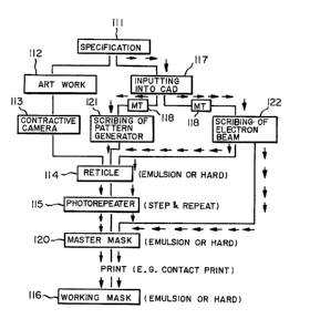
described below with reference to Figure 6.
In detail, a negative is produced using an art work
112 on the basis of a specification 111 having a number of items
on the optical recording medium described thereon and the thus
produced negative is contracted by a contractive camera 113 so
that an emulsion type or hard type reticle (intermediate mask)
114 is produced.
Then, the number of negatives is increased while the
., , ~
~ ! ' ' ` . .
~ 3 3 ~ 8 3 1
reticle (intermediate mask) 114 is contracted to an extent
of 1/10 or 1/5 of the original figure having sizes 10 to 5
times as large as the negative scribed on the reticle
(intermediate mask) 114 bY operating a photorepeater 115 so
that a master mask 120 is produced. A working mask 116 is
obtained by printing the master mask 120.
~ lternativelYl a magnetic tape 118 is produced by
inPuttin~ data thereinto with the aid of CAD as represented
by reference numeral 111. Then, while the magnetic tape 118
is used as an inputting medium, a reticle 114 is produced
by allowing the preformatting pattern to be automaticallY
exposed to a light beam on the high resolution plate
(HRP) using a pattern generator 121. Thereafter, a working
mask 116 is obtained by way of the steps as mentioned above.
Otherwise, while the magnetic tape 118 is used as an
inputting medium, a ~aster mask 115 is produced using an
electron beam exPosins apparatus 122 so that a working ~ask
116 is produced also by way of the steps as mentioned above.
DISCLOSURE OF THE INYENTION
Since the content of informations to be stored in a ROH
type optical recording medium dlffers from case to case,
there is a need of taking an adequate measure for
satisfactorily ~eeting the respective cases. When a number
of ROH tyPe optical recording mediums are produced, it is
. . .. ~
f; -- . . . .
,. . . . . . . . .
~. .. , . , , ~ ,
; -. . .. ..
~33~7
necessary to produce a master mask having individual data pit for
every ROM information data on the basis of specifications set for
the optical recording card. To this end, an expensive master mask
has been heretofore produced for every ROM information data,
resulting in the master mask for ROM type optical recording
mediums being produced at an expensive cost. Hitherto, when a
plurality of masks for ROM type optical recording mediums are
produced, an electron beam generator, a pattern generator or the
like apparatus are employed as exposing means. However, as a
quantity of information is increased, a time required for data
processing and a time required for a step of exposing are
elongated and moreover a long period of time is required also for
a step of inspecting a master mask, causing the master mask to be
produced at an expensive cost. It should be added that the
aforementioned method using the art work in that way is very
complicated in practical application.
The present invention has been made with the foregoing
background in mind and its object resides in providing a method of
producing a plurality of masks suitable for producing ROM type
optical recording mediums at an inexpensive cost.
To accomplish the above object, there is provided
according to the first aspect of the present invention a method of
producing a master mask for ROM type optical recording cards each
having the same preformatting pattern and data pit pattern as
writable type optical recording cards comprising steps of:
producing a mother mask having said preformatting pattern,
next, producing a master mask base board having a metal layer
B
,
.
.. ..
~; . .
~ 331~37
formed thereon on which said preformatting pattern is transcribed,
next, writing a data pit pattern by forming a number of pits
on said master mask base board by removing said metal layer in
correspondence to said data pit pattern by irradiating a laser
beam thereto in response to a control signal derived from said
preformatting pattern.
Further, according to a second aspect of the present
invention there is provided a method of inspecting a plurality of
mother masks, master masks or working masks for ROM type optical
recording cards each having the same preformatting pattern and
data pit pattern as writable type optical recording cards, wherein
said data pit pattern for said masks is read by a reading~writing
apparatus for inspecting the masks while the reading/writing
apparatus for said writable type optical recording cards is
controlled in response to a control signal derived from said
preformatting pattern, and decoded ROM information data are
compared with ROM information data prepared on the basis of
specifications set for said ROM type optical recording cards using
a computer.
Further, according to a third aspect of the present
invention there is provided a method of inspecting ROM type
optical recording cards each having the same preformatting pattern
and data pit pattern as writable type optical recording cards,
wherein said data pit pattern for said ROM type optical recording
cards is read by a reading/writing apparatus for inspecting the
ROM type optical recording cards while the writing/reading
apparatus for said writable type optical recording cards is
,
:''.': . .-~ :'
~33~837
controlled in response to a control signal derived from said
preformatting pattern, and decoded ROM information data are
compared with ROM information data prepared on the basis of
specifications set for said ROM type optical recording cards using
a computer.
Other objects, features and advantages of the present
invention will become more apparent from a reading of the
following description which has been made with reference to the
accompanying drawings
BEST MODE FOR CARRYING OUT THE IN~ENTION
Now, the present invention will be described in a
greater detail hereinafter with reference to the accompanying
drawings which illustrate preferred embodiments
r ~
:~ : .: , - : .
~ . . - .
330837
thereof.
The working mask which has been produced bY
transcribing a master mask in accordance with a contact
printing process or the like method is employed as a mask
which is emPIoyable for the purpose of Producing a number of
ROM tYpe optical recording cards in a mass production
system.
Firstly, the present invention will be described below
with reference to Fig. 1 which illustrates a series of steps
of producing a number of ROM type optical recording cards
usin~ the master mask for the ROM type oPtical recording
cards.
(1) A hard mask having a preformatting patten for writable
tYpe optical recording cards is produced. The preformatting
pattern comPrises a control pit pattern of which control
pits are prepared in the form of guides, track nu~bers or
the like (step of producing a mother mask as shown in Fig.
1(a)).
(2) Next, the preformatting pattern which has been formed
: on the mother mask is transcribed to a master mask blank
(with a laYer having a high reflectivitY formed on a base
board such a glass plate or the like) in accordance with an
etchiny process or the like method so that a base board
usable for the master mask is produced (step of producing a
base board for the master mask as shown in Fig. 1(b)).
O~ .
~;~,..';; ...
"~
~.-,,-
~ ~. .. ~ ... .
~ 1 33~837
(3) Next, a data pit Pattern is scribed on the master maskbase board having the Preformatting Pattern transcribed
thereto bY radiating a laser light in such a manner that a
writing/reading apparatus for writable type optical
recordin~ cards is controlled while performing a tracking
operation and a focussin~ operation in response to a control
signal derived from the Preformattins pattern and ROM
information data are encoded utilizlng a software for the
writable type optical recording cards (step of scribing ROM
infor~ation data as shown in Fig. 1(c)).
(4) Next, a ~aster mask is produced using the data bit
pattern while the master ~ask base board is processed in the
form of a pattern bY deYeloping, etching or the like process
(step of producing a ~aster mask as shown in Fig. l(d)).
(5) Next, a working ~ask is produced by transcribing the
prefor~atting Pattern and the data pit pattern from the
~aster ~ask (steP of producing the working ~ask as shown in
Fig. 1(e)).
(6) Next, ROM tyPe optical recording cards are produced
usin~ the working ~ask (step of producing ROM tyPe optical
recording cards as shown in Fig. l~f)).
As required, a step of inspecting the prefor~attins
pattern and the data pit pattern (as shown in Fig. 1(g) to
Fig. 1tl) is added to each of the foregoing steps so that a
quality controllin~ operation is performed during the
1~
~ . ~
:' ' '
. ' ' ' ' ' ~ ' ' ~ ~
~ , , .
3~0~37
respective steps.
The steps of inspecting (as shown Fig. 1(g) to Fig.
1(1)) are performed in such a manner that the
writing/reading apparatus for writable type optical
recording cards is controiled to read the data Pit pattern
while performing a tracking operation and a focussing
operation in response to a control signal derived from the
preformattin~ pattern and decoded data are comPared with ROM
information data prior to encodin~ with the use of a
computor for the Purpose of inspection.
Secondly, the present invention will be described below
with reference to Fig. 2 which illustrates a series of steps
of producing a ~other ~ask.
(1) First, a hard mask blank 9 is PrePared~ A chromium
~ask blank having a low reflectivity, e.g., ULCOAT PFl-5009
(S) L produced by Ulvac Coating Corporation, havins a light
shielding layer 12 of chromium or the like metallic material
for~ed on a base board 11 of glass or the like material is
used for the hard mask blank 9 (see Fig. 2(a)).
; As other type of hard mask ~aterial comprising glass
material ~representative of the base board 11), soda lime
blue (blue Plate glass), sode lime white ~white plate
glass), glass having a low expansion coefficient, synthetic
silica or the like material are emPloyable for the sa~e
purpose. As material other than glass, a material in the
~1
~ . .; -, - . . .
~s ~., ' ' ` . ,
133~837
form of a plate having an excellent surface smoothness ~ade
Of Polycarbonate~ polYmethylmethacrylate~
Polyethylenterephthalate~ epoxY or the like resin is
employable. It is preferable from the viewpoint of easy
usage that the hard mask board has a thickness in the range
of 0.05" to 0.0~".
Further, a ~aterial for the light shielding layer is
selected on the basis of a propertY of adhesiveness to the
base board 11, a property of light shielding and an aptitude
to etching. Typically, a single-layered structure of Cr, a
~ulti-layered structure of Cr/CrxOy or CrxOY/Cr/CrxOY, a
~etal layer of Al, Ni, Co, ~g, Au, Cu, Ti or the like
~etallic ~aterial, a chalcogenide based ~etal layer and an
alloy layer co~Prising the metal layer and the chalcogenide
based aetal layer as ~entioned above are employable for~ the
viewpoint of a proPerty of light shielding and a high
reflectivity. Particularly, a single-layered structure of
Cr and a ~ulti-laYered structure of Cr/CrxOy or
CrxCy/Cr/CrxCy are excellent in property of adhesiveness,
property of ligh~ shielding and altitude to etching.
(2) Next, a resist 13 is coated on the light shieldin~
laYer 12. TypicallY, the layer of resist 1~ having a
thickness of about ~.5 ~icron can be obtained by coating the
light shielding layer 12 with a positive type photoresist
AZ1350/SF Produced by Hoechet AG in accordance with a spin
. . . .
: ~ - . .
133~837
coating Process performed at ~,000 rpm for 60 seconds and
then prebaking the coated layer at a temPeratUre of 85
for 20 minutes (see Fig. 2(b))
In addition, an electron beam exPosing resist, e g ,
OEBR series positive type resist produced bY ~okyo Oka Kogyo
Co , Ltd can be used also In practice, a resist OEBR-1030
is coated at 3000 rpm for 60 seconds in accordance with the
spin coating process and the coated layer is prebaked at a
temperature of 170 ~ for 30 ~inutes ConsequentlY, the
resist la~er having a thickness of about 0 3 ~icron is
buiIt.
(3) Next, a light bea~ 14 (ultraviolet raY) is radiated so
as to allow a preformatting pattern 15 t~ be exPosed to the
light bea~ 14. As an exposing apparatus, Model NO. LZ-340
exposing apparatus Produced bY NSK Co., Ltd. can be used in
order that exposure is achieved under a condition of 180
~J/ QR. Inputtins of data concerning the prefor~atting
pattern 15 is effected by manual ~eans, a magnetic tape or
the like means each of which is used in association with CAD
(see Fig. 2(c)).
As other type of electron bea~ exposing apparatus, Hodel
NO. Havis III exposing apparatus produced by Perkingson-El~er
Corporation can be used. In this case, it ~oes without
saying that a resist for electron bea~ exPosure is used for
the purpose of exposing
l3
.,,
,.i, --
~33~837
(4) Next, the layer of resist 13 is developed. The
positive type photoresist AZ1350/SF produced by Hoechet AG
can be developed in such a manner that it is i~mersed for 30
seconds in a solution using a develoPer AZ-312MIF produced
by Hoechet A~ diluted with pure water by a volu~etric ratio
of 1 : 1 and thereafter it is sufficiently washed using pure
water (see Fig. 2~d)).
(5) Next, the light shielding laYer 12 is subjected to
etching. An etching solution having the following
composition is used.
a~moniu~ cerium nitrate 240 cc
perchloric acid (70 X) 60 cc
pure water 1000 cc
The light shieldin~ layer 12 is imDersed in the above
etching solution at a temperature of 20 ~ for 50 second so
that it is subjected to etching. After completion of the
etching oPeration~ it is sufficientlY washed using pure
water (see Fig. 2(e)).
As a co~ercially available etching solution,
Chro~e etchant K (trade na~e) produced by Nagase & Co., Ltd.
can be used too.
(6) Next, the resist 13 is removed. When the positive tyPe
photoresist A~ 1350/SF produced bY Hoechet AG is re~oved,
AZ thinner produced by the sa~e comPany can be used. The
hard ~ask blank 9 which has been subjected to etching is
~Y ~ .
-;~
~, . . .
Y
, .
. . . -. ,
,, . ,, :
133~837
i~mersed in the AZ thinner for about 5 minutes. After the
resist is dissolved therein, the ~other mask is rinsed in a
separate batch of AZ thinner and then it is dried (see Fig.
2(f~).
In a case where the resist OEBR-1030 produced by Tokyo
Oka KogYo Co., Ltd. is used, a removing liquid 502 Produced
by the same co~Pany is emPloyable as a co~mercially
available resist re~ovin~ solution. The above liquid is
heated up to a temperature of 100 ~ and the hard mask blank
9 which has been subjected to etching is then i~ersed in
the hot liquid for about 10 ninutes so that the resist 13 is
re~oved therefro~. After removal of the resist 13, the hard
Dask blank 9 is rinsed. A solution of mixture comprisins
acetone and ~ethanol by a volu~etric ratio of 1 : 1 can be
used as a rinsing liquid.
(73 The uother ~ask 2 including a preformatting pattern 15
is co~pleted b~ waY of the afore~entioned steps ~see Fig.
2(g)).
Thirdly, the present invention will be described below
with reference to Fig. 3 which illustrates a series of stePs
of producing a ~aster mask base board.
(1) First, a base board 21 is prepared (see Fig. 3(a)).
The hard ~ask base board which has been described abovc with
respect to the stePs of producing the ~other mask can be
used for the base board 21.
1~
~, .. .. .
~- ~
.
!;' ~'
~3~0837
(2) Next, a metal layer 16 is formed on th0 base board 21
(see Fig. 3(b)). The base board 21 is accommodated in a
spattering apparatus of which inner pressure is reduced to a
level of 1x10⁻⁵ Torr. Then, an argon gas is introduced into
the magnetron spattering apparatus so that an inner PreSsure
is ~aintained at a level of 1x10⁻³ Torr, With this
apparatus, a layer of chro~ium havin~ a thickness of about
700 angstro~s is deposited on the base board 21 at a
depositing rate of 10 angstroms per second. Consequently,
the resultant metal layer exhibits a reflectivity in the
range of about 50 to 60 X within the region of near-infrared
ray. Incidentally, the metal layer, the chalcogenide based
aetal layer and the alloy layer comprising the foregoing
~etal layers which have been used during the steps of
producin~ the ~other mask can be utilized for the metal
layer 16. The Present invention will be described further
below with respect to an e~bodi~ent wherein a layer of
chro~iu~ having a thickness of about 700 angstro~s is used
for the ~etal layer 16.
(3) Next, a resist 23 is coated on the ~etal layer 16 (see
Fig. 3(c)). The resist which has been used during the steps
of producing the ~other ~ask can be used for the resist 23.
~4~ Next, the ~other ~ask 2 is superposed on the base board
21 in such a oanner that the pattern surface of the for~er -co~es in close contact with the coated surface of the
~l33~37
latter. Then, the superposed structure is exposed to a
light beam emitted from a high pressure mercury lamp.
Exposure is achieved under an exposing condition of 4 mJ/ c~
(see Fig. 3(d)).
(5) Next, the resist 23 is developed (see fig. 3(e)). The
developing liquid which has been used during the steps of
producing the mother mask can be used as a developing
liquid.
(6) Next, the wetal layer 16 is subiected to etching (see
Fig. 3(f)). The step of etching permits the preformatting
pattern 15 to be transcribed to the master mask base board
20 from the mother mask 2. The etching liquid which has
been used durin~ the steps of producing the ~other ~ask can
be utilized as an etching liquid.
(7) Next, the laYer of resist 23 is removed fro~ the master
mask base board 20 wherebY production of the latter is
co~pleted (see Fig. 3(g)~. The removing liquid which has
been used during the steps of producing the mother ~ask can
be utilized as a remoYing liquid.
Fourthly, the present invention will be described
further below with reference to Fig. 4 which illustrates a
series of steps of producing a master mask.
(1) First, a ~aster mask base board 20 is prepared (see
Fi~. 4(a)). The ~aster ~ask base board 20 is such that the
preformatting pattern 15 is transcribed thereto by waY Of
Il
.,
.~ ,
~3~0837
the steps as shown in Fis. 3.
(2) Next, an optical recordin~ layer 31 comprisin~ dYestuff
and resin is formed on the master mask base board 20 (see
Fig. 4(b)). It is preferable that a co~poundin~ ratio of
dyest~ff to resin is set to a ratio of 1 of dyestuff to 1 of
resin to assure an excellent property of resistance against
an acid. With respect to the dyestuff, a material which is
excellent in a property of writing ROM information data
(representative of a ~aterial which is capable of
excellently absorbin~ a writing laser li~ht) is selected.
On the other hand, with respect to the resin serving as a
binder, a material which satisfactorily resists against the
etching liquid during the step of etching is selected. for
exa~ple, in a case where a se~iconductor laser light having
a wavelength of 880 nm is used as a writing laser light, a
dyestuff liquid havin~ the following composition is
enployed.
infrared raY absorbing dyestuff IR-82V
produced by NiPPon Kayaku Co., ltd. 1 part ;
nitrosellose H1J8 produced by Taihei
Che~icals Li~ited 8 parts
cyclohexanone 75 parts
1.2-dichloroethane 75 parts
The dyestuff liquid which has been prepared by dispersing
the above components therein in a ~ixed state is coated on ~ ~;
g
'. ''
J . ' ., ' ' ~ '.' ~ . : :
:,, ' . .- . "~, ' ~ :
~'
~3~0837
the metal layer 16 bY ~eans of a spinner in accordance with
a spin coating process performed at a rotational speed of
1,000 rpm for 60 seconds so that an optical recordin~ layer
31 having a thickness of about 2,000 angstroms is produced.
When it is assu~ed that the metal layer 16 (chromiu~ layer)
has an absolute reflec~ivity of 52 % relative to
near-infrared rays, reflectivities of the metal layer 16 and
a glass portion 33 as seen from the surface of the optical
recording layer 31 (surface representative of ~he dyestuff
layer) are represented by about 17 % and 5%, resPectivelY.
Consequently, when a semiconductor laser light havins a
wavelength of 830 n~ is used, a sufficient contrast can be
obtained. Since there is a possibility that a light
interference occurs with the optical recording laYer 31 and
the ~etal layer 16 under circu~stances, it is required that
a thickness of the optical recording layer 31 is properly
selected in dependence on the kind of resin, the kind of
dyestuff, the ratio of resin to dyestuff in co~position and
the ~aterial used for the ~etal layer 16.
(3) ~ext, controlling for a tracking operation, a focussing
operation and so forth is achieved on the basis of the
prefor~atting pattern 15 which has been formed on the master
nask base board 20 and ROM infor~ation data are encoded
using a writingtreading apparatus for writable type optical
recording cards so that the encoded infor~ation data are
~33~837
written in the form of a data pit pattern 34a (see Fig.
4(c)). Writing of the ROM information data is effected
while the master mask base board 20 is conveyed. In a case
where a semiconductor laser beam having a wavelength of 830
nm is collected on a spot having a width of 5 microns, the
optical recordin~ layer 31 can be re~oved in the form of a
number of spots by radiating thereto an energy having an
intensity of 8 ~W for 20 microseconds and the data pit
pattern 34a can be formed on the master mask base board 20.
The ROM infor~ation data to be ~ritten are such that theY
are expressed in the form of a manuscript prepared by a word
processor, a program or a photographic Manuscript. Then,
the ROH information data are scribed in accordance with the
for~at for the writable type oPtical recording cards, e.g.,
in such a manner that theY are introduced into a HS-DOS
file, each file is segmented bY every 256 bites, inserting
and arran~ing of data are performed so as to adapt to a ;~
format for the writable type oPtical recording cards,
editing of user data such as producing of a directorY or the
like is effected using a microcomputor, a tracking operation ~;
and a focussing operation are perfor~ed in accordance with
the preformatting pattern.
(4) Next, a data pit Pattern 34 is formed on the master ;~
mask base board 20 bY etching the data pit pattern 34a ~hich ~-
has been recorded bY writing the data concerning the ROH
~0
'',`'' '' , ~ " : . . '
~33~37
informations (see Fig. 4(d~). The etching liquid which has
been used during the steps of producîng the mother mask can
be utilized as an etching liquid.
(5) Next, the remaining optical recording layer 31 is
removed from the master mask base board 20 using a solvent
(see Fig. 4(e)). ~n acetone is used for the solvent. The
optical recording layer 31 can be re~oved from the master
~ask base board 20 by i~mersing it in the solvent for 10
seconds. Then, it is rinsed using another batch of acetone
and thereafter it is dried.
(6) Thus, production of the master mask 35 is completed
(see Fig. 4(f)).
(7) Incidentally, as required, the ~aster ~ask 35 is
inspected (see Fig.(g)).
Further, the present invention will be described
further below with reference to Fig. 5 which illustrates
another series of steps of producing a ~aster ~ask base
board and a master ~ask.
(1) First, a master ~ask base board 20a is produced (see
Fig. 5(a)~. In Practicel the master mask base board 20a is
produced in such a ~anner that the 0etal layer of ~etal
having a low melting point is used for the metal layer 16
during the step of producing the ~aster ~ask base board 20a
as sho~n in Fig. 3 and an etching liquid suitable for the
metal layer of ~etal having a low melting point is used for
~\
.. .
.,
~33~837
the foregoing purpose. A chalcogenide based metal layer and
an alloy layer comprising the mstal layer of Al, Ni, Co, ~g,
Au, Cu, Ti or the like and the shalcogenide based metal
layer can be used for the metal layer 46 of ~etal having a
low melting point. (It should be no~ed that an intermediate
layer ~ay be disposed between the base board 21 and the
~etal layer 46 of metal having a lower ~elting point in
order to assure that a property of adhesiveness to the base
board 21 and a sensitiveness during a period of writing
using a laser beam are i~proved.) Here, description will
be made below as to a case where a layer of Te having a
thickness of 5Q0 angstro~s is used for the metal laYer 46 of -~
~etal having a lower ~elting Point~ A layer of Te having a ~ ~1
thickness of 500 angstroms has light reflexibility of about :~
65% and light trans~issivity of 10% or less which is sufficient
light shielding capability for ~ask. A single iayer of Te
can be formed on the base board 21 by e~Ploying conventional
laYer forming ~eans in accordance with a spattering process ~-
or the like method. For examPle~ an etching liquid havins
the following composition can be used for the ~aster ~ask
base board 20a which has been for~ed using the ~etal layer
46 of metal having a lower melting point. ~;
nitric acid 1 part
hydrochloric acid 1 part -
phosphoric acid 8 parts
~, . ~, .: ',
~'': .' '''
~33~83~
pure water 9 parts
These components are ~ixed with each other by the
above-noted ratio and the master ~ask base board 20a is
im~ersed for about 30 seconds in the etching liquid which is
held at a te~perature of 20 ~ so that the master mask base
board 20a having the preformatting pattern 15 formed thereon
is obtained.
(2) Next, ROM information data are encoded by a
reading/writing apparatus for writable type optical
recordin~ cards while controlling for a trackin~ operation,
a focussing operation or the like is performed using the
preformatting Pattern 15 on the master mask base board 2Qa
and then writing of a data pit Pattern 34 is effected (see
Fig. 5(b)). ROM inforDation data can be written in such a
manner that a se~iconductor laser beam having a wavelength
of 830 n~ is collected on a spot having a width of 5 ~icrons
and an energy having an intensity of 12 mW for ~0 micron seconds
is radiated to the spot in the form of pulses so that the data pit
pattern 34 is for~ed directly on the ~aster mask base board 2Qa.
(3) Thus, production of the master mask 3~ is comPletsd
(see Fig. Stc)).
(4) Incidentally, as required, the ~aster mask 36 is
insPected with respect to its pattern using the
writing~reading apparatus for writable type optical
recording cards (see Fig. 5(d)).
'~ 3
~, ~
~,.",; . ~
. .
.
.:
~33~37
A working mask 60 (not shown) can be Produced using
fflaster masks ~5 and 36 by waY of the same steps as those of
producing the master mask base board. AS required, the
working mask 60 is insPected.
Next, description will be made below as to a method of
producing optical recording cards each including an optical
recordin~ medium which has been produced usin~ ~he working
~ask 60 of the present invention.
In Figs. I and 8, reference numeral 41 designates a ROH ~:
type optical recording card. The ROM type optical recordins
card 41 is so constructed that an optical recording portion
45 is interposed between two card base baords, i.e., between
a front card base board 42 and a rear card base board 43.
The front card base board 42 is made in the form of a plate
of transparent resin having an excellent flatness such as
polycarbonate, poly~ethyl~ethacrylate, ePoxy or the like
resin material. On the other hand, the rear card base board
43 is ~ade also in the form of a plate of resin such as ~-
polyvinyl chloride, polycarbonate, polyethyleneterephthalate ~
or the like resin material. ~ -
The working mask 6~ which has been produced in
accordance with the present invention is used to for~ the
optical recording portion 45.
Next, description will be made below as to a method of
producing ROH tYpe optical recording cards.
,- .. ,-. . - .. ~ . - -
~i
-
~3308~ ~
First, a method of producin~ a ROM type optical
recordin~ cards 41a bY producing an information Pattern on
the front card base board 42 using a metallic reflective
laYer (indicative of an aluminum layer 49a) is as shown in
Fig. 9.
I1) First, as shown in Fig. 9, a transparent front card base
board 42 of PolYcarbonate having a thickness of 0.40 mm is
prepared (see Fig. 9(a)).
(2) Next, acryl-silicon resin 1161 produced by Dainippon
Ink & Chemicals Li~ited is coated over the outer surface of
the front card base board 42 in accordance with a roll
coating process so that a dried layer having a thickness of
about 5 microns is obtained. Consequently, a hard coated
layer 47 is for~ed (see Fig. 9(b)).
(3) Next, acryl-silicon resin 1161 produced by the sa~e
com~any is coated over the inner surface of the front card
base board 42 in accordance with a roll coating Process so
that a dried layer having a thickness of about 5,000
angstro~s is obtained. Thus, an anchor layer 48 is for~ed
(see Fig. 9(c)).
(4) Next, an alu~inu~ layer 49a is formed over a region
corresponding to the optical recording portion 45 on the
front card base board 42 in a vacuuD deposition process
performed at a deposition rate of 20 angstro~s per second
under a degree of vacuum rePresented by 2x10⁻⁵ Torr so that
~5
;. . ,
,~ .
;; . .
-
133~8~7
the dePosited layer having a thickness of about l,OOO
angstroms is obtained (see Fig. 9(d)).
(5) Next, a photoresist Microposit (registered trademark)
S1400-11 produced by Shiplay Far East Ltd. is coated over
the aluminum layer 49a on the front card base board 42 by
operating a spinner at a rotational speed of 3,000 rpm for -~
30 seconds so that the drY coated layer having a thickness
of about 5,0D~ angstroms is obtained. Thereafter, the
coated laYer is Prebaked at a te~perature of 90 ~ for 15
minutes. Thus, a resist layer 51 is formed ~see Fi~. 9(e)).
(6) Next, a working mask 60 having a required data pit
pattern (representatiYe of ROM information data ) formed
thereon is caused to come in close contact with the resist
layer 51 on the front card base board 42. Then, the
asse~bled structure is exPosed to light beam under a
condition of 4 ~J/a2 using a ~ercury lamp so that an
optical recording Pattern !ayer 51b is for~ed (see Fig. ~ :
9~f)).
(7) Next, the resist layer 51 on the front card base board
42 is develoPed for 30 seconds using a developing liquid
which is prepared by diluting a developing liquid MF-312
produced by Shipley Far East Ltd. with pure water at a ratio
of one Part of the for~er to one part of the latter.
Thereafter, it is sufficiently washed with pure water and
then it is dried ~see Fig. 9(g)).
~D
P
~,
" . . ~ .
~!3~837
(8) Next, an etching solution having the following
composition is prePared in a mixed/stirred state.
(volumetric Part)
phosphoric acid 1B parts
acetic acid 2 parts
nitric acid 1 part
pure water 1 part
The aluminum laYer 49a on the front card base board 42 is
im~ered in the foregoing etching solution at a temperature
of 35 ~ for 50 seconds using an oPtical recording pattern
laYer 51b as a mask so that it is subjected to etching.
After an aluminum pattern 4gb is formed, it is washed with
pure ~ater and then it is dried (see Fig. ~(h)).
(9) Next, to assure that a propertY of removal of the
photoresist on the front card base board 42 is imProvedl the
latter is exposed to a light beam again under a condition of
100 mJ/ o~ and it is immersed for 1 to 2 seconds in a
solution which is prepared by diluting a re~oving liquid
( HAKURIEKI 10 -trade name-) produced by Tokyo Oka Kogyo
Co., Ltd. ~ith pure water at a ratio of one part of the former
to 3 parts of the latter so that the oPtical recording pattern layer
51b is removed fro~ the front card base board 42. ImmediatelY
after removal of the optical recording pattern laYer 51b, the
front card base board 42 is sufficiently washed with Pure water
and then it is dried (see Fig. 9~i)).
~1
'a ~
.', ......... . .
~ .
- 133~37
(10) Next, a laYer of adhesive 52 comPrisin~ an urethane
based thermoplastic adhesive is previously coated over the
inner surface of the rear card base board 4~ in the form of
a sheet of polyvinyl chloride having a thickness of 0.35 mm
in accordance with a roll coating process until the
resultant dried layer has a thickness of 5 microns. Then,
the inner surface of the front card base board 42 is brought
in close contact with the inner surface of the rear card
base board 43 in a superposed state. Thereafter, they are
adhered to each other by subjecting them to hot pressing at ~
a te~perature of 90 ~ for 10 minutes under the effect of ~ -
pressure of 15 Kg/~ (see Fig. 9(i)).
(11) Next, the resultant structure is cut to sizes
corresponding to the configuration of an ordinary card (see
Fig. 9(k)).
(12) Thusl production of the optical recording card 41a is
co~pleted (see Fig. 9(1)).
INDUSTRIAL APPLICABILITY
The present invention has Provided a method of
producin~ a plurality of ~asks for ROM type optical
recording cards wherein a preformatting pattern (representative
of a logical structure for reading and writing data) in the
form of a control pit, a guide or the like for ROM type
optical recording cards and writable tYpe optical recording
~Lg
F-` ~ ' ~ .` . .. .
r?~
~"1 '` , . ' : . :
133~837
cards is identical to a data pit. According to the present
invention, a writing/reading apparatus for writable type
optical recording cards can be utilized as an inspecting
instrument for inspecting a mother mask, a master ~ask and a
w~rking ~ask for ROM type optical recording cards as well as
an inspecting instrument for inspectins the ROM type optical
recording cards with the result that an inspecting operation
during a step of producing these masks as well as an
inspecting operation during a step of Producing the cards
can easily be performed without any necessity for
exclusively designed inspecting instrument. Other
advantageous effects of the present invention are that a
syste~ (representative of a data processing system
co~prising a computor, outer memory units and so forth~
e0ployable for a writing/reading aPParatus for writable type
optical recording cards can be utilized as a scriber for ROM
information data and the sYstem e~PIoYable for the
writing/reading apparatus for writable type optical
recording cards can be utilized as a syste~ employable for a
reading aPparatus for ROM tYpe oPtical recording cards.
Owing to the aforementioned advantageous effects of the
present invention, a cost required for producing a master
~ask can be reduced remarkable and steps of producing masks
from the step of producing a mother ~ask to the steP Of
~roducing a workin~ mask can be simplified. In addition, it
r . . .
. .
': ~'''' , ~ .
;
" - ~ . :
~l 7
~L330~37
becomes possible to quickly meet the requirement for
producing many kinds of ROM type optical recording cards in
small production lot. Further, a cost required for
producing the ROM tYpe optical recording cards can be
reduced substantiallY.
In this ~anner, according to the method of producin~ a
plurality of masks for ROM type optical recording cards in
accordance with the present invention, since a preformatting
pattern (representative of a logical structure for reading and
writin~ data) for ROM type optical recordin~ cards and
writable type oPtical recording cards in the form of a
control pit, a guide or the like is used in common with a
data pit, ROM type optical recording cards produced using
the ~asks which have been produced in accordance with the
method of producing a plurality of masks for ROM type
optical recording cards per~it ROM information data to be
processed using a system for a reading/writing apparatus
e~ployable for writable type optical recording cards. Thus,
~asks for ROH tyPe optical recording cards can simply be
produced at an inexPensive cost. Further, according to the
present invention, since a Preformatting pit and a data pit
are not scribed on a hard ~ask blank in response to everY
ROM infor~ation data on the basis of specifications set for -~
these cards but ROM information data are scribed using a
system for a reading/writing apparatus e~ployable for
.
~,..... . .
, ~ ,
.. ...
. .
writable type oPtical recording cards on the assumption that
a ~other mask including a preformatting pattern (representative
of a logical structure for reading and writing data) for
writable type optical recording cards in the form of a
control pit, a guide or the like is produced and a master
~ask adapted to scribe ROM information data on the basis of
the mother mask is prepared for every specification set for
the cards, steps of producing a plurality of Dasks from the
step of producing a ~other mask of the step of producing a
master mask can quickly be performed at an inexpensive cost.
.
. - -: .
.
~, .