Note: Descriptions are shown in the official language in which they were submitted.
133~279
~ MAGNESIUM TITANATE CERAklIC
AND DUAL DIELECTRIC SUBSTRATE USING SAME
This invention relates to a multilayer ceramic
substrate or body having two adjacent layers of different
composition and dielectric properties, such as disparate
dielectric constants.
Such bodies are typically used as æubstrates that
include buried conductors and buried capacitors. Some such
bodies employ conductive vias for making electrical
interconnection between layers of conductors. It is also
known to metallize portions of an outer æurface of such
bodie~ and to mount discrete electrical components thereto,
e.g. semiconductor integrated circuits, and/or forming on
the body and in it film components such as resistors. It is
desirable to form such buried circuits and surface
components in and on a low dielectric constant (K) material
so as to minimize interwiring capacitance and consequent
,"crosæ talk". On the other hand, it is often highly
desirable to form buried capacitors within a high K body so
as to minimize the physical size and cost of the capacitor.
~e
7~i
j,, ' . ' A, , ' .. ,, ., . . , .. , ,, .. . , ~ i ~
-^ ` 13 312 ~ 9
The above-noted low K materials when combined in
the green state with a layer or layers of barium titanate
and sintered to a dense mature compound body, exhibit at
each interface wi~h the barium titanate, a band of an
integrated material wherein some of the elements of each of
the two start materials have co-reacted. This interface
band generally exhibits a gradient of dielectric properties,
e.~. K, DF, and TC, that are quite different than tha~ of
either start material, i.e. either of the low K material or
the high K barium titanate layer.
This interface band canno~ be used as a capacitor
dielectric in practice, because of its varying and uncertain
dielectric properties. The thickness of this interface band
of co-reacted material in compound prior art bodies has been
typically 0.025 to 0.065 mm (1.0 to 2.6 mils). It is good
practice to relegate even wider bands of material at such
interfaces to non-use and thereby safely avoid unexpected
and degraded performance of capacitors formed therein.
Also, the compound ceramic bodies of the prior art
that combined a high K barium titanate layer with a low K
layer have a strong tendency to develop catastrophic cracks,
due to the large differences in the thermal coefficients of -~
expansion of these two dissimilar materials. This severely
limits the overall compound-body size that can be reliably
manufactured.
Other prior art devices have a high K layer
sandwiched between two layers of a low K ceramic
composition, in which the outer layers are made as thick or
thicker than the high K layer to ameliorate the tendency of
these compound bodies for cracking. Such a limitation on
sandwiched ceramic bodies more often leads to thicker and
larger packages than desirable and than would otherwise be
necessary.
`` ~33127~
-- 3 --
A feature of the present invention is the
provision of a low K ceramic material that may be combined
in a composite body with and reliably co-sintered with a
barium titanate. Ano her feature is that said low K ceramic
material be chemically and physically compatible at
co-sintering with barium titana~e. Ano~her feature is to
ameliorate the above-noted shortcomings of the prior art.
Another feature is the formiation of a multilayer compound
ceramic body having an inner layer of barium titanate
sandwiched between two layers of ceramic material having a
K at leas~ 100 times less than the K of the barium titanate.
In accordance with this invention a low K ceramic
is a magnesium barium zinc titanate, the molar quantities of
barium and of zinc each being within 40 to 60~ the molar
amount of titanium. This low K material has a K less than
two orders of magnitude relative to the K of substantially
all ceramics comprised of more than 85 wt% BaTiO3. Further-
more, the low K ceramic has a commensurate coefficient of
expanslon, e.g. the shrinkage following sintering is within
about 10% that of such a barium titanate. In a compound
substrate this low K magnesium barium zinc titanate is also
chemically compatible with such high K barium titanates; a
narrow reaction zone and a strong bond are formed between
them.
In a further aspect of this invention, a substrate
has a layer of a barium titanate bonded adjacent one layer,
or preferably sandwlched between two layers, of the
above-mentioned magnesium barium zinc titanate; all having
been co-sintered. This invention provides a compound
ceramic sandwich wherein each layer in the sandwich is of
homogeneous ceramic composition in directions parallel to
the interface between layers.
~3~279
-- 4 --
In a drawing which illustrates embodiments of the
invention,
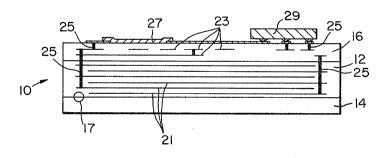
Figure 1 is a side sectional view of a multi-
layer compound ceramic substrate wi~h buried electrical
components formed within, and with electrical components
formed on and mounted to an outer surface o~ the substrate,
Figure 2 shows a magnified detail of portion 17 of
the substrate of Figure 1, and
Figure 3 is a side sectional view of another
multi-~ayer compound ceramic substrate.
A series of compound bodies were made and tested
to determine their suitability as multilayer compound-
ceramic substrates.
Example A
A number of substra~es 10, as illustrated in
Figure 1, were made having a high K layer 12 sandwiched
between two low K layers 14 and 16. Such substrates were
made by first preparing a ceramic slurry having a liquid
organic vehicle including a binder and a fine low K
ceramic powder of a magnesium zinc titanate. Subsequently
a green layer was formed by a standard method of
repetitively depositing and drying a stack of films of the
ceramic slurry to form a first green ceramic layer, to
: become layer 14. Such a standard method is further
described by Maher in US 4,266,265 issued May 5, 1981.
~331~
-- 5 -- .
Then, another ceramic slurry comprised of the
liquid organic vehicle and a high K ceramic powder was
repetitively deposited and dried with intervening films of
electroding ink to similarly form a second green layer, to
become lay~r 12, on the first green layer 14. Another low K
layer, to become layer 16, was formed again by tha same
method on the green high K layer 12. After heating to about
400C to drive off the binder, that stack or compound body
o~ green ceramic layers 14, 12, 16 was then fired at 1100C
for 2i~ hours to drive off the organic materlals ~nd to
co-sinter the green layers to form mature high K layer 12
and low K layers 14 and 16 that are by that sintering step
co-reacted and bonded together. The mature ceramic layer 12
has the composition ~1 and the ma~ure outer ceramic layers
14 and 16 have the composition #3 o the compositions
defined in Table I by molar quantities in subscripts and by
weight in parentheses.
Table I
COMPOSITIONS
1. (loo)BaTio3(l.o)Bi2o3(l~o)pbo
(l.O)ZnO(1.7)Nb2O5(0.7)B2O3
2. (97)BaTiO3(1.0)Nb2O5(2)5CdO 2SiO2
) g0.67Zn0.33TiO3(2)CdZn2B2O6
4 (98)Mgo 5Ba0 25Zn0 2sTiO3(2)CdZn2B2O6
5. (98)Mgo 65Ba0 10Zn0 2sTiO3(2)Cdzn2 2 6
6. (98)Mgo 35Bao 40Zn0 2sTi3(2)cdzn2B26
~- :L3~
-- 6 --
Sintering at 1100C was made possible by the
inclusion of composition ~2 silica-based sintering flux.
The barium, titanium, niobium and other elements were
included in the start powder of composition ~1 as the oxides
BaO, TiO2 and Nb205. Likewise the start powder of
composition ~3 was comprised of oxides (or oxide equivalents
such as carbonates and oxylates) of magnesium, zinc, or
titanium. The making of compound substrates by this method
leads to a thick and pronounced reaction band formed at the
interface between adjacent layers of the high K and low K
materials.
A second making of substrates by this method used
a prereacted magnesium ~inC titanate, i.e. Mgo 67zno 33TiO3
which was calcined at 1150C before introduction ~o the
start materials.
These later-made substrates were sectioned and a
portion 17 of the interface region between the low K layer
14 and the high K layer 12 was magnified by electron
microscope (lOOOX) and is illustrated in Figure 2. There, a
still pronounced and well-defined interface-band 18 was
seen, but band 18 is of a reduced thickness 19 of about 1.5
mils (0.06 mm). It is thus preferable to precalcine the
barium titana~e of composition ~1.
Analysis of the average composition of this
interface band 18 was determined by SEM to be
Mgo 5Bao 25ZnO 25TiO3. However, interface band 18 of the
co-reacted material is not homogenous and is believed to
have a wide range of compositions and dielectric properties
in a direction from the low K to the high K layers.
~3~ 7~
-- 7 --
Figure 1 also shows buried metal-film electrodes
21 forming plates of a buried capacitor formed in the high K
material of layer 12. There are also metal film conductors
23 buried in the low K material of layer 16 which are
interconnected by conductive vias 25. On the surface of
low K layer 16 there is formed a film resis~or 27 and there
is attached an integrated circuit package 29.
High K materials are advantageous in those areas
in which capacitors are buried, and low K material is
advantageous in other areas of a wiring board in which
buried low-cross-talk wiring layers are desired.
Conventional methods may be used to provide these buried
electrodes and conductors, e.g. printing patterns of
electroding ink between successive depositlons of ceramic
slurry and cofiring with the ceramic. Such conventional
methods are described by Maher in US 4,633,366 issued
December 30, 1986. Neither the experimental subs~rates of
Example 1 nor any of the following Examples, except where
noted, included these additional features.
Example B ~combining ~1 wi~h #4)
Another group of substrates were made by the same
steps as were used for making the later-made Example A
substrates, except that the low K composition #4
(corresponding to the average composi~ion found in
interface reaction bands 18) was substituted for the low K
composition ~3 in layers 14 and 16.
At the interfaces between high K and low K layers,
e.g. 12 and 14 respectively, ~here is a mild and barely
perceptible reaction band at 1000X magnification and it is
about half the width of the prominent reaction band 18 in
the Example A substrates. For practical purposes, the mild
reaction band has been eliminated, since very little
diffu ion and reaction of elements from either layer has
taken place in the other.
~3~q ~7~
Example C (combining ~2 with ~4)
Yet another group of substrates of the kind
illustrated in Figure 1 were made. The high K start
material was a precalcined barium titanate doped simply with
niobium to which a borate flux was added (composition #2 in
Table I). The low K start material was the precalcined
magnesium barium titanate with a silicate fl~r added
~composition #4). The amount of binder in ~he start slurry
from which the outer low K layers are to be formed was
empirically adjusted so that the amount of shrinkage of the
outer layers from the green state to the sintered state was
about equal that of the cen~er high K layer~
The faint reaction band in these substrates seen
at 1000X magnification was essentially of the same character
and extent as that in substrates of Example B. There is
found the usual trade-off between K and temperature
coefficient of capacitance (TCC) referring to Table II, but
it appears tha~ all high K ~K 1500) barium titanates
(defined herein as ceramics having more than about 85 wt~
BaTiO3) will co-sinter similarly with low K magnesium barium
zinc ti~anates, e.g. those wherein the barium and zinc are
each present within about 40 to 60 mole % of the magnesium.
Table II
.
. PROPERTIES OF COMPOSITIONS
.
~ K TC
_ _ . _ _
1. 2600 X7R
2. 4300 X7S
3. 20 COG
. 4. 23.6 COG
5. 21.3 COG
6. 64 COG
. . I .
~,, ,. , .,, . ~,. . . . .
--::: :'-.:
- ~33~
_ 9 _
Example D (TCE measurements)
A siet of experimental substra~es were made as
follows:
D-l composed entirely of ceramic composition #l;
D-2 composed entirely of ceramic composition #2;
D-3 composed of one low K layer of composition #4;
D-4 composed of a high K layer 6 mils (0.15m~) thick
of composition #l sandwiched as in Figure 1
between two layers 15 mils (0.38mm) thick of low K
ceramic composition ~3; and
D-5 composed of a high K layer 6 mils thick of
compostion #2 sandwi~hed as in Figure 1 between
two layers 15 mils thick of low K ceramic
composition #3.
The length of each substrate is 340 mils (8.5mm) while the
thickness of each substrate is be~ween 34 and 38 mils. By
monitoring the length of each substrate as it cooled from
the peak sintering temperature of 1100C to 25C, it was
seen that the substrates D~3, D-4 and D-5 shrank essentially
the same amount, viz. from 12 to 12.7Z; whereas substrates
D-l and D-2 shrank 14X. From these data it seems certain
that in the sandwiched constructions, the center layer 12 of
high K material is under tension zt room temperature (25C).
Since ceramic material~ are much stronger in
compression than in tension, one would conclude from these
data that it would be preferable to provide two low K layers
14 and 16 having a total thickness much greater than the
high K layer 12.
However, the sintered substrates were then
subjected to testing by slowly increasing the temperature
,from 15C to 475C while measuring their change in length.
The TCE for each substrate was calculated and is presented
in Table III.
".
. ~ : :- . . .
. - . .
- 10 - 1`~3~27.~
Table III
TCE
Substrate 10~6mm/mm/C
D-l 10.7
D-2 11.4
D-3 9.9
D-4 10.2
D-5 10.2
The TCE of these two compound substrates D-4 and D-5 also
tracks very closely the characteristic T OE of the low K
layers D-l and D-2~ The high K layer in each case being in
a state of tension at room temperature is apparently elastic
enough to follow ~ery nearly the dimension of the outer
layers. In a series of experiments, thickness of the outer
15 layers was varied from being equal to the thickness of the ``
inner layer to being three times that thickness. The
incidence of cracks in the inner layer became less as the
outer layer thickess became less.
Th~s it is preferred to keep the low K outer
layers relatively thin; namely, less than half the thickness
of the inner layer.
Example E (combining #2 and ~5)
The experiment of Example C was repeated except
the low K material composition ~4 was altered whereby a ~ -
lower molar ratio of zinc to magnesium (0.39) was effected
to produce the composition ~5 (Table II). These ra~ios in
composition #4 were both 0.5. These parts crack~d at the
middle of the high K layer because of greater stresæes in
the composite substrate during cooling from the 1100C
firing.
Example F (combining ~1 and $6)
The experiment of Example C was repeated again,
e~cept this time the low K material composition ~4 was
~; altered whereby a higher ratio of barium and zinc to
; 35 magnesium was effected. There was no splitting of these
units as they cooled, but K was ralsed substantially to 64
(Table II) and the dielectric constant ratio of the high K
layer to that of the low K layers drops well below the
desired ratio of at least 100.
: : .:
33~ 2~9
Example G
A number of experimental substrates were made
composed o a 16 mils (0.4 mm) thick high K layer o
composition #l sandwiched between two layers of 5 mils
(0.13 mm) thick low K ceramic composition #4 of this
invention. The overall thickness of each sintered compound
substrate of Example G is abou~ 27 mils (0.69 mm). The
length and width are 120 mils (3.0 mm) and 60 mi1s (1.5 mm).
The strength of these compound substra~es was
compared with a number of substrates having the same overall
dimensions but being composed only of composition #l in one
series and only of composition #2 in another. These data
are shown in Table IV.
Table IV
SUBSTRATE COMPOSITIONS
$1 ~2 Example G
Average Thickness (mils) 28.4 23.5 26.9
Average Fracture (lbs.) 3 5.3 11.8
Number of Substrates 8 8 16
Substrates of the same sandwich composition and
structure, ~xample G, except having length and width
dimensions of 1 inch by 1 inch (26 D~ X 25 mm) were made
with no cracks.
The sintering flux 5CdO~2SiO2 is not critical and ;
may alternately be Cd3SiO5, Cd2SiO4, CdSiO3 or mixtures -~
thereof, or any of many sintering fluxes that reduce the
sintering temperature of the barium titanate composition,
e.g. composition $2 of Table I. Likewise, the sintering
flux in the low K material of this invention may be
6 9 9 dZnB2O5, Mg3B2O6 or combinations of these
borates.
~3~2~
- 12 -
A compound ceramic substrate ~0 is illustrated in
Figure 3. Two m~ltilithic ceramic capacitors were formed
in two bsrium titanate layers 22 and 24. Each capacitor
layer 22 and 24 was sandwiched between a pair of layers of
composition ~4 o this invention; respecti~ely, pairs 26 and
28, and pairs 28 ar.d 30. In thls structure the capacitors
in layers 22 and 24 are dielectrically i~olated from each
other by low K layer 28 and from any wiring or components
that may be formed in and on the outer low K layers.
Another ceramic sandwich structure, employing a
fine and nearly monodisperse ceramic as an inner layer while
the pair of outer layers have a broad range of ceramic grain
sizes, is di~closed by Maher in Canadian patent application nulbber
605,975 ~iled on July 18, 1989 entitled "MONOLITHIC COMæOUND-CER~MIC
CAPACITOR".
, ;. ,~ :
.
::. :.:~ :; - , -
, , -