Note: Descriptions are shown in the official language in which they were submitted.
t 331 783
Field o the Invention
This invention relates to a surge absorber and more
specifically a device composed o a microgap type surye
absorbing element and a varistor electrically connected in
series to each other.
Prior Art
The ZnO varistor is characterized by a quite remarkable
nonlinearity of the characteristic voltage-current (V-I)
curve. Thus, assuming an equation I = kV~ for the above
characteristic curve, the voltage nonlinearity factor ~ of
this type of varistor is mostly in a range from 25 to 50,
though sometimes even higher than 5~. This favorable
nonlinearity characteristic has hitherto been used for surge
absorption. As a voltage is applied, ~owever, the ZnO
varistor as characterized above leaks current, so use
thereof for long time with a voltage continuously applied
thereto gradually undergoes deterioration in the
voltage-aurrent characteristic property causing such a
danger that the varistor may break down and short-circuit
resulting in a thermal runaway.
In order that the above ZnO varistor might stay ready
to work with a high surge response characteristic of its own
while suppressing the aforementioned leak current to a
minimum level for prevention of the deterioration thereof
and avoidance of the accompanying danger as mentioned above,
1 3 3 1 7 P,3 ~
there was disclosed a surge absorber composed of a
Zno varistor and a microgap type surge absorbing
element electrically connected in series ~Japanese
Unexamined Patent Publication No. 58-95933). The
above surge absorber however uses a ZnO varistor
which is characterized by a large voltage non-
linearity factor a and thus selected among those
products having a varistor voltage higher than the
lo line voltage.
As mentioned above, the surge absorber of
prior art uses a ZnO varistor whose varistor voltage
is higher than the line voltage, so the above surge
absorber is characterized by high firing potential
and surge response voltage, nece6sarily resulting in
a slow surge response. Accordingly, the above surge
absorber has a problem of small discharge capacity
that means a surge absorption capacity insufficient for
protection of devices.
SummarY of the Invention
An object of the invention is to provide
a surge absorber characterized by a superior surge
absorbing property.
The surge absorber to which the invention
relates is composed of a microgap type surge absorbing
element and varistor electrically connected in series, the
above varistor being characterized both by a varistor
voltage lower than the line voltage and a voltage
nonlinearity factor satisfying an inequality 1 < a 20.
Preferably, the nonlinearity factor a iæ between S and 10,
and the varistor is of a type selected from the group of
f,
~t
^ 1 33 1 7~33 ~:~
Tio2~ SrTiO3, SiC or SnO2.
Brief description of the drawin~s
Figure 1 is an equivalent circuit of a surge
absorber embodying the invention. Figure 2 i6 charac-
teristic voltage-current curves given to describe the
working mechanism of the surge absorber of this
ld invention. And Figure 3 and 4 are vertical the
vertical cross-section of surge absorbers adopted in
individual Examples. In these drawings, there
appear~
Microgap type surge absorbing elements 2, 4,
9;
Varistors 3, 4, 10; and
Characteristic voltage-current curves a, a', b,
b'.
Detailed DescriDtion of the Preferred Embodiment
Figure 1 is an equivalent circuit of a surge
abeorber l composed of a microgap type surge absorbing
element 2 and varistor 3 electrically connected in series.
Referring to Figure 2 wherein several possible
characteristic V-I curves of varistor 3 are shown, the
varistor's voltage nonlinearity factor a as expressed a =
1/log10(V10~/V1~) gives a measure of the slope of the V-I
curve between 1 mA and 10 m~. The V-I curve "a" of a
varistor with a smaller a has a steeper slope than the V-I
curve "b" of a larger a.
The varistor 3 must be built in the aforementioned
surge absorber 1 in such a circuit design that any damage to
,
.;
-: .
13317P~3
-
the microgap type surge absorbing element may be avoided.
Naturally, this requires selection of a varistor that has a
varistor voltage (vl~) high enough to suppress any follow
current. A requirement for such varistor is that the line
current I~ as determined by a point where the line voltage v~
crosses the V-I curve "b"' must be smaller than the arc
maintaining current IA~ namely, an inequality I~ must be
satisfied.
The ZnO varistor that has been used in the
prior art surge absorber is characterized by a
characteristic V-I curve "b". As long as the
inequality I~ ~ IA is satisfied, however, no follow
current flows, so it is possible to use a ZnO
varistor that is characterized by a characteristic
V-I curve "b"' with the varistor voltage VO thereof lowered
down to VO'. Further, referring to a varistor characterized
by a characteristic V-I curve "a" having a steeper slope
between 1 mA and lo mA, namely, a smaller value for the
afore-mentioned parameter a than the curve "b"', the current
IL~ as determined by a point where the line voltage VL
crosses the characteristic V-I curve "a" is smaller than IL~
namely IL~ ' IL' for the voltage change between V1~ and V10
is larger with the curve "a" then with curve "b' n .
Accordingly, it is possible to move the characteristic
V-I curve "a" to the right until it overlaps the
curve "a"' with the varistor voltage VO~ of the
curve "a" lowered down to VO".
Accordingly, varistor 3 of Fig. 1 has varistor
voltage lower than the line voltage and a voltage
nonlinearity factor a satisfying an ineguality 1 a 20 in
the above surge absorber 1. A surge absorber was thus made 7
that had lower firing potential and surge response voltage
~i
.,
~ `' ' . :' ' ' ` ' '. .
t-~3 1 7~3
,
with a faster surge response and was further characterized
by lower after-surge response residual voltage, as compared
to the aforementioned surge absorber of prior art. Namely,
S a surge absorber characterized by a superior surge absorbing
property was discovered.
A microgap type surge absorbing element as
disclosed by the present inventors in the aforementioned
Japanese Unexamined Patent Publication 54-95933 and also
lo Japanese Unexamined Patent Publication 55-128283 may
preferably be used as such herein. The above surge
absorbing element is a solid circuit element composed of a
conductive film formed on the ~urface of an insulator body
with microgaps lo to loo ~m in width dividing the conductive
film into several parts wherein an electrode to which a lead
is connected is secured to both end parts of the divided
conductive film, the area of the conductive film between
these electrodes being enclosed by an insulating material
with an inert gas, such as argon, neon, or the like, sealed
in. The only requirement for the above element is a firing
potential that is higher than the maximum working voltage of
a circuit in which the element is built in. The discharge
start voltage is properly set for varistor selection
according to the type, characteristics, etc. of the circuit
to be protected.
Any varistor may be used herein as long as the
varistor voltage thereof is lower than the line voltage and
the voltage nonlinearity factor a thereof satisfies the
inequality 1 a 20, though a varistor is preferably of
TiO2, SrTiO3, SiC, or SnO2 type and the factor a thereof is
preferably between 5 and 10.
The microgap type surge absorbing element and
varistor may be connected by any mean6 as long as a positive
~ ~, .. , . ,, , . ,, , , .. 1 .~ ............ . . . . . .. . . . . . .. .
~ 331 783
electrical conneetion i6 established therebetween, though
calking, soldering, wiring on a circuit board, etc. may
conveniently be used.
To stabilize the shape of the surge absorber of
this invention, the entire assembly thereof is preferably
covered with an insulator casing, coating material, heat-
shrinkable tube, or like with or without being charged with
a filling material.
The surge absorber of this invention can be built
in a large variety of electrical devices, instruments and
equipment, being favorably used particularly in those having
power lines, disposed between these lines or one of these
lines and ground.
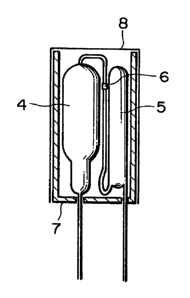
EXAMPLE 1
Figure 3 is a vertical cross-section of a surge
absorber composed of a surge absorbing element 4 and
varistor 5 electrically connected in series by calking 6,
both accommodated inside of a cylindrical insulating cup 7
covered with a heat shrinkable tube 8. Surge voltages were
applied to the surge absorber as constructed above for an
experiment as follows.
An SrTiO3 varistor with a = 10 and varistor voltage
= 20 V was used with a surge waveform of (1.2 x 40) ~sec -
5 kV.
For control, the same experiment was repeated
using a ZnO varistor with a = 60 and varistor voltage = 220
V ~
_
~.~
1 33 1 7~3
instead of the above varistor.
Tables 1 and 2 are the experimental conditions and
results, re~pectively.
Table 1
Line , firlng IPtential Vari~tor's
voltage of surge Nonlinearity Varistor
absorbing element factor ~ voltage
Ex. 1 120 VAC 300 V 10 20
Cont. 1120 VAC 300 V 60 220
Table 2
flrlbg Surg~ re~pon~e After-surge-
potentlal voltage residual voltage
. .
Ex. 1 320 V 510 V 200 V
Cont. 1 520 V 750 V 450 V
The result~ as given in Table 2 indicated remarkable
reductions in the f l r l ng po ten l l a l , surge response
voltage and after-surge response residual voltage with
Example 1 as compared to Control 1.
Example 2 ~ -
Figure 4 is a vertical cro~s-~ection of another surge
ab~orber oompo~ed of a surge absorbing element 9 and
varistor 10 electrically connected in series by calking 6,
both accommodated inside of a cylindrical insulating casing
11 charged with an insulating filler 12. Using the above
surge abDorber, the same experiment in Example L was
:
~ _ 7 _
: ~ :
'J ~
'
1 -''3 1 7~3
repeated.
In this Example, a Tio2 varistor with ~ G 8 and
varistor voltage = 50 V was used, which wa~ replaced with a
ZnO varistor with ~ e 70 and varistor voltage = 470 V for a
control experiment.
Tables 3 and 4 are the experimental conditions and
results, respectively.
Table 3
Line flrlng pot~ntlal Varistor's
voltageof surge Nonlinearity Varistor
absorbing element factor ~ voltage
Ex. 2 240 VAC500 V 8 50
Cont. 2 240 VAC500 V 70 470
Table 4
firlngSurge response After-surge
pot~n~ial voltage residual voltage
Ex. 2 550 V870 V 280 V
Cont. 2 970 V1400 V 600 V
Tbe result6 as given in Table 4 indicated remarkable
reductions in the f~rin8 pot~ntlal , surge response
voltaqe and after-surge response residual voltage with
Example 2 as compared to Control 2.
: i :
As obviously understood from the above description,
this invention provides a surge absorber that is
~l
~ ,.:. . ~: . . . . . .
. :
1~317~3
,
characterized by low firing potential , surge response
voltage and after-surge response residual voltage, which
means a fast surge response and high surge absorption
capacity~
~ ;~
_ g _