Note: Descriptions are shown in the official language in which they were submitted.
:
- - 1332039
1 TIT~E OF THE INVENTION
.
II-VI Group Compound Crystal Article and
Process for Producing the Same
5 BACKGROUND OF THE INVENTION
Field of the Invention
This invention relates to a II-VI ~roup ;
compound crystal article and a process for producing
the same, particularly to a II-VI ~roup compound
10 monocrystalline article or a II-VI ~roup compound
polycrystalline article controlled in grain size
prepared by utilizing the nucleation density
difference of the deposition materials dependin~ on
the kind of the materials for the crystal forming
15 surface and a process for producing the same.
The present invention may be applied for
formation of crystal such as monocrystal,
~,;
polycrystal, etc. to be used for, for example,
semiconductor inte~rated circuit, optical integrated
20 circuit, optical device, etc.
Related Background Art
, In the prior art, monocrystalline thin films
to be used for semiconductor electronic device,
~: :
optical device, etc. has been formed by epitaxial
~- 25 growth on a monocrystal substrate. For example, on a
,
~ Si monocrystal substrate (silicon wafer), Si, Ge,
~ *
- 2 - 133203~
1 GaAs, etc. have been known to be epitaxially grcwn
from li~uid phase, gas phase or solid phase, and also
on a GaAs monocrystal substrate, monocrystals of GaAs,
GaAlAs, etc. have been known to be epitaxially grown.
5 By use of the semiconduc.or thin film thus formed,
semiconductor devices and integrated circuits,
emission devices such as se~iconductor laser or LED
are prepared.
Also, in recent years, researches and
10 developments have been abundantly done about ultra-
high speed transistor by use of two-dimensional
electron gas, ultra-lattice device utilizing quantum
well, etc., and these have been made possible by high
precision epitaxial techni~ue such as MBE ~molecular
15 beam epitaxy) by use of ultra-high vacuum, MOCVD
(organometallic chemical vapor deposition), etc.
In such epitaxial growth on a monocrystal
substrate, it is necessary to take matching in lattice
constant and coefficient of thermal expansion between
20 the monocrystal material of the substrate and the
epitàxial growth layer. If such matGhing is
~,,! insufficient, lattice defects will be generated in the
epitaxial layer. Also, the elements constituting the
~; substrate may be sometimes diffused into the epitaxial
: ~ 25 layer.
Thus, it can be understood that the process
:~
~ 3 ~ 1332039
1 for forming a ~onocrystal thin film of the prior art
according to epitaxial growth depends greatly on its
substrate material. Mathews et al examined the
combinations of the substrate materials with the
5 epitaxial growth layers (EPITAXIAL GROWTH, Academic
Press, ~ew York, 1975 ed. by J.W.Mathews).
Also, the size of the substrate is presently
about 6 inches for Si wafer, and enlargement of GaAs,
sapphire substrate is further delayed. In addition,
10 since the production cost of a monocrystal substrate
is high, the cost per chip becomes high.
Thus, for forming a monocrystal layer capable
~ ~ .
of preparing a device of good quality according to the
process of the prior art, there has been the problem
15 that the kinds of the substrate material are limited
to an extremely narrow scope.
On the other hand, in recent years, research
and development have been actively done about three-
dimensional integrated circuits for accomplishing high
~ ~ .
20 integration and multi-functionality by forming
semiconductor elements by lamination in the direction
normal to the~surface of the substrate, and also
research and development about a large area
~ semiconductor device such as a solar battery in which
`~ 25 elements are arranged in an array on an inexpensive
glass or switching transistors of li~uid crystal
~ .
- 4 ~ 3~Q~
1 picture elements, etc. are becoming more active year
by year.
What is common in both of these techniques is
that the techni~ue to form a semiconductor thin film
5 on an amorphous insulating material subs.rate and form
an electronic element such as transistor, etc. in the
semiconductor thin film is required. Among them, it
has been particularly desired to have a techni~ue to
form a monocrystalline semiconductor layer of high
10 ~uality on an amorphous insulating material substrate. -:
Generally speaking, when a thin film is formed ~.
on an amorphous insulating substrate such as SiO2, ;~
etc., due to deficiency of lon~ length order of the
substrate material, the crystal structure of the
; 15 deposited film becomes amorphous or polycrystalline.
` Here, "amorphous film" refers to one with the state in
which short length order to the minimum extent on the `~
order of atom may be maintained, but there is no ;-~
longer length order, while "polycrystalline film"
; 20 refers to one In~which monocrystal grains having no ;~
specific crystal~orientation are gathered as separated
with grainjboundaries.
: :, -
For example, when Si is formed on SiO2 by the
CVD method, if the deposition temperature is about 600
25 C or lower, amorphous silicon is formed, while at a
temperature higher than that, polycrystalline silicon
. ~ "
. ::.,;
_ 5 _ 1332~39
1 with grain sizes distributed between some hundreds to
some thousands A iS formed, However, the grain size
and its distribution will vary greatly depending on
the formation method.
Further, a polycrystalline thin film with a -
large grains si~e of about micron or millimeter is
obtained by melting and solidifying an amorphous or
polycrystalline film with an energy beam such as
~; laser, rod-shaped heater, etc. ~Single-Crystal silicon
10 on non-single-crystal insulators, Journal of Crystal
Growth vol. 63, No.3, October, 1983, edited by G.W.
Cullen).
When transistors are formed in thin films of
various crystal structures thus formed, and electron
15 mobility is measured from its characteristics, a
~; mobility of ca. 0.1 cm2/V-sec is obtained for
,~:
amorphous silicon, a mobility of 1 to 10 cm2/V-sec for
polycrystalline silicon having a grain size of some
hundred At and a mobility to the same extent as in the
20 case of monocrystal silicon for polycrystalline
silicon with a large grain size obtained by melting
and 50 1 i dification.
From these results, it can be understood that
there is great difference in electrical
-::
. ~ ~ 25 characteristics between the element formed in a
monocrystal region within the crystal grain and the
~:
k~
1332039
- 6 -
1 element formed as crossing over the grain boundary.
In other words, the semiconductor deposited film on an
amorphous substrate obtained according to the prior
art method has an amorphous structure or a
5 polycrystalline structure having grain size
distribution, and the semiconductor electronic element
prepared in such deposited films is greatly inferior
in performance as compared with a semiconductor
electronic element prepared in a monocrystal layer.
10 For this reason, uses are limited to simple switching
element, solar battery, photoelectric transducing
element, etc.
~:~ Also, the method for forming a polycrystalline
thin film with a large grain size by melting and
16 solidification had the problem that enormous time is
re~uired for making grain size larger, because each
wafer is scanned with an energy beam to convert an
amorphous or polycrystalline thin film to a
polycrystalline thin film with a large grain size,
20 whereby bulk productivity is poor and the method is
not suited for enlargement of area.
On the other hand, II-VI group compound
se~iconductors ~re expected to be a material capable
~ of realizing a new device not realized by Si, such as
-~ ~ 25 ultra-high speed device, optical element, etc., but
II-VI group compound crystal can be grown only on Si
, .-,.
','~.:'
~;
";
` :' ` :.
-: 7 1 3 3 2 0 3 9
1 monocrystal substrate or a II-VI group compound
monocrystal substrate, which has been a great obstacle
in preparation of a device.
As described above, in the crystal growth
5 method of II-VI group compound crystal of the prior
art and the crystal formed thereby, three-dimensional
integration or area enlargement cannot be easily done, ~:
and practical application for a device has been .
difficult, whereby a crystal such as ~onocrystal,
10 polycrystal, etc. re~uired for preparing a device
having excellent characteristics cannot be formed
~ easily and at low cost.
;~: S~MMARY OF THE INVENTION
- .
~:: 15 An object of the present invention is to solve
;~ such drawbacks of the prior art and to provide a II-VI
;~ group:compound crystal article of good quality grown
on a large area, a II-VI group compound article well
controlled In crystal grain size and located position
:~ 20 of crystal grain and a II-VI group compound article
formed on an amorphous~insulating substrate such as
Another ob~ect of the present invention is to
,~ ..
provide a process for forming the II-VI group compound
25 crystal article as described above according to simple
steps with good efficiency without using a special
,
- 8 - 1332039
1 device.
According to the present invention, there i~
provided a II-VI ~roup compound crystal article, which
comprises a substrate having a non-nucleation surface
5 with smaller nucleation density (SNDs) and a
nucleation surface (SNDL) which is arranged adJacent
to said non-nucleation surface (SNDS), has a
: sufficiently small area for a crystal to grow only
~: from a single nucleus and a larger nucleation density
10 (NDL) than the nucleation density (NDS) of said non-
nucleation surface (SNDs) and is comprised of an
amorphous material, and a II-VI group compound
~; ~ monocrystal grown from said single nucleus on said
substrate and spr~a~ on said non-nucleation surface
15 (SND5) beyond said nucleation surface (SNDL).
:~ Also, the present invention comprises
applying, in a ~as phase including a starting materi~
for supplying Group II atoms and a starting material
for supplying Group VI atoms, crystal forming .
~ 20 treatment on a substrate having a free surface
`~ comprising a non-nucleation surface (SNDs) with
~, j smaller nucleation density and a nucleation surface
(SNDL~ arranged adjacent thereto having a sufficiently
small area for a crystal to ~row only from a single
~:~ 25 nucleus and a lar~er nucleation density (NDL) than the
nucleation density (NDS) of said non-nucleation
1332~39
1 surface (SNDs) and comprised of an amorphous material,
thereby growin~ a II-VI group compound monocrystal
from said single nucleus.
Further, the present invention comprises forming
5 with an amorphous material ,in a gas phase includin~ a
starting material for supplying Group II atoms and a
starting material for supplying Group VI atoms, on a
substrate having a non-nucleation surface (SN~s) with
smaller nucleation density at a desired position of
10 said non-nucleation surface (SNDS) ,a nucleation
surface (SNDL) having a larger nucleation ~ensity
(NDL) than the nucleation density (NDS) of said non-
:~ nucleation surface (SNDs) and a sufficiently small
area for a crystal to grow onIy from a single nucleus
`~ 15 and then applying crystal forming treatment on said
substrate to form a single nucleus on said nucleation
; surface (SNDL) to grow a II-VI group compoun
~` monocrystal from said single nucleus.
The II-VI group compound crystal article
" 20 according to the present invention is not restricted
-i with respect to the material of the base substrate as
,; in the prior art, and therefore can accomplish easily
~ three-dimensional integration, area enlargement an~
-`~ low cost. For example, since a monocrystal or ;
25 polycrystal of a II-VI group compound can be formed
easily on an amorphous insulating substrate, a multi-
1332039
-- 10 --
1 layer formation of an element with excellent
electrical characteristics can be accomplished to
realize a multi-functional integrated circuit not
found in the prior art.
Also, the process for forming the II-VI group
compound crystal of the present invention, by forming
a nucleation surface (SNDL) of a material with
sufficiently larger nucleation density (ND) than the
material for formation of the non-nucleation surface
10 (SNDs) sufficiently finely so that only a single
nucleus may grow, permits a ~nocrystal to grow
selectively corresponding one by one to the site where
the fine nucleation surface (S~DL) exists, whereby a
monocrystal with necessary size, monocrystals in shape
15 of a plurality of islands, a polycrystal with
controlled grain size and grain size distribution,
~; etc. can be formed easily on the base substrate of any
desired material. Besides, it can be formed by use of
a device used in conventional semiconductor process,
20 without re~uiring any special new preparation device. ~
`:
BRIEF DESCRIPTION OF THE DRAWINGS
,,,, , , , . .~
Fig. l illustrates the relationship between
nucleus size rc and free energy G in the thin film
25 forming process.
Figs. 2A and 2B illustrate the selective
.
-- 11 -- 13 3 2 0 3 9
1 depo 9 ition method.
Figs. 3A - 3D illustrate the formation steps
showing a first embodiment of the process for forming
a crystal according to the present invention.
Figs. 4A and 4B are perspective views of the
substrate in Figs. 3A and 3D.
Figs. 5A - 5D illustrate the formation steps
showing a second e~bodi~ent of the process for forming
a crystal according to the present invention,
Figs. 6A - 6~ illustrate the formation steps ~;
showing a third embodiment of the process for forming
a crystal according to the present invention.
Figs. ~A and 7B are perspective views of the
substrate in Figs. 6A and 6D.
Figs. 8A - 8D illustrate the formation steps
showing a fourth embodiment of the process for forming
a crysta} accordin~ to the present invention.
Figs. gA - gC illustrate the formation steps
. ~
showing a fifth e~bodiment of the process for forming
20 a crystal according to the present invention.
~. ~
~: Figs. lOA and 108 are perspective views of the
substrate in Figs. 9A and 9C.
Figs. llA - llC illustrate the formation steps
showing a sixth embodiment of the process for forming
25 a crystal according to the present invention. -~
Figs. 12A - 12C illustrate the formation steps
. :~
~,
12 -- 1 ! 3 3 2 0 3 9
1 showing a seventh embodiment of the process for
forming a crystal according to the present invention.
Figs. 13A - 13D illustrate the formation steps
showing an eighth embodiment of the process for
5 forming a crystal according to the present invention.
Figs. 14A - 14D illustrate the steps of
for~ing a crystal showing an example of the present
invention. ;
10 DESCRIPTION OF T~ PREFERRED EMBODIMENTS
First, for better understanding of the present
invention, general thin film forming process of metal
or semiconductor is to be explained.
When the deposition surface (crystal growth
15 surface) is of a material different from the flying
atoms, particularly an amorphous material, the flying
atoms will be freely diffused on the substrate and
reevaporated (eliminated). And, as the result of
collision mutually between the atoms, a nucleus is
~;20 formed, and when the nucleus reaches the size rc
2ao/gv) at which its free energy G becomes the
~, ,maximum (critical nucleus), G i5 reduced and the
nucleus continues to grow three-dimensionally and
become shaped in an island. The nucleus with a size
25 exceedin~ rc is called "stable nucleus" and in the
basic description of the present invention
-- 1332039 ~
- 13 -
1 hereinbelow, "nucleus" unless otherwise specifically
noted indicates the "stable nucleus".
Alsor of the "stable nucleus", one with small
r is called "initial nucleus". The free energy G
5 formed by formation of the nucleus is represented by:
G=4~f(~)(aOr2 + 1/3-gv-r3)
f(~)=1/4(2 - 3 cos ~+ cos2 ~)
where r: radius of curvature of nucleus
~; ~: contact angle of nucleus
gv: free eners~y per unit volume
: surface energy between nucleus and
vacuum.
The manner in which G is changed is shown in Fig. 1.
In Fig. 1, the curvature of radius of the stable
15 nucleus when G is at the maximum value is rc.
; Thus, the nucleus grows to become shaped in an
island, and further grows until contact mutually
~ between islands proceeds, giving rise to coalescence
y~ in some cases, finally formlng via a network structure
20 a contlnuous film to cover completely the substrate
surfacé. Through such process, a thin film is
deposited on the substrate.
In the deposition process as described above, ;~
the~density of the nucleus formed per unit area of the
25~ substrate surface, the size of the nucleus and the
nucleation speed are determ~ned depending on the state
. .
~ ` ' '"''.''
;: . ~,:
. :-: .:
- 14 - 1332039
1 of the system of deposition, and particularly the
interaction between the flying atoms and the substrate
surface substance i5 an important factor. Also, a
specific crystal orientation grows in parallel to the
5 substrate depending on the anisotropy relative to the
crystal face of the interfacial energy at the
interface between the deposited substance and the
substrate, and when the substrate is a~orphous, the
crystal directions within the substrate plane are not
10 constant. For ,his reason, a grain boundary is formed
by collision mutually between nuclei or islands.
Particularly, if it is collision mutually between
islands with certain sizes or greater, coalescence
- will occur, leading directly to formation of a ~rain
15 boundary. The grain boundary formed can be migrated
with difficulty in the solid phase, and therefore the
grain size is determined at that point.
Next, the selective deposition method for
forming selectively a deposited film on the deposition
20 surface is to be described. The selective deposited
.,
film forming method is a method in which a thin film
, is selectively formed on the substrate by utilizing
~ the difference between the materials in the factors
;~ influencing nucleation in the thin film forming ~; :
25 process such as surface energy, attachment
coefficient, elimination coefficient, surface
~ .,
- 15 - 1332039
1 diffusion speed r etc.
Figs. 2A and 2B illustrate schematicaIly the
selective ~eposited film forming method. First, as
shown in Fig. 2A, on the substrate 1, a thin film 2
5 comprising a material different in the above factors
from the substrate 1 is ~ormed at a desired portion.
And, when deposition of a thin film comprising an
appropriate material is performed according to
appropriate deposition conditions, it becomes possible
10 to cause a phenomenon to occur such that the thin film
-~ 3 will grow only on the free surface of the thin film ;~
2 without growth on the substrate 1. By utilizing
this phenomenon, the thin film 3 formed self-
: ~
matchingly can be permitted to grow, whereby the ;
15 lithography step by use of a resist as practiced in
the prior art can be omitted. ~;
; As the materials which can be deposited by
suoh aelective d:eposited film formation method, there
may~be included, fcr example, SiO2 as the substrate 1,
20~5~ GaAs, silicon nit~ride as the thin film 2, and Si, ;~
Wr~ GaAs, InPr etc. as the thin film 3 to be deposited.
Thq II-VI group compound crystal can be grown
on~a;Si ~ub~strate, a II-VI group compound substrate~
and cannot be easily grown on a SiO2 substrate as is
25 known in the art. However, by implanting ions of the
group III elementsr the group V elements of Periodic
;: . ~ . .:
~ 1332039
- 16 -
1 Table, or ions of the group II elements, the group VI
elements of Periodic Table in a SiO2 substrate, the
nucleation density ~ND) at the ion implanted portion
can be enhanced to make the difference (~ND) in
5 nucleation density from the SiO2 substrate
sufficiently large, whereby selective deposition of
the group II-VI compound can be effected.
Also, it is possible to add a different .;~
material having larger nucleation density (NDL) to the
10 material surface having smaller nucleation density
(NDS) such as SiO2 and selectively effect deposited
~: film formation by utilizing the nucleation density
difference (~ND).
The present invention utilizes the selective
15 deposition method based on such nucleation density
difference (~ND), and a nucleation surface comprising :::
a material which is sufficiently larger in nucleation ~
density than and is:different than the material ::.
forming the deposition surface (crystal forming
20 surface) is formed sufficiently finely so that only a
singly nucleus may grow, whereby a monocrystal is
grown seleqtively only at such fine nucleation
surface.
Since the selective growth of monocrystal is
~::: 25 determined depending on the electron state of the
~:
nucleation surface, particularly the state of dangling
~ ,
- 17 - l1332039
1 bond, the material with lower nucleation density
formin~ the nucleation surface (e.g. SiO2) is not
re~uired to be a bulk material, but the nucleation
surface may be formed on the surface of a substrate of
5 any desired material.
In the following, the present invention is
described in detail by referring to the drawings.
Figs. 3A - 3D illustrate diagramatically the
steps of formation process of the crystal showing a
10 first embodiment according to the present invention,
and Figs. 4A and 4B are perspective views in Figs. 3A
and 3D.
First, as shown in Fig. 3A and Flg. 4A, on the
substrate 4, which is made of a high temperature ;~
15 resistant material such as high-melting point glass,
.,
~ ~uartz, alumina, ceramics, etc. ,a thin film with
-~ small nucleation density enabling selective nucleation ;
5 [non-nucleation surface (SND5)] is formed, and a
material different from the material forming the thin
20 film 5 with small nucleation density is thinly ;~
-~ deposited thereon, followed by patterning by
lithography, etc. to form su~ficiently finely a
nucleation surface comprising a different
material(SNDL) (or called "Seed") 6, thereby obtaining
25 a substrate for crystal formation. However, the size,
the crystal structure and the composition of the ;~
, :~
- 18 - 1332039
1 substrate 4 may be as desired, and it may be also a
substrate havin~ a functional element already formed
thereon according to conventional semiconductor
technique. Also, the nucleation surfaces (SNDL~ 6
5 comprising a different material is inclusive of
modified regions formed by ion implantation of Ga, As,
etc. on the thin film 5, as de~cribed above.
Furthermore, the nucleation surface (SNDL) may be a
surface on which a nucleus can be substantially
10 formed, and is constituted of an amorphous material.
Next, by selecting appropriate deposition ;;
conditions, a monocrystal of a thin film material is
formed only on the nucleation surface (SNDL) 6. That
;is, the nucleation surface (SNDL) 6 is re~uired to be
15 formed sufficiently fine to the extent that only a
single nucleus may be formed. The size of the
nucleation surface (SN~L) 6, which depends on the kind
~:
of the material, may be several micrometers or less.
Further, the nucleus grows while maintaining a
20 monocrystal structure to become a monocrystal grain 7
shaped in an island as shown in Fig. 3B. ~or the
island-shaped monocrystal grain 7 to be formed, the
conditions for crystal formation treatment are
;desirable to determine the conditions so that no
25 nucleation may occur at all on the free surface of ~
.
the thin film 5.
~ .
,
lg- 1332039
1 The island-shaped monocrystal grain 7 further
grows while maintaining the monocrystal structure with
the nucleation surface (SNDL) 6 as the center (lateral
overgrowth), whereby the thin film 5 can be partially
6 or wholly covered therewith as shown in Fig. 3C
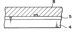
(monocrystal IA). ;
Subsequently, the surface of the monocrystal
A is flattened by etching or polishing to form a ~;~
~; monocrystal layer 8 on the thin film 5, by which a -
10 desired element can be formed, as shown in Fig. 3D or
Fig. 4B.
Thus, since the thin film 5 constituting the
non-nucleation surface (SND5) is formed on the
substrate 4, any desired material can be used for the
15 substrate 4 which is the supporting member. Further,
~-~ {n uch case, even if the substrate 4 may be one
havlng a functional element, etc. formed by
semiconductor~technique, a monocrystal layer 8 can be
ea~slly forme~ thereon.
20` ~ In the above embodiment, the non-nucleation
surface (SN~S) was formed with the thin film 5.
However, as shown in Figs. 5A - 5D, a substrate
comprising a material with small nucleation density
ND)~enabling selective nucleation may be used as
25 such, and a substrate for crystal formation may be
prepared by providing a nucleation surface (SNDL) at
' ~:' ' ` .. ~.
,; ~ .
: `
- 20 - 1332039
1 any desired position thereof.
Figs. 5A - 5D are diagrams of the f~rmation
steps of the crystal showing a second embodiment of
the present invention. As shown in Figs. 5A - 5D, by
5 forming a nucleation surface (SNDL) 6 comprising a
material with larger nucleation ~ensity (ND) ;
sufficiently finely on a substrate g comprising a
material with smaller nucleation density (ND) enabling
selective nucleation to provide a substrate for
10 crystal formation, a monocrystal layer 8 can be formed
thereon similarly as in the first embodiment.
Figs. 6A - 6~ are diagrams of the formation
steps showing a third embodiment of the process for
forming the crystal according to the present
15 invention, and Figs. 7A and 7B are perspective views
; ~
;~; of Figs. 6A and 6D. ;~
As shown in Figs. 6A and Fig. 7A, on an
~ amorphous insulating material substrate 11, nucleation
;~ surfaces (SNDL) 12-1, 12-2 are arranged sufficiently
20 finely with a material different from the material of
the substrate 11 with a distance Q therebetween. The
l distance Q may be set e~ual to or greater than the
size of the monocrystalline region re~uired for
formation of, for example, a semiconductor element or
~, ~ , .. .
25 a group of semiconductor elements.
Next, by selecting appropriate crystal forming
~: '
- 21 - 1332039
1 conditions, only one nucleus of the crystal forming
material is formed on only the nucleation surfaces
(SNDL) 12-1, 12-2, respectively. That is, the
nucleation surfaces (SNDL) 12-1, 12-2 are re~uired to
5 be formed to sufficiently fine sizes (areas) to the :~
extent that only a single nucleus may be formed. The
: sizes of the nucleation surfaces (SNDL) 12-1, 12-2,
which may differ depending on the kind of the
material, may be preferably lO~m or less, more .
10 preferably 5~m or less and most preferably l~m or
less. Further, the nucleus grows while maintaining a ~:
monocrystal structure to become isl~n~-shaped grains : :~
13-1, 13-2 as shown in Fig. 6B. For island-shaped
monocrystal grains 13-1, 13-~ to be formed, as already
15 mentioned, it is desirable to determine the conditions :
for crystal forming treatment so that no nucleation
will occur at all on other surfaces than the
: nucleation surfaces (SN~L) on the substrate 11.
The crystal orientations of the island-shaped - ::
20 monocrystal grains 13-1, 13-2 in the normal direction `:
of the substrate 11 are constantly determined so as to
make minimum the inter:face energy of the material of
the substrate 11 and the material forming the nucleus. :~
:;: ~ : : `;
: This is because, the surface or the interface energy `.,.
25 has anisotropy depending on the crystal face.
However, as a:lready mentioned r the crystal orientation `~
.
":,;,',-'
/ ~ ~
- 22 - 1 3 3 2 0 3 9
1 within the substrate plane of an amorphous substrate
cannot be determined.
The island-shaped monocrystal grains 13-1, 13-
2 further grow to become monocrystals 13A-1, 13A-2,
5 whereby adjoining monocrystals 13A-1, 13A-2 contact
mutually each other as shown in Fig. 6C, ~ut since the
crystal orientation within the substrate plane is not
constant, a crystal grain boundary 14 is formed in the
middle portion between the nucleation surfaces (SNDL)
10 12-1 and 12-2.
Subsequently, monocrystals 13A-1, 13A-2 grow
three-dimensionally, but the crystal face with slower
growth speed will appear as facet. For this reason,
flattening of the surfaces of monocrystals 13A-1, 13A-
15 2 is performed, and further the portion including thegrain boundary 14 is removed, to form the thin films
15-1, 15-2 of monocrystals each containing no grain
boundary in shape of lattice as shown in Figs. 6D and
B. The sizes of the monocrystal thin films 15-1, 15-2
20 are~dètermined by the distance Q of the nucleation
surface (SNDL) 12 as described a~ove. That is, by
defining appropriately the formation pattern of the
nucleation surface ~SNDL~ 12, the position of the
gra~in boundary can be contrblled to form monocrystals
26~with desired sizes at a desired arrangement.
Figs. 8A - 8D illustrate the steps of forming
;'
- 23 - 1 3 3 2 03 9
1 a crystal showing a fourth embodiment of the present
invention. As shown in the same Figures, similarly as
in the first embodiment is formed on a desired
substrate 4 a thin film non-nucleation surface (SND5)
5 5 comprising a material with smaller nucleation
density (ND), and a nucleation surface (SNDL) 12
comprising a different material with larger nucleation
density thereon with a distance of n to provide a
substrate, whereby a monocrystal layer 15 can be
10 formed thereon in the same manner as in the above
third embodiment.
Figs. gA - 9C illustrate the steps of forming a
crystal according to the process of the present
invention showing a fifth embodiment, and Figs. lOA
15 and lOB are perspective views in Figs. 9A and ~C. -
~ irst, as shown in Figs. ~A and lOA, a
concavity 16 with desired size and shape is formed on
an amorphouæ insulating substrate 11, and a nucleation
surface (SNDL) 12 with sufficiently fine area size
20 capable of forming only a single nucleus is formed ;.
therein.
Subsequently, as shown in Fig. ~B, an island-
shaped monocrystal grain 13 is grown in the same
manner as in the first embodiment. .
Andr as shown in Figs. gC and lOB, the
monocrystal grain 13 is gro~n until e~bedding the
- 24 - 1 3 3 2 0 3 9
1 concavity 16 to form a monocrystal layer 17.
In this embodiment, since the monocrystal
grain 13 grows within the concavity 16, the steps of
flattening and removing the grain boundary portion
5 become unnecessary.
Figs, llA - llC illustrate the steps of
formin~ a crystal showing a sixth embodiment of the
present invention. As shown in the same Fi~ures, on
any desired substrate 4 similar to the first
10 embodiment, a thin film non-nuGleation surface (SNDS)
18 co~prising a material with smaller nucleatio~
density tN~) is formed, and a concavity 16 with
: -
desired size and shape is formed thereat. And, in the
concavity is formed in a fine area a nucleation
15 surface (SNDL) 12 comprising a material which is
`~ different from the material forming the non-nucleation
surface (SNDs) and having larger nucleation density
(ND), and a monocrystal layer 1~ is formed similarly
as in the fifth embodiment.
Fi~s. 12A - 12C illustrate the steps forming a
crystal showing a seventh embodiment of the present
invention. After a concavity is formed on a desired
~ubstrate 19, a thin film non-nucleation surface
SND5) 20 comprisin~ a material with sufficiently
25 small nucleation density (ND) is formed, and
following the same procedure as in the above
~'~
`. 1332039
- 25 -
1 embodiments, a monocrystal layer 1~ can be formed.
Figs. 13A - 13D illustrate the steps of
forming a crystal showing an eighth embodiment of the
present invention.
Figs. 13A - 13C are the same as Figs. 6A - 6C.
That is, a plural number (two in the Figures) of
nucleation surfaces 12 are formed with an interval of
Q to form monocrystal grains 13 subjected to
overgrowth on the nucleation surface 12. By growing
10 further the monocrystal grains 13 to form monocrystals
13A, a grain boundary 14 is formed at approximately ;
the center of the nucleation surfaces (SNDL) 12, and ~;.
by flattening the surface of the monocrystal 13A, a
i,
polycrystalline layer 21 with grain sizes being
15 substantially regularly Q as shown in Fig. 13D can be
obtained. :;
Since the grain size of the polycrystalline :~
~ : -
layer 21 is determined by the interval Q between the ~ ;
nucleation surfaces (SNDL) 12, it becomes possible to
-~ 20 control the grain size of the polycrystal. In the
prior art, the grain size of a polycrystal was changed
~ ;depending of a plurality of factors such as the
-~formation method, the formation temperature, etc., and
when a polycrystal with a lar~e grain size is to be
25 prepared, it had a grain size distribution with a
considerable width. According to the present
~: ,' ' ~
'
: ~,
~ 1332039
- 26 -
1 invention, the grain size and the grain size
distribution can be determined with good
controllability by the interval Q between the
nucleation surfaces 12.
Of course r as shown in Figs. 8A - 8D, the
above polycrystalline layer 21 may be formed by
forming a non-nucleation surface (SNDS) 5 with ~maller
nucleation density and nucleation surfaces ISNDL) 12-
1, 12-2 on a desired substrate 4. In this case, as
10 already described, the polycrystalline layer 21 can be
formed with controlled grain size and grain size
distribution wlthout restrictions with respect to the
~: material, structure, etc. of the substrate.
In the following, specific processes for
15 forming the monocrystal layer or polycrystal layer in
the above embodiments are described in more detail.
~: Exam~le 1 :
~`:
Referring to Fig. 14, the process for forming
CdSe film on SiO2 i5 described as a first example of
~ : 20 the present invention.
`-~ First, on a substrate 4 comprising alumina, a
SiOz film 5jwas deposited to about 1000 A by the
conyentional CV~ (chemical vapor deposition) by use of
silane (SiH4) and oxygen (2)' The nucleation density
~; 25 (NDs) of CdSe on the SiO2 film i~ small, and the SiO2
film 5 forms the non-nucleation surface (SNDS). In
~ ""
- 2~ - ~332039
1 place of forming a SiO2 film on the substrate 4, the
substrate 4 per se may be constituted of a material
such as SiO2 r alumina, etc.
Next, the surface of the SiO2 film 5 was
5 masked with a photoresist to a desired pattern. :
By use of an ion implan-ter, Se ions were
implanted to the side of the photoresist-masked SiO2
film. The Se ions were impl~nted only on the surface
of the SiO2 film exposed cFig. 14A]. The amount
10 implanted was 1 x 10¹⁵/cm2. At the SiO2 film surface
where no Se is implanted, the nucleation density (N~s)
of CdSe is small, and this portion becomes the non-
nucleation surface (SND5). On the other hand, the
regions 12-1, 12-2 where Se ions are implanted have
15 larger nucle~tion density (NDL) than the non-
nucleation surface (SND5), which portions become
nucleation surfaces (SNDL). At this time, when the
size of the ion implanted portion was made 1.2 ~m
s~uare. Thus, the substrate for forming a crystal was
20 prepared.
After the photoresist was peeled off from the
SiO2 film, the substrate was subjected to heat
treatment in a PCQ3 atmosphere at about 450 C for
about 10 minutes to clean the surface.
; 25 Subse~uently, while the substrate was heated
~ to 450 C, diethyl cadmium (Cd(C2H5)2, hereinafter
- 28 - 1 3 3 2 03 9
1 referred to as DECd) and selenium hydride (H2Se) at a
molar ratio o~ 1:5 were flowed together with a carrier
gas H2 onto the substrate surface to grow a CdSe
crystal thereon according to the MOCVD (organometallic
5 chemical vapor deposition) method. The reaction
pressure was made about 20 Torr. This state was
maintained for a certain period, and then a single
nucleus was formed on each of the regions 12-1, 12-2
surfaces, and in each single nucleus the growth of a
10 single crystal started. Thus, as shown in Fig. 14B,
CdSe crystals 13-1, 13-2 was grown on the nucleation
surfaces ~SN~L) 12-1, 12-2 formed by implantation of
; Se ionst and no CdSe crystal was grown on the non-
~; . .
nucleation surface (SNDS), namely the SiO2 film
15 surface where no Se was implanted.
Growth of the CdSe crystals 13-1 and 13-2 were
~ , .
~ further continued, and the CdSe crystals 13A-1, 13A-2 ~;
`'5'.~ became to~contact each other as shown in Fig. 14C. At
that~stage, the growth of the crystals (interruption
~ 20~of crystal rorming, operation) was stopped. The
;!''i'~",`~;~ surfaces of the CdSe crystals 13A-1 and 13A-2 were
polished and the~grain boundary was etched, and then
CdSe~crystala 15-1, 15-2 as shown in Fig. 14D were
`obtained.~ A~substrate temperature was 4~0 C and a
25 reaction pressure was 30 Torr. :~
; The CdSe monocrystal 15-1, 15-2 thus obtained
- 29 - ~3~2~39
1 were evaluated by observation with an electron
microscope and X-ray diffraction. As the result, for
each of the monocrystals 15-1, 15-2, 50 x 100 CdSe
monocrystal, with grain size of 80 ~m and subtantially
5 without grain size distribution, were found to be
formed on the substrate
All of these CdSe monocrystals are shown to
have monocrystal characteristics of extremely good
quality. ::
10 Example 2
Referring to Fig. 8, a second example of the
present invention is described.
First, on the surface of a substrate 4
resistant to high temperature made of ceramics, an SiO2
15 film 5 was deposited to about 1000 A according to the
thermal CVD method by use of Si~4 and 2
Next, by means of an arc discharge type ion
platin~ device, on the SiO2 film 5 was deposited an
~;~: Al203 film. Upon the deposition, after the device was
: 20 internally evacuated to 10 5 Torr, 2 gas was
introduced to 3 x 10 4 Torr in partial pressure, and
an ionization voltage was set at 50 V, a substrate
~- potential at: -50 V and an output at 500 W. Thus, an
Al203 film was deposited to about 300 A on the SiO2
25 film 5. According to the electron ray diffraction
analysis, the Al203 film was found to be amorphous. ~:
- 30 - 1332039
1 With a photoresist masked to a desired pattern
on the Al203 film, the portion with the A1203 film
exposed was etched with an etchant of
H3P04:HN03:CH3COOH:~20=16:1:2:1 to form nucleation
5 surfaces 12-1, 12-2 (see Fig. 8A). At this time, the
substrate 4 was heated t~ about 40 C. The size of
the nucleation surface 12-1, 12-2 was made 1.2 ~m
square. Thus, the substrate for forming a crystal was
prepared.
Then, after the photoresist was peeled off,
the substrate 4 was subjected to heat treatment in a
PCQ3 atmosphere at about 450 C for about 10 minutes
2 to clean the surface. On the SiO2 surface 5,
nucleation density (NDs) of CdSe is smallr which ;
15 portion becomes the non-nucleation surface ~SNDS). On
the other hand, Al203 films 12-1, 12-2 have larger
n~cleation density (ND~) than the non-nucleation
æurface (SND5) 5, which portion becomes the nucleation
.:
rface (SNDL)
~- 20 Subsequently, while the substrate 4 was heated
to 500 C, diethyl cadmium (DECd) and selenium hydride
Se) at a molar ratio of 1:5 were flowed together
with a carrier gas ~2 onto the substrate surface to
~ :~: : .
grow a CdSe film according to the MOCVD
~;~ 25 (organometallic chemical vapor deposition) method. ~`~
The reaction pressure was made about 30 Torr. CdSe
_ 31 _ 1332039
1 crystals 13-1, 13-2 were grown only on the Al203
nucleation surfaces ~SNDL) 12-1, 12-2, and no nucleus
sufficient to grow a crystal was formed on the non-
nucleation surface ~SNDS) 5, namely the SiO2 surface.
~hen the crystal-~rowing operation was further
continued, CdSe crystals of good ~uality were obtained
similarly as in Example 1. A substrate temperature
was 470 C and a reaction pressure was 30 Torr. The
ratio of DECd and H2Se was 1:5.
10 Example 3
On the surface of a substrate resistant to
high temperature made of alumina, an A1203 film was
deposited to about 300 A by means of an arc discharge
type ion plating device.
, :
lS Next, a SiO2 film was deposited to about 1000
according to the thermal CVD method by use o~ SiH4
and 2
With a photoresist masked to a desired pattern
on the SiO2 film, the portion of the SiO2 film exposed
20 was etohed according to reactive etching by use of
CHC12F to form a nucleation surface having a part of
the A1203 partially exposed. At this time, the
substrate was heated to about 400 C. The size of the
nucleation surface was made 1.2 ~m s~uare. Thus, the
25 substrate for forming a crystal was prepared.
After the photoresist was peeled off, the
- 32 - 1332039
1 substrate 4 was subjected to heat treatment in a PCQ3
atmosphere at about 900 C for about 10 minutes to
clean the surface. On the SiO2 film surface,
nucleation density (N~s) of CdSe i5 small, which
5 portion becomes the non-nucleation surface (SNDs). On -
the other handr Al203 film has larger nucleation
density (NDL) than the non-nucleation surface ~SN~5),
which portion becomes the nucleation surface (SNDL).
Subsequently, while the substrate was heated
10 to 500 C, diethyl cadmium (DECd) and selenium hydride
(H25e) at a molar ratio of 1:5 were flowed toyether
with a carrier gas H2 onto the substrate surface to
grow a CdSe monocrystal according to the MOCVD
(organometallic chemical vapor deposition) method.
15 The reaction pressure was made about 25 Torr. A CdSe ~
crystal was grown around its single nucleus formed ~;
only on the A1203 nucleation surface ~SNDL), and such ;~
a growth of a CdSe crystal was not found on the non-
nucleation surface (SNDS), namely the SiO2 fil~
20 surface.
When the crystal-growing operation was further
c,ontinued, CdSe crystals of good quality were obtained
oimilarly as in Example 1.
Example 4
25 ~ On a quartz substrate~ a silicon nitride film
was deposited to about 300 A thick according to the
`~ :~ ',
: : `
_ 33 _ ~332039
1 plasma CVD method. At this time, H2, SiH4 and NH3
were flowed ~t the ratio of 8:2:5, and a reaction
pressure was 0.16 Torr, RF power was 10W and a
substrate temperature was 300 C.
Then, patterning was performed with a
photoresi~t. The size of the silicon nitride film was
made 1.2 ~m square. Remaining small area of the
silicon nitride fil~ becomes a nucleation surface and
the surface of the quartz substrate exposed becomes a
10 non-nucleation surface.
After the photoresist was peeled off, the
substrate was subjected to heat treatment at 900 ~C ;~
for 10 min. under H2 atmosphere to clean the surface.
Thus, the substrate for forming a crystal was -
15 prepared.
~, . . .
While the substrate was heated to 600 ~C,
diethyl cadmium (DECd) and selenium hydride (H2Se) at
a mole ratio of 1:5 were flowed together with carrier~
:
; gas, H2 onto the substrate surface to grow a CdSe film
20 according to the MOCVD (organometallic chemical vaper
deposition). The reaction pressure was about 25 Torr.
CdSe crystal was grown around its single nucleus only
formed on the silicon nitride nucleation ~urface
(SNDL). No nucleus for the growth of a crystal was
25 not formed on the non-nucleation surface, namely the -~
.~
~ ~ quartz surface. ~
~ .
~ 34 ~ ~1 332039
1 Example 5
A ZnSSe mixed crystal II-VI group compound
~onocrystal was selectively formed as below.
After deposition of SiO2 film 5 to about 1000
5 A on a substrate 4 (high melting glass) according to
the thermal CVD method by use of Si~4 and 2 in the
same manner as in Example 1, with a photoresist masked
to a desired pattern on the SiO2 film surface, Se ions ~-
were implanted into the exposed SiO2 film at 3 x
10 101 /cm2 by use of an ion implanter. The size of each
of the implanted regions 12-1, 12-2 was made 1.2 ~m
;~ square. Thus, the substrate for forming a crystal was ;~
prepared.
Next, the resist film was peeled off, and the
15 substrate was subjected to heat treatment in a PCQ
atmosphere at about 450 C for about 10 minutes to
clean the surface.
Also for the ZnSSe mixed crystal, the SiO2 -~
portion implanted with no Se ions has smaller ;`~
20 nucleation density (NDs) to become the non-nucleation
surface (SND5). On the other hand, the portions 12-1,
12-2 implanted with Se ions have larger nucleation
density (NDL) to become the nucleation surface (SNDL).
Onto the surface where the nucleation surfaces
25 (SNDL) 12-1, 12-2 and the non-nucIeation surface
:~ ~
~ (SNDs) thus having a nucleation density difference
~ '"'' ''"
:
35 _ 1332039
1 (~ND) exist, by use of H2 as the carrier gas,
dimethylzinc (DMZn), dimethylselenium (DMSe) and
diethylsulfur (DES) were flowed at a ratio of
DMZn:(DMSe~DES) of 1: iO (molar ratio). The substrate
5 temperature was made 500 C by heating. The reaction
pressure were made 30 Torr. Similarly is shown in
Fig. 14B, only on the nucleation surface (SNDL) formed
by implantation of Se ions, the ternary mixed crystal
II-VI group compound ZnSSe monocrystal was formed
10 selectively. When the crystal-growing operation was
continued, the monocrystals 13A-1, 13A-2 were grown as
shown in Fig. 14C. The size of each of the
monocrystals was about 80 ~m, and the crystallinity
was good.
In this case, the ratio of S and Se in ~nSSe
can be freely controlled by varying the ratio of the
reactive gases DES and DMSe.
.~
-- As shown above in Examples, according to the
present invention, a single nucleus is formed on a
~; ~ 20 nucleation surface (SN~L) of several ~m or less having
, .~ , ,
larger nucleation density (NDL), and a compound
semiconductor monocrystal belonging to the group II-VI
of the periodic table can be grown only from the
single nucleus.
Example 6
`:::
~ . .
- - ,13~2039
- 36 -
1 A chalcopyrite compound monocrystal with the
group II element in the II-VI group compound
substituted with the group I element and the group III -~
element is formed as follows.
Similarly as in the respective examples
described above, SiO2 film was formed on an alumina
substrate, and Se ions were partially implanted
therein similarly as in Example 1 to form a nucleation
surface (SNDL). Alternatively, as in Example 2, an
10 AQ203 film was formed on an SiO2 film, followed by
patterning to form a nucleation surface (SMDL) To the -~
substrate where the non-nucleation surface (SNDs)and
-:
the nucleation surface (SN~L) thus coexist was applied ~-
cry~tal forming treatment by the MOCV~ method to form
15 a single nucleus only on the fine nucleation surface
` ~ (SN~L), thereby forming selectively a chalcopyrite ~-
monocrystal with the nucleus being the center. In
forming the CuGaS2 monocrystal, cyclopentadienyl-
; triethylphosphine copper [C5H5CuP(C2H5)3],
20 trimethylgallium (TMG) and hydrogen sulfide (H25) were
supplied as the reactive gases together with the
. .
,~ i carrier gas H2 onto the substrate. C2H5CuP~C2H5)3 and ~ -
TMG were supplied in equal moles, with the amount of
E2S being made about several-fold of the sum of the
25 former two. The reaction pressure was made 200 Torr, ,-~
and the sub~rate temperature 550DC. Thus, a CuGaS2
~ ' .,' ~
f~
` 13~203~
- 37 -
1 monocrystal could be formed selectively on the SiO2
film.
As shown in the above Examples, according to
the present invention, only a single nucleu~ can be
5 formed on a nucleation surface (SNDL) of an extremely
fine area having a large nucleation density (NDL), and
a compound semiconductor monocrystal grown only from
the single nucleus can be formed.
In the above Examples, there are shown
10 examples in which a SiO2 film is formed by the CVD
method, but a SiO2 film can be also formed according
to the sputtering method. Further, ~uartz itself with
its surface well flattened can be also used as the
deposition surface.
The ion species to be implanted for formation
of the nucleation surface (SNDL) is not limited to Se
ions, but ions of the group II elements, ions ofi the
group VI elements, and further ion~ of the group III
elements and ions of the group V elements can be also
20 used.
By use of dimethylzinc, diethylzinc
2n(~C2H5)2], dimethylcadmium ~Cd(C~3)2],
diethylcadmium, dipropylcadmium ~Cd(C3H7~2~,
-~ ~ dibuthylcadmium ~Cd(C4Hg)2], dimethylmercury
25 ~Hg(GH3)2], diethylmercurY ~Hg(C2H5)2] ~s the starting
gas of the group II element, hydrogen sulfide (H25),
'
- 38 - ~332039 -
1 selenium sulfide, dimethylselenium, diethylselenium
~Se(C2H5)2], dimethyldiselenide ~CH3SeC~3),
dimethyltellurium [Te(C~3)~], diethyltellurium
[Te(C2H5)2], as the starting gas of the group VI
5 element, monocrystals of the II-VI group compounds
ZnS, ZnTe, Cds, CdTe, HgSe and mixed crystal compound
monocrystals thereof can be formied selectively
according to the combinations of these by forming only
a single nucleus on the nucleation surface (SN~L)
10 followed by formation of a monocrystal with the
nucleus as the center. Selective formation of a ZnO
monocrystal is also possoble. ;
The mixed crystal compound semiconductor
monocrystals can be selectively grown on the Al203 ;~
;~15 film provided on SiO2 film similarly as in Example 2
as the nucleation surface (SNDL), as a matter of
course.
Further, in the respective Examples as
described above, there are shown examples in which the
20 MOCVD method is used in the steps of selective
formation of CdSe and ZnSSe monocrystalsr but
selective formation of the II-VI group compound
monocrystal can be performed also according to the ~`
same principle by use of the MBE (molecular beam
25 epitaxy~ method, etc.
;~As described in detail above, the II-VI group
: ' '
3g 1332039
1 compound crystal article and the process for forming
the same according to the present invention, by
forming a nucleation surface (SN~L) of a material
having sufficiently larger nucleation density (ND~
5 than the material for formation of non-nucleation
surface (SN~s) sufficiently finely so as to grow only
a single nucleus, a monocrystal is grown selectively
at the site where the fine nucleation surface (SNDL)
exists, whereby a crystal such as a monocrystal with
10 necessary size, monocrystals shaped in a plurality of
islands, a polycrystal with controlled grain size and
grains size distribution, etc. can be easily formed on
a base substrate of any desired material. Besides, no
special new preparation device is re~uired, but it can
15 be formed by use of a device used in conventional
emiconductor process.
Also, the crystal according to the present
invention is not restricted with respect to the
material of the base substrate as in the prior art,
20 and therefore can accomplish easily three-di~ensional
integration, area enlargement and low cost. For
, ,~ example, since a monocrystal or polycrystal of II-VI
group compounds can be easily formed on an amorphous
insulating material, a multi-layer formation of an
25 element with excellent electrical characteristics can
~; be accomplished to realize an integrated circuit of
1332039
1 multi-functions not found in the prior art.
Specifically, it becomes possible to obtain optical
element, surface acoustic element r piezoelectric
element, etc., and integration of each of them with
5 surrounding circuit IC, etc. Also, the present
invention, when an inexpensive glass or ceramic is
used as the base material, can be applied for a large
area electronic device such as a large scale flat
panel display having the driving circuit integrated on
10 one sheet of glass, etc. .:''
Further, the present invention can form
monocrystals with necessary sizes at a plural number
of sites by forming the above nucleation surfaces
(SNDL) with desired sizes and desired intervals
15 therebetween on the non-nucleation surface (SNDS),
whereby the formation steps can be simplified to a
great extent and also the formation time shortened, as
compared with the melting solidification method in
which monocrystal is formed by irradiation of laser or
20 electron beam.
Also, by controlling the interval between the
nucleation surfaces (SNDL) to be formed on the above
non-nucleation surface (SN~S), a polycrystal
controlled in its grain size through the interval can
25 be formed. The process for forming the polycrystal is
better in controllability of grain size and grain size
1~32039
- 41 -
1 distribution as compared with the process of the prior
art in which a polycrystal of a large grain size is
for~ed according .o the above ~elting solidification
process, and also the formation time can be shortened
5 to a great extent.
~ ::
:,, ~ ' .
~;