Note: Descriptions are shown in the official language in which they were submitted.
-1- 133~ 1'?0
SWITCH ~ONITORIN~ ARRANGEMENT WITH
REMO~E ADJUSq~MENT CAPABILITY
Description
The present invention i6 directed to a monitoring
arrangement, that is, an ~rrangement for 6en6ing 60me
parameter of a ~ignal at given intervals, then processing
the result of the 6ensing, and as a result of that proces-
6ing, proYiding an indication of the parameter. In addi-
tion a signal received from outside the monitoring arrange-
ment adjusts the 6ensing operation and/or the processingoperation in the sy~tem operation.
The invention i8 useful in connection with monitoring ~
the state of a mechanical switch or analogous units in fire -~ `
and/or burglar alarm systems. For simplicity of expla-
nation a simple, two position switch will be shown and
desscribed. In general the invention is concerned with
indicating the switch state (such as open or closed) to an
as~ociated circuit. ; ~
Various types of circuits have been employed to ;
determine and indicate 6witch 6tatus. Frequently a
~`~ "debounce" circuit is used, and such an arrangement
inspects the switch condition from time to time and then
report~ on it~ 6tatus. Often the inspertion is made by
;passing a current through the ~witch. Using a continuous
current flow, the probability of error in the 6tate
~ determination i6 minimal, but this consumes considerable
i~ power. Energy is conserved by 6hortening the time during
which the current i~ pa6sed through the 6witch, but this
: ~
,~
'~
:.
~" -2- 1 332 1 90 ~
may also increase error in the state determination process,
as will be more fully explained hereinafter. It is thus
important to attain the optimum trade-off between duration
of current flow (that is, power consumption) and proper
determination of the switch 6tate.
. ~:
The inventive system operation is roughly comparable
to peeking at a 6cene or situation, and surmising from a
series of peeks what is going on. Suppose ~iomeone is
watching television, and the family cat is in the corner of
the same room. The television watcher occasionally glances
at the cat to determine if the cat is sleeping, eating, or
playing. The watcher can vary the frequency and/or
duration of the glance, and comes to an initial deter~
mination of what the cat is doing based on the results
noted during the glances. After the first conclusion is
;~ made, a further refinement can be added, such as requiring
a finite number of successive indications of the same state
to conclude what the cat is actually doing. ~his two step
procedure, an initial ~ensing and a subsequent con~
firmation, i5 helpful in gaining a perspective on the
invention described below.
-~ Many different types of circuits have been u~ed to
examine the ~tate of a given contact 6et, and report or
otherwise ignal to associated equipment what is the status
of the particular contact. One such example i8 found in
U. S. Patent No. 4,658,249, entitled "Data Communication
System With Key Data ~it Denoting Significance of Other
Data Bits", which issued April 14, 1987 to William R. Vogt,
~ the inventor of the subject matter described in this appli-
i~ 30 cation. This earlier patent depicts in Figure 7 a "moni-
~; tored contact" 66, the state of which is examined and
^-~ reported by a switch state determination arrangement 67.
~; It is to the improvement of such arrangement that the
present in~ention i8 principally directed. In
;~ .
: '^` r~,
." ,.,
~ 3 1332190
general it is desired to improve upon the arrangement of
the '249 patent by providing an improved debounce circuit
which not only provides the option of modifying operatlon
of the determination circuit, but in addition effects such
modification in accordance with a signal received from an
external source.
~ he present invention may include a trans-
mitter/receiver which is operable to receive first signals
and to transmit second signals. Switch means is provided,
either internal or external to the transmitter/receiver;
the ~witch means has at least two states. The trans-
mitter/receiver includes a debounce circuit, which is
operable to utilize a preset time period in determining the
etate of the switch means. In addition the trans-
1~ mitter/receiver includes some means, operable in responseto a received first signal, to provide a select signal to
the debounce circuit, for e~tablishing the preset time
period.
In accordance with another feature of the invention,
the ~ransmitter/receiver may include a sensing circuit,
coupled between the cwitch ~eans and the debounce circuit,
for indicating to the debounce circuit the ~tate of the
switch means. The ~elect signal is also used to modify
operation of the 6ensing circuit.
2~ Stated in another way, the present invention may be
incorporated in a communication system which utilizes a
transmitter or controller for sending the firct signals to
a plurality of receivers or transponders which both reaeive
the fir~t ~ignalE and return second signals to the
transmitter. A switch ~eans i8 provided, either within or
without at least one of the rece~vers, and this switch
means has at least two ~tates. The receiver associated
with the ~witch means includes state determination means,
coupled to that switch means, for providing a status signal
which varies as a function of the state of the switch
1 332 1 90 ~:
-4- ~
means. Also included in the receiver i8 a debounce
circuit, operable to receivs the Etatus signal from the
state determination means, and to operate upon this status ~i
signal to provide a resultant signal. Further the receiver
includes selector/controller means, which operates in
response to a first signal received from the transmitter to
provide a elect signal to the sensing circuit and to the
debounce circuit. This ~elect signal modi~ie~ both the
sensing circuit and the debounce circuit in the specific
receiver in accordance with the information received in the
first signal from the transmitter.
In the several figures of the drawings, like ~
ref~rence numerals identify like components, and in those ~ ~i
drawings:
FIGURE 1 is a block diagram depicting components of a
known communication system;
FIGURE 2 i~ a block diagram, similar to FIGURE 7 in
the earlier '249 patent, but modified to incorporate in a
general way the debounce system of the present invention~
~.
FIGURES 3A-4C are gxaphical illustrations useful in
understanding the invention; -
FIGURE 5 is a block diagram of the debounce
arrangement of the pre~ent invention;
:, .',.'
FIGURE 6 is a block diagram, partly in schematic ~
25 form, of one portion of the debounce circuit shown in ; ~-
FIGURE 5; and
FIGURES 7A-7E are graphical illustrations useful in `
understanding operation of the invention.
; - ~
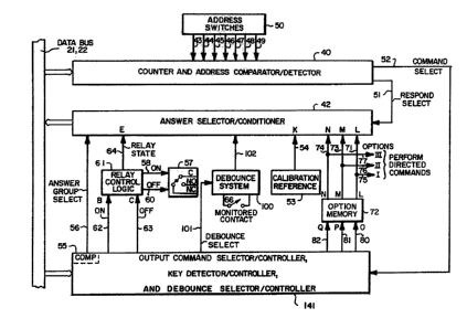
FIGURE 1 of this application deplcts a communication ~
' "''-';
,'' ' '
: 1332190
-5-
system, and is the same illustration as FIGURE 1 in the
above-identified '249 patentO Controller 20 includes a
command circuit for sending ~iignals over the data bus 21,22
to a plurality of transponder6 or transmitter/receivers
23,24 and 25. In response to these fir6t or incoming
signal6, the various transponders can initiate or return
second or outgoing signal~i over the data bus to the
controller. Othsr types of communication 6ystems are also
pertinent to the invention, as well a6i ~itand-alone
transmitter/receiver6 which provide an effective, variable
debounce as a function of a received debounce-adjust ~elect
signal .
FIGURE 2 of the present application is very similar
to FIGURE 7 of the above-identified '249 patent. However,
the ~witch state determination circuit 67 in that patent
I has been replaced in FIGURE 2 of this application by
¦ debounae system 100, shown receiving a debounce select
signal over conductor 101 and providing an output or
control signal over line 102 to the answer selec-
tor/conditioner circuit 42. The related circuit 41, in the
earlier teaching an "output command selector/controller and
key detector/controller" 41 has been replaced in the -
present application by stage 141, denoted an "output
command selector/controller, key detector/controller, and
debounce ~elector/controller". In other words, the
function of debounce ~elector/controller has been added to
the related circuitry in the earlier teaching, and for this
reason is given the reference numeral 141. Reference
numerals under 100 in FIGURES 1 and 2 correspond exactly to
th~ reference numeral6 and components identified thereby in
the '249 patent, to facilitate familiarization with the
general ~re~ in which the invention is used. A monitored
contact set 66 iB provided and coupled to debounce system
100, BO that this ~ystem can make a determination as to the
status of the contact and provide an output signal over
line 102, ultimately for return to the controller or
transmitter, denoting the ~tatus of the monitored contact.
'`I :
!3
-6- 1 ~32 1 90
FIGURES 3A through 3D are useful to understand one of
the problems associated with the trade-off between reducing
the current flow (to conserve power) in determining the
switch ~tatus, and the proper determination of that
status. FIG-~RE 3A ~hows a representation of an actual
pulse, modified by actual conditions such as line
capacitance. In the time up to tO, the solid line curve is
level indicating no pulse has been generated. At time tO
in FIG. 3B, a pulse having a steep wave front 105 is
generated. This results ~FIG. 3A) in an actual signal
having a solid portion 104 showing the voltage ri~e aG the
lines are charged. If the pulse shown in FIGURE 3B is
terminated at tl, instead of a rapid descent as depicted by
segment 106, the actual decay follows the path indicated by
15 the dasih-dot line 107 in FIG. 3A. An arbitrary inspection ~
zone denominated 108 i5 established between the dotted ~-
lines 110 and 111. Even if the monitored switch contacts ;~
were closed when the test pulse shown in FIG. 3B was
generated, the actual signal tlO4,107) would not rise to
the lower limit of the inspection zone, thus giving an
erroneous response. `~
.. ~
FIGURE 3C shows a pulse of the same amplitude but ;;- -longer time duration, from tO to t2. This means that the -~
pulse of the same amplitude would continue past segment 104
and include segment 112 in FIGURE 3A, and at time t2 this
segment would begin to decline toward zero as shown by the
broken line 113. It i6 noted that the segment 112 extends
into the inspection zone, but not for a very significant
pdrtion of that zone. This means that a determination can
be made that the pulse segment 112 entered the zone,
indicating switch status, but there is not a significant
margin for error because of the limited extension of the
pulse seg~ent into that zone.
If the pulse duration i6 made for a longer time
interval, such as from tO to t3 as shown in FIGURE 3D, then
the lines can charge up even more so that the pulse charge
.::
d i~
~ 332 1 ~0
--7--
continues through the ~egment 114 before it begins to
decline over the segment 115. This means that the deter-
mination can be made that the pulse was of a sufficient
duration to ~ake a determination that it entered the
inspection zone, with a greater margin for error than is
the case for the pulse duration shown in FIG. 3C. However
the trade-off is that more power is expended with the
signal shown in FIG. 3D.
FIGURES 4A, 4B and 4C depict different ways in which
the pulse width and the pul~e interval can be varied, to
help compensate for factors 6uch as line capacitance, noise
on the line, and ~o forth. In FIG. 4A two brief duration,
closely spaced pulses are shown followed by a pulse
~nterval extending for a somewhat longer interval than that
of the two pulses themselves. In FIGURE 4B the same pulse
interval is maintained as contrasted to FIGURE 4A, but the
pulse width is approximately tripled. From the explanation
given in connection with FIGS. 3A-3D, it is evident that
; the extended on time in FIG. 4B allows more time to let the
pulse rise into the inspection zone. FIG. 4C shows a
different pulse train with an extended pulse interval as
contrasted to the ~howing in FIGURE 4~
j~ Those skilled in the art will understand there is no
such thing as a "pulse" or "pulse train", in the abstract.
Rather waveforms ~uch as those shown in FIGS. 4A-4C
represent variations in voltage, current, or some other
parameter of a signal which can be produced and later
measured. It is in that sense that the term "pulse" and~or
"pulse train" i5 used herein and in the appended claims.
FIGURE 5 depicts the various components of debounce
system 100. Major components are a sensing circuit 120 and
a debounce circuit 130, coupled in series between a switch
66 and the output conductors which pass the debounced
signal to the answer selector/conditionex 42, for
cooperat~ng in regulating the transmission of a signal to a
1 332 1 90
- 8 -
:
controller or to eome other unit. In a ~eneral way sensing
circuit 120 performs the "peeking" function described
generally above, to estimate the 6tatus of something, and
debounce circuit 130 provides the "confirmation" of the
initial status estimate produced by the sensing circuit.
In more detail, conductors lOla and lOlb, which
receive the debounce ~elect signal from ~elector/controller
141, are connected to a timing pulse generator circuit 117,
which includes a clock pulse generator circuit 118, a
circuit 119 for adjusting the pulse width provided on
output line 121 as a function of the debounce 6elect
signal, and another circuit 122 for adjusting the interval
between pulses of the train of pulses provided on output
line 121, also as a function of the debounce select
signal. Such circuits are well known and understood in the
art, and are easily implemented with off-the-~helf
components. The output signal on line 121, termed the
sampling clock slgnal, ~s applied to sample circuit 123 to
regulate the times at which the ~amples of (or "peeks" at)
;20 the status of switch 66 are provided. An end-of-line
resistor 124 is coupled in series with switch contact set
66, to reduce the current flow through this circuit when
the switch is clo6ed and the sample circuit 123 is
evaluating the position of the switch by sending a current
through the switch.
Sample circuit 123 provides a normal output signal on
line 125, or an alarm output signal on line 126, or a
~ 'trouble output signal on line 127, depending on the statu6
;~of ~witch 66 and its associated components. For example if
~30 the current flow assessed through the 6witch circuit falls
-~in an expected range, a normal signal could be provided.
If the current flow is excessive, it could indicate an
alarm condition. A 6ignal measured below the expected
normal state would indicate some type of trouble.
Provi6ion of the 6ample circuit and the various outputs
f ~ indicating the state determination of switch 66 are well
1332190
known in this art, and it is sufficient to indicate that
the identified state signal ie passed to one of the
individual latches within a latch circuit 128.
This latch circuit includes individual latches 129,
131 and 132. Each latch is a simple circuit such as a
flip-flop which is changed in 6tate when it receives an
appropriate signal on one of the input lines (125, 126 or
127) at the same time that a sampling clock signal is
passed over lines 121 and 133 to the three latch circuits.
Accordingly only one of the latches 129, 131 and 132 is
indicating a positive or identified signal output on its
appropriate output conductor 134, 135 or 136 at any one
time. These signals are in turn passed to the respective
debounce counters 137, 138 and 139 in debounce circuit
130. It is noted that the debounce select signal, on lines
lOla and lOlb, is passed not only to the timing pulse
generator circuit 117 utilized in the 6ensing circuit 120,
but also to the counter output select circuit 140 which is
a portion of debounce circuit 130. Counter output celect
circuit 140 utilizes the debounce select signal to provide
a preset time period by indicating an appropriate signal on
the respective one o~ it6 output conductors 141, 142 or
143. These slgnal6 are termed fast, normal and 510w in the
present arrangement. The fast ~ignal on line 141 is pas6ed
to each of the debounce counters 139, 138, and 137, and
likewise the normal and elow control ~ignals, when provided
by circuit 140, are al80 ~pplied to each of the debounce
counters 137-139. This insures that the appropriate one of
the debounce counters --- depending on which one has an
identified signal appearing on its respecti~e input
conductor at the time --- will be controlled in the preset
time period determined by counter output select circuit 140
to provide on one of the output conductors 144, 145 or 146
the appropriate debounced signal to one of the latches in
the last state memory circuit 147. These latches are latch
148 in the normal line, latch 150 in the alarm line, and
lSl in the trou~le line. Depending on which of these
1 332 1 90
--10--
latches i8 indicating an output slgnal, that signal is then
applied over the re6pective one of output conductor~ 102a,
lQ2b or 102c to answer selector/conditioner circuit 42 to
assist in generating the appropriate return signal from the
transponder to another unit in the communication
arrangement.
In operation, if the debounce system 100 is in a
stand alone environment, it is controlled by an incomin~
ignal, which in the illustrated embodiment is decoded in
debounce selector/controller 141. In a communication
system this signal is received from a transmitter, over the
air, over a data bus, or through some other communication
path. The decoded output of stage 141 provides the
debounce select signal on lines lOla and lOlb for regu-
lating both the 6ensing operation in circuit 120 and theconfirmation process in debounce circuit 130. Those
skilled in the art will appreciate that, if the option
memory 72 (FIG. 2) and its associated circuitry were not
used in a given embodiment, then the debounce select signal
could be derived from conductor~ 80,81.
The debounce ~elect signal applied to the timing
signal generating circuit 117 (FIG. 5) is effective to
establish the 6ampling clock signal on line 121. This
signal is similar to those 6hown in FIGURES 4A-4C, and the
pulse width can be modified by circuit portion 119 and the
pul6e interval modulated by pul6e interval circuit 122.
This provides the variation6 ~llustrated in FIGURES 4A-4C.
The sampling event occurs at the termination of a pulce, as
the 6ignal goes low. Inspection of FIGURES 4A-4C indicates
how the "peeks" can thus be varied in accordance with the
debounce eelect signal.
The state determination signal appears either as a
normal status signal on line 125, or an alarm signal on
conductor 125, or a trouble status signal on line 127. It
is evident that the st~tus eignal provided on conductors
1 332 1 ~CI
125-127 varies a~ a function of the 6tate of switch 66. In
addition the ~ignal varies as a function of the debounce
select ~ignal because the ~ampling clock signal i~ modified
and thus the state determination i8 made differently with
changes in the debounce selact ~ignal.
Once the initial state determinat~on i6 made, the
status signal i5 presented, through the latch circuit 128,
to the inputs of the counters 137-139 in debounce circuit
130. The counters also receive the ~ampling clock 6ignal
over line 165. A~ will become evident in considering FIG.
6 hereafter, instead of individual counters the debounce
circuit can include shift register circuits to provide the
different preset time periods for fast, normal or slow
operation. This results in an output signal on one of the
conductors 144-146, which is passed through the last state
memory circuit 147 to control the output from the receiver
or transponder as previously described. With this
perspective, the debounce circuit of FIG. 6 will now be
described.
;~ 20 FIGURE 6 shows a debounce counter 138, one of the ~ -~
three circuits depicted in debounce circuit 130. A
conventional shift register circuit forms counter 138, and
an additional flip-flop stage 170 is connected to receive
the alarm-indicating signal over conductor 135 and the
samplins clock signal over line 165. When latch 131
(FIG. 5) provides a positive indication of an alarm, at the same
time the sampling clock signal on line 121 (FIG. 6) goes low, a -
count is registered in 6tage 170. Each eubsequent~count i~
thus clocked through the register including ctages
~ .
172-177. Two additional stages (not shown) are connected
between 6tage 176 and stage 177. Whenever there is no
alarm indicat~d on line 135, inverter stage 178 provides on
line 18~ a regi6ter-clearing signal, and counter 138 is
reset to zero.
:- ' :~-' .
~`~ 35 A first AND ~tage 181 receives the output of register ~ ~
. .
-12- 1 332 1 90 ~: :
stage 1~3 and a "fast" signal over line 141 from the
counter output 6elect stage 14 0, which includes a
one-of-three selector 152. A memory 6tage 153 i6 connected
in stage 140 to receive the debounce select signal over
conductor~ 101a, 101b, and provide over conductors 154 and
155 a signal indicating the eelected speed to the
one-of-three ~elector 152. If the "fast" E;tate is
selected, then the output of regi6ter 173 i8 clocked from
AND circuit 181 (when the signal is present on line 141),
over line 156 and through OR gate 157 and conductor 145 to
signal that an alarm condition has been confirmed in the
fast operation mode.
If the "normal" mode has been selected then AND gate
:: 158 receives the output state of register 145 and, coin-
cident with the signal on line 142, provides an output over
:~: line 160 to another input of OR stage 157. In the "slow"
mode, the entire register must be filled so that the output
`~ of stage 177 is passed through AND gate 161, when a signal
;~; is present on line 143, and over line 162 to OR gate 157.
It is thus evident that the debounce circuit utilizes a
preset time period, fast, normal or slow in the described
embodiment, to provide an output signal connoting the state
, ~ .
of switch 66. This preset time period is established by
the debounce 6elect signal received over lines 101a and
101b, which determines the fast, normal and slow modes, in
turn setting how many consecutive alarm signal
confirmations must be received over line 135 before an
"alarln-confirmed" output signal is passed over line 145.
The operation of the debounce counters 137, 138 and
139 ~can be visualized in connection with FIGS. 7A-7E. In
FIGURE 7A a confirmed alarm signal iB shown, of the type
that might be presented at the output eide of latch 131 and
passed to debounce counter 138. This is the signal being
sampled. FIGURE 7B depicts the clock sample rate, that is,
a series of pulses occurring at a freguency detennined by
` ~ the debounce select signal on conductors 101a and 101b,
13~1 CJ~
-13- -
ultimately used to provide the sampling clock signal on
conductor 121. The debounce select signal is also used,
through counter output ~elect circuit 140, to determine how
many consecutive samples must be obtained to provide an
indication of the actual state. FIGURE 7C shows the output
derived when two consecutive clock samples are required to
indicate the 6tate of the signal in FIGURE 7A. This is
analogous to fast operation of the debounce counter, with
the 8ignal being clocked out of AND circuit 181. FIGURE 7D
depicts the signal produced when four consecutive samples
are required, and is analogous to normal operation of the
debounce system. FIGURE 7E depicts the output when eight
consecutive l~ke samples are required, similar to slow
operation in which the output i6 cloc~ed through AND
circuit 161 to provide the output signal. Thus it is
evident that a considerably different output waveform can
be derived from a given signal being sampled, depending
upon whether fast, normal or 610w operation is dictated by
the debounce select signal and the other portions of the
~ystem of this invention.
The present invention provides a system with positive
determination of a switch state, made from a unit which
receives a remote signal indicating the manner in which the
switch status will be determined. In a preferred
~ 25 embodiment the switch 6tatus is first sensed or "peeked
i~h~ ~ ~ at", forming the initial switch determination output
signal. In turn this initial determination is monitored by
an adjustable rate confirmation circuit, to determine the
status of the switch being monitored. Both the sensing and
the debounce functions are regulated from a signal received
remotely,~ either from a controller in a communication
system or from so=e~other source through a given communi~
oation path. If desired the 6ampling signals such as those
shown in FIGS. 4A-4C can be alternated in polarity, so that
~; 3~ by paasing the d-c current through the switch and asso-
ciated components in opposite directions, a more precise
evaluatlon of the ~yste= can be provided. The polarity
1332190 :
-14-
alternation function can be included in pulse generating
mean6 117.
It i8 important to note that the present system is
particularly useful with life and property protection
systems, such as fire alarm systems and burglar alarm
systems. The invention provides the advantages of d-c
monitoring of a pulse state, but without the power loss
conse~uent upon use of continuous d-c current flow. The
various controllable operating parameters also accommodate
different system configurations and conditions. In the
theoretical world the pulses can be considered as perfectly
rectangular, that is, having straight leading edges and
perfectly perpendicular trailing edges, but in practice,
every line has some measurable capacitance and noise
intrudes upon every system. The noise tends to come in
bursts or in a concentrated series. By allowing both the
sensing circuit and the debounce circuit to be varied as to
~the initial sensing and subsequent confirmation functions,
- a more reliable determination can be made and the system
~20 can be accommodated to various noise, capacitance and other
t'~ system fluctuations.
In the appended claims the term "connected" means a
~`~d-c connection between two components with virtually zero
d-c resistance between those components. The term
~25 "coupled" indicates there is a functional relationship
r'-" ' '~between two components, with the possi~le interposition of
air or other elements between the two components described
asincoupled" or "intercoupled".
, .
While only a particular embodiment of the invention
ha6 been de~cribed and claimed herein, it is apparent that
various modifiaations and alterations of the invention may
be made. It is therefore the intention in the appended
claims to cover all such modifications and alterations as
may fall within the true spirit and scope of the invention.
~,,