Note: Descriptions are shown in the official language in which they were submitted.
1332~37 : :
-1- '
BREAKERLESS IGNITION SYSTEM WITH ELECTRONIC ADVANCE
Backqround of the Present Invention
The present invention relates to a breaker~
less ignition system with an automatic electronic
S advance circuit and particularly to such an ignition
system in which advance changes over a wide range of
speed, between a low speed retard timing and a high ~ -~
speed advance timing.
Ignition systems for internal combustion
engines have been developed using solid state
technology which eliminates the necessity of mechanical ;~
switching devices for establishing the properly timed
firing pulse to the internal combustion engine. In the
solid state system, a voltage sensitive transistor or
lS other solid state switch responds to the ignition power
supply, which is operated in synchronism with the ~-
engine. In many relatively small and low horsepower
internal combustion engines, a magneto unit is the
source of power for the ignition system. The output of
~ 20 the magneto unit is generally a periodic alternating :
:-~ current AC signal generated in synchronism with the
. ,, . ~ :
engine operation. Thus, as the magnet moves past the
winding the signal is generated which includes three
.,
half cycles which alternate about zero or reference
level. The shape and configuration of the AC signal
vary with speed, and in particular, the magnitude and
frequency of the AC signal vary with speed. Generally,
the leadlng and trailing portions of each signal have a
lower amplitude than the central portion or half ~;
~` 30 cycle. Further, the AC signal is synchronized with the ~-
rotation of the engine, such that the time position of
the signal is directly related to the position of the
piston and the desired firing cycle of the engine.
,`~ This phenomena is known and used to provide
~ 35 automatic changes in the angle of firing in the
,~ ,~ : '"
, ...
13~2437
--2--
ignition system. Generally, the syste~ is designed to
provide a relative retard angle of firing at starting
and low speeds. The firing angle advances with speed
to provide optimum engine operation. For example, U.S.
patent 3,504,373 which issued March 31, 1970 provides a
solid state ignition switch system which has an
automatic advance with a firing just before the peak
level is obtained. Other solid state ignition systems
with various controls are shown in the following U.S.
patents:
Patent No. Issue Date Inventor
3,504,373 03/31/1970 Strelow
3,938,491 02/17/1976 Mazza
4,130,101 12/19/1978 Jundt et al
15 4,178,892 12/18/1979 Podrapsky
4,233,951 11/18/1980 Take
4,452,199 06/05/1984 Andreasson
Although various solid state ignition systems
have been disclosed, the cost and reliability,
particularly with repeatability of system operation,
have not been totally satisfactory. This is
particularly true for the smaller internal combustion
engines where the ignition system module is mounted in
a relatively confined space and may be subjected to a
wide range of temperatures during normal system opera-
~- tion. The modules are optimumly designed as small and
highly compact modules which can be mounted in the
system. Because of the wide temperature ranges
~, encountered, the circuit must be typically stabilized
to operate with a range of -40 degrees Fahrenheit (F)
to +200F. Further, the small engine market is highly
competitive and minimizing of cost is a significant
factor in producing a satisfactory competitive system.
The range of timing change is peferably from
a relatively large angle of retard at starting and low -
1 ~ 3 ~
-3-
, ,
engine speeds to an angle of advance at high normal
operating speeds. The timing angle should therefore
move from the descending or trailing side of the peak
current signal at low engine speeds to the advance or -
leading side thereof at high engine speeds. Applicant `
does not know of an ignition system which provides a ~-~
range beginning in a relatively extreme initial retard
portion of the AC ignition signal and at high speed
extending beyond the peak to a significant advance
position, thereby producing the desiràble wide change
range of the timing angle.
Further, any system which is designed would
necessarily demand a simple, compact construction at a
competitive low cost, and producing a consistent,
repeatable functioning with changes in speed. ;
Summary of the Invention -~
The present invention is particularly
directed to an automatic advancing breakerless ignition
system using an AC type signal source to produce a
relatively large retard angle during low engine speed
and an automatic advance in the timing angle with -~
increasing engine speed, with the advance moving past
the peak value of the AC signal at normal engine
operating speeds. The circuit is formed of reliable
and readily commercially available components to ;
produce an economically packaged compact module, with a
high degree of temperature stabilization and ;~ -
consistent, repeatable functioning.
Generally in accordance with the teaching of
~ 30 this invention, the magneto or other similar AC power
I; supply is connected to a primary winding and generates
a firing pulse during an appropriate half cycle of the
AC supply which is synchronized with the engine opera- ;
~; tion. The conductive path for the primary winding `
~; 35 includes a high gain switching power transistor unit ;~
~: , .... ` -
,' "'
'.": :~ '.
1332~7
-4~
such as a Darlington transistor connected essentially
in parallel with the primary winding, and particularly
includes a voltage dropping means such as a resistor or
diode in the collector circuit of the power
transistor. An input bias circuit for the power
transistor is also coupled to the primary winding, and
the power transistor is biased to conduct, thereby
providing a relatively low resistance current path
which is stabilized by the special collector voltage
dropping means. A solid state control switch such as a
control transistor is connected to the bias circuit of
the power transistor, and includes a capacitive branch
connected in an input circuit of the control switch.
The input circuit of the control transistor has one
input subject to the capacitor voltage while the
opposite side of the control transistor's input is
connected to a voltage proportional to the input bias
voltage for the high gain power transistor. The
capacitor is connected in the input circuit to charge
to a level somewhat below the peak level of the supply
signal from the synchronized AC power supply. During
the charging cycle, the capacitor charges to a maximum
' value slightly less than the peak signal of the
magneto. The capacitor voltage is applied to the
1 25 control transistor to bias it into conduction.
However, the control transistor is held off as the
result of the application of bias voltage from the
input bias circuit to the opposite side of the control
~; transistor. After the peak voltage level is reached,the capacitor voltage is maintained as the result of a
~;~ diode or other unidirectional conducting unit. The
~; voltage applied to the opposite side of the control
1~ transistor decreases as the AC supply current
;~ decreases. At a selected value, the latter voltage
~ 35 drops to a level whereby the differential input signal
..,
1332~37
across the control transistor is such that the control
transistor switches on. The control switch immediately
develops a by-pass path for the input bias signal of
the power transistor which turns off and effectively
establishes an instantaneous opening of the charging
circuit to the primary winding. The opening of the
primary winding charging circuit terminates current
flow through the inductor, with a resulting induced
high voltage which is coupled through a transformer
means to the engine firing unit such as a spark plug.
As the speed increases, the differential voltage signal
continuously advances and increases to a differential
firing level at an earIier period in the signal. The
collector impedance of the switching power transistor
serves to enhance the ignition circuit operation by
increasing the control circuit voltage with increasing
current. At normal high speed engine operation, the
capacitor voltage charge level and the back bias level
reach a differential turn-on signal prior to the peak
of the inductor current. Thus, at the advance limit,
the circuit establishes ignition prior to the peak
current in the inductor charging circuit. This
produces a maximum and significant advance firing
angle.
More ~articularly in accordance with one ~;
embodiment of the present invention, a Darlington power
, transistor is connected in series with a collector ! ';,',~':'
, resistor of a relatively low value or a forward biased -~.~ diode to stabilize the system of operation. The turn-
on signal to the power Darlington includes a pair of
series resistors connected between the base of the
power Darlington and the high potential side of the
primary winding. The control switch for the power
transistor may include a high gain cut-off transistor
connected between the junction of the input bias
s~
1332~7
resistors and the return or common connection between
the Darlington power transistor emitter and the primary
winding. A capacitor is connected to one input of the
control switch. A diode and charging resistor are
connected in series between the capacitor and the top
side of the primary winding. The several resistors
function to stabilize the system operation and produce
a repeatable temperature stable circuit.
In an alternate construction, the control
transistor has its emitter coupled to the emitter of
the Darlington power transistor with a common emitter
biasing resistor connected to the bottom side of the
primary winding.
As the primary winding current pulse
lS increases, the capacitor is charged to slightly below
the peak voltage level of the input signal, with the
capacitor voltage and the bias voltage applied across
the input of the control transistor and with the bias
voltage back biasing the control transistor. After the
pulse peak is reached, the level of the bias voltage
decreases. At lower speeds, the capacitor voltage is -~
held at a fixed level while the bias voltage decreases,
until the differential voltage appearing across the -~ -
control transistor triggers and turns on the control
transistor thus turning off the power transistor and
generating the voltage pulse across the primary winding
for firing the engine.
The control switch in one practical circuit
; consists of a regenerative circuit including a PNP
control transistor having its emitter connected to the
capacitor and its base connected to the bias circuit
resistors of the power Darlington transistor. An NPN
~ cut-off transistor has its base connected to the
,~ collector of the PNP transistor and its collector-to-
~; 35 emitter circuit connected between the connection of a
,.
'j3,
1332~7
Darlington bias circuit and the common line. A
resistor advantageously may also be connected across
the base-to-emitter circuit of the NPN transistor.
In the alternate circuit construction with
the common emitter resistor, a single control
transistor is used with the collector and emitter
connected, respectively, to the junction of series
connected bias resistors of the Darlington power
transistor and the emitter side of the common emitter
resistor. The base of the control transistor is ;
connected directly in series with a resistor to the ;~
junction of the capacitor and the charging resistor.
The charging circuit preferably also includes a Zener
diode. The common emitter circuit has a slightly
smaller cranking retard firing-angle but typically
provides a flatter temperature compensation ;
characteristic. -, ~;
Thus, with the cascaded transistor control
switch circuit, the output may vary with a range of ~
approximately 15% over the operating temperature of 0F ;-;
to plus 175F. The cut-in speed of the circuit varies
by approximately 65 rpm. In contrast, the common
emitter circuit has an output variation of only
approximately 4% during the same temperature range and
the cut-in speed varies by a minimal 25 rpm. The
cascaded transistor circuit provides a somewhat greater
ignition retard, generally on the order of an
additional two degrees. Generally, the lesser cost and -~
simplicity of the circuit using the common emitter
circuit design, particularly when combined with similar ~;
engine operation over the complete temperature range,
~j provides an economical and commercially acceptable
ignition system.
In still another alternate embodiment, a full
wave bridge rectifier including diode elements or other
1 ,. -
~''
(
1332~7
--8--
unidirectional conducting elements connects the primary
winding of the magneto unit to the power transistor
unit. At least one of the diode elements is connected in
series with the collector in place of the collector
resistor to similarly introduce a voltage drop into the
circuit. A coupling resistor is connected between the
primary winding and the cut-off or control circuit and the
input bias circuit of the power transistor unit. A
coupling diode or the like element by-passes the coupling
resistor during the negative half cycle and supplies
current to the control circuit. The resistor isolates the
control circuit from the primary winding and rectifier
output during the negative half cycle. This embodiment
functions in the same essential sequence as the previous
embodiments but over a wider angle of rotation of the
engine. Thus, in the modified circuit current flow
through the primary winding is applied to the control
circuit to extend the effective range of control. With
this circuit configuration, a step function can be
introduced into the timing characteristic as the speed
increases.
Accordingly, in one of its broad aspects, the
present invention relates to a breakerless ignition system
for or an internal combustion engine, comprising a
generator having a rotating magnet means periodically
coupled to a primary winding and generating an alternating
current output including a leading pulse signal and a
following pulse signal of opposite polarity interconnected
to form a periodic output signal and operable to generate
, 30 a firing voltage pulse upon interruption of said output
signal, a switching power transistor means having a
; collector and an emitter and an input base, a control
switch means connected to said input base to turn said
'
-8a- 1332~7 1:
power transistor means off, a voltage dropping means 1:~
connected in series with said collector to enhance system
operation at low engine speeds, and a full wave bridge
rectifier with diode elements connected between said
primary winding and said collector-to-emitter of said
power transistor means, said voltage dropping means being
one of said diode elements connected in series with the :
said collector and introducing said voltage drop into said
circuit. v~
In a further aspect, the present invention :
relates to a breakerless ignition system providing a
progressive advance in ignition timing for an internal ~.
combustion engine and having a generator operated in ; .
synchronism with the engine for generating current pulses ::
in a winding, comprising an ignition circuit having first -:~
and second power input terminals for connection to the.`~
opposite sides of said winding, a charging branch circuit :
connected to said input terminals and including a power .
switching transistor means having a collector and an
emitter and a base, said branch circuit including a . ~ -
collector voltage dropping means connected between the
I collector and the connection to said input terminals to
¦ increase the system voltage across said charging branch
~ circuit, an input bias circuit including at least first
3 25 and second resistors connected in series between said
power switching transistor and said input terminals, said ~
emitter being connected to said second terminal, a control : -
switch means connected between said bias circuit and~said .`~
second terminal and operable to turn off said power
I transistor means, said control switch means having first
~: and second input bias terminals, a capacitive control
~; circuit connected to said input power terminals and .
'! including a diode means connected in series with a
,~, .
., : .
~ii
~.l.. ` :
,.~
.;,i
... .
., .
~ 1332437
-8b-
charging resistor and a capacitor, said capacitor being
connected to said first input bias terminal of said
control switch means, resistor means connecting said
second input bias-terminal of said control switch means to
said input bias circuit of said power transistor means
with the voltage on the transistor decreasing subsequent
to the peak of the current whereby the level of the input
bias circuit voltage progressively decreases and said
capacitor voltage turns on said control switch means at a
time dependent upon the output of the generator and
functioning to terminate conduction of said power
transistor means and thereby interrupting current flow
through said winding with a progressing advance in timing
with increasing engine speed, said current interruption
generating a high pulse voltage adapted to fire said
internal combustion engine.
In still a further aspect, the present invention
relates to a magneto ignition system comprising a magneto
having a primary winding and a rotating magnet coupled to
said primary winding, said magneto having an input means
for coupling to an internal combustion engine and
operating to move past said primary winding for firing of
each cylinder of the engine, a power transistor switch
having a collector and an emitter and an input base, a
diode connected in series with said collector to the
:~ positive side of said primary winding, said magneto
generating an alternating signal in said primary winding
including a following current pulse and a leading pulse, ~-
said leading pulse having somewhat lower amplitude than
.~ 1 30 said following pulse at the operating speeds of the
engine, both of said pulses increasing in amplitude and
frequency with speed, a second diode connected in series ~:
with said emitter to one side of said primary winding to
~ .
.,'
~ :
~ , -:
~ ~:
1332~37 :~
-8c-
provide rectified current flow from the primary winding - .
through said power transistor switch, a third diode .
connected between one side of said primary winding and ~ -
said collector, a fourth diode connected to the emitter ~
and to the other side of said primary winding to establish -:
current flow through said primary winding and said third ~. :
diode through said power transistor switch, a coupling ::.
resistor connected between said other side of said primary ~.
winding and the input bias circuit of said power
transistor switch, to supply a turn-on signal to said
power transistor switch during the following half cycle of
said magneto output, a diode connected between the
collector of said power transistor switch and said bias ~- :
circuit to provide turn-on current to said power ~ :
. 15 transistor switch during the leading half cycle of said ::magneto output, a control switch means connected to the
input bias circuit and operable to bypass said input bias
circuit to terminate conduction of said power transistor
switch, said control switch means having means connecting
a timing capacitor to said input bias circuit, said
control switch means having a first input element ~ :
connected to said timing capacitor and a second input
element connected to said input bias circuit whereby the - ;
turn on of said control switch means is determined by the
relative voltage output of said input bias circuit and
said capacitor voltage, whereby said control switch means
is biased on and establishes cutoff of said power
transistor with creation of a firing pulse signal, said
firing pulse signal being created during the period the
! ! : 30 ~ primary winding current decreases after reaching its peak
value at starting and low speeds and progressively :
increasing with a gradual advance in the ignition system
firing throughout the engine starting speed range and
.~
-8d- 13324~7
includes a maximum advance established prior to the peak
current value.
The present invention provides a relatively
simple electronic ignition circuit having an automatic
operation between cranking and low speed up to and
including normal operating speeds. The circuit includes
standard components which are readily commercially
available and which reliably operate in the environment of
lawn and garden equipment, industrial equipment, marine
outboard motors and the like.
,
8rief Description of the Drawings
The drawings furnished herewith illustrate the
best mode presently contemplated by the inventor for
carrying out the invention.
' :............. ... .............................................................. ,
~ i, ~ ' ..
/. ~
, ~ ,
, . .
1~32~37
g
In the drawings:
Fig. 1 is a schematic diagram illustrating an
automatic electronic advance circuit for a magneto
driven ignition system of an internal combustion
engine;
Fig. 2 is a diagrammatic illustration of a
magneto output signal, with the vertical axis
representing signal amplitude and the horizontal axis
representing rotation angle;
Fig. 3 is a schematic circuit illustrating a
modification to the circuit of Fig. l; and
Fig. 4 is a schematic circuit illustrating a
third embodiment of the present invention.
Description of the Illustrated Embodiment
Referring to the drawing and particularly to
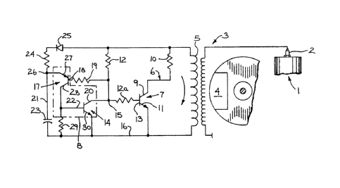
Fig. 1, the internal combustion engine 1 is diagram-
matically illustrated having a single spark plug 2.
Firing power for spark plug 2 is derived from a magneto
unit or generator 3 having a rotating magnet 4 coupled ;
20 to and driven in synchronism with engine 1, and
particularly the position of the engine piston (not
shown). The magneto generator 3 includes an inductive
primary winding 5 coupled to the rotating magnet 4.
Rotation of the magnet 4 past winding 5 generates a
25 magnetic flux through winding 5 which in turn creates a
current flow in winding 5 and an associated branch
circuit 6 connected directly across winding 5. A power
i switching transistor 7 in branch circuit 6 is biased by
~; the signal from winding 5 to conduct current through
30 winding 5 and thereby inductively charge winding 5. A
control switch unit 8 is operable conjointly with
branch circuit 6 to turn off the power switching -
transistor 7 essentially instantaneously. As is well
known, opening the circuit of a current in a highly
~; 35 inductive circuit results in generation of a voltage ~
~,:
.
1332~3~
--10--
pulse across inductor winding 5. By transformer
action, the voltage pulse is amplified and applied to
spark plug 2 at the appropriate time in the engine
cycle to ignite the fuel and power the engine, and
thereby establish and maintain operation of the
internal combustion engine. The magnet 4 rotates with
the engine, and the coupling thereof with winding 5 is
timed to çoincide with the time in the engine cycle
that the piston is in the optimum position for firing,
in accordance with conventional construction of such
engines. The firing point or time changes with engine
speed for optimum firing.
The internal combustion engine and the
magneto unit as such may be of any known or desired
construction. Such engines are readily available and -
the specifications and constructions are well known.
The present invention is particularly directed to the
ignition circuit including the charging circuit and the
firing control circuit to produce an automatic timing
and optimize the creation of the firing pulse to the
engine. Consequently, the engine and the magneto are
only described in such detail as necessary to clearly
explain and set forth the functioning and operation of
the novel and unique ignition circuit.
The power switching transistor 7 connected in ;
branch circuit 6 is a high gain, rapid acting switch,
and preferably is a temperature stablized Darlington ~ -~
transistor unit. Darlington transistors are readily -
;~ commercially available from various manufacturers
including Motorola of Illinois, NEC of Japan and
others. The Darlington power transistor 7 is ;
,~ schematically illustrated as an NPN transistor
configuration connected across inductor winding 5.
Transistor 7 has its collector 9 connected to the one
35 ~ side of winding 5 in series with a special stabilizing
: . ' '
1~324~7 ~ ~
resistor 10. Emitter 11 of transistor 7 is shown
connected directly to the opposite or common end of
winding 5. A pair of bias resistors 12 and 12a are
connected in series between the high potential side of
winding 5 and base 13 of transistor 7. As magnet 4
moves past winding 5, it generates an increasing
alternating current signal in winding 5. The frequency
and ampli,tude of the AC signal are of course directly
proportional to the rotational speed of magnet 4. The ;
AC signal is therefore also position-related to the
engine cycle and particularly the cyclical movement of
the piston (not shown). The AC signal therefore also
provides a reference signal for firing of the internal
combustion engine, as well as the power to fire the
engine.
Control switch unit 8 is coupled to inductor ~;~
winding 5 and i5 driven therefrom to control the
ignition, with a variable timing for optimum engine
operation. Control switch unit 8 is shown as a ;~
cascaded transistor circuit including a first cut-off
transistor 14, and a second control transistor 17.
Cut-off transistor 14 is shown as an NPN transistor
having its collector 20 connected to the junction or
node 15 of resistors 12 and 12a and thereby to base 13
of power transistor 7 and its emitter 30 connected to a ~ ;
common return line 16. When cut-off transistor 14 is
turned on it effectively grounds base 13 of power ! ~.
transistor 7 and drives transistor 7 off. Cut-off
transistor 14 is driven by a control transistor 17, the
output of which is connected in series with the input ;
of cut-off transistor 14. Control transistor 17 is
~j shown as a PNP unit and is particularly connected into
the circuit to respond to the current signal in winding
~, 5 so as to provide an automatic advance in the timing
over a wide timing range as the engine speed varies
~, ~
~j;''' '
i!. . . . .
1332~37
-12-
from a low or cranking speed to a maximum operating
speed.
In particular, control transistor 17 is shown
as a PNP transistor connected in circuit with the
inductor winding 5 to control the particular point in
the engine cycle at which conduction in winding 5 is
terminated so as to create the timing pulse. Base 18
of transistor 17 is connected in series with a resistor
19 to the common junction or node 15 of bias resistors
12 and 12a and to collector 20 of cut-off transistor
14. The emitter-to-collector of transistor 17 is con-
nected between a timing branch 21 and base 22 of -
transistor 14. The input of transistor 17 is connected - .
between timing branch 21 and the base circuit of power
transistor 7.
~ranch 21 includes a capacitor 23 connected
in series with a charging resistor 24 and a blocking
diode 25 directly across the circuit of the inductor
winding 5. Diode 25 is polarized to conduct from the ~.
high side of winding 5 to the common line 16. A common
node 26 between the top side of capacitor 23 and
charging resistor 24 is connected to emitter 27 of : ~:
control transistor 17. Collector 28 of control
transistor 17 is connected to base 22 of cut-off
: 25 transistor 14 and via a resistor 29 to line 16. :::
Transistor 14 is an NPN transistor that has ~ :
; l~ I , its emitter 30 connected to line 16 to by-pass the j ;. ~;;., signal from node 15 and thereby from the base of
transistor 7 when transistor 14 conducts. When control
transistor 17 conducts, it provides current to base 22
~' of cut-off transistor 14 which conducts to turn off ~
~/ power transistor 7 and thereby generate the firing ~ :
:~ pulse to spark plug 2. .
. Thé charging of the capacitor 23 and the time
of transistor cut-off is related to the shape of the
,"
:` :
1332437 :-
-13-
magneto signal, which is generally an alternating --
current signal.
A typical magneto signal 31 is shown in solid
line diagrammatically illustrated in Fig. 2. The -
5signal 31 includes a small amplitude leading negative
half cycle or pulse 32, a large amplitude positive half
cycle or pulse 33 and a trailing negative half cycle or
pulse 34. In the circuit of Fig. 1 the negative pulses ~ ~
32 and 34 are blocked by diode 25 and therefore are `
, 10inoperative as related to the timing control
circuitry. The charging and firing cycle is therefore
initiated at the zero reference of positive pulse 33,
and the timing and piston position shown on the
horizontal axis. The desired ignition at low cranking `
15speed is shown by the vertical line 35 to the right
side of the positive pulse 33. This is a highly
retarded firing time or angle with the ignition
occuring well after peak current. Highly retard timing
is desired during the engine cranking and low speed
20operation. However, as the speed increases, the firing ;~
should advance and at maximum speed should be slightly
in advance of the peak current period or time such as i~
shown by a vertical line 36 to the left side of pulse `~
37 in Fig. 2. The illustrated circuit of Fig. 1 with
the control voltage applied to control switch unit 8, ~ -
;; ~ provides the desired characteristic as follows. ~`
~i As the primary winding voltage is increasing
~' l ' with the upper end of the illustrated winding positive,
bias current is supplied through the base resistors 12
~ 30 and 12a to base 13 of the base-emitter junction of
! Darlington power transistor 7. Current flow through
the base emitter junction turns on power transistor 7
and establishes a significant current flow through the
primary winding 5.
~ 3
:
: :
~3324~7 ~:
-14-
Control transistor 17 has its emitter 27
connected to the positive voltage side of the circuit
shown in Fig. 1 through diode 25 and charging resistor
24. Base 18 of transistor 17 however is also connected
to the corresponding positive voltage side through ;~
resistor 12. The voltage at base 18 is initially
greater than that applied to emitter 27 as a result of
the disch~rged capacitor 23, so the transistor 17 is
off. This in turn holds cut-off transistor 14 off and ;~
the power Darlington transistor 7 continues to conduct
charging current through winding 5.
At low engine speeds, the voltage drops -
across diode 25 and resistor 24 holds emitter 27 of the
PNP control transistor 17 at a voltage relative to the
voltage at base 18 well below the turn-on voltage.
As the primary winding waveform increases,
; capacitor 23 is charged by current flow from winding5. Capacitor 23 charges through its charging resistor
24 to a voltage slightly less than the peak voltage, ~
and in particular to the peak voltage less the voltage `
~; drop across diode 25. Thus, capacitor 23 charges to a ~;
voltage slightly less than the peak voltage established ~ ;
; across the primary circuit during the charging current
flow through primary winding 5. When the current pulse
; 25 in primary winding 5 reaches its peak level, capacitor
23 is charged to its maximum level. As the primary
current decreases, blocking diode 25 maintains the
~j voltage of capacitor 23 at approximately its previously
charged level. Further, as the primary current
decreases, the voltage appearing at base 18 of
transistor 17 also correspondingly decreases and
~i continues to decrease. The voltage across capacitor 23
which remains at its constant value, is applied to ~;
emitter 27. At a selected time, the base voltage of ~ -
transistor 17 drops below the level of the capacitor
,,
1332437
voltage and the drop across the emitter-to-base
junction of transistor 17. At that instant, the
emitter-to-base junction is forward biased and current
flows through the emitter-to-base circuit, turning on
control transistor 17.
Control transistor 17 is thus specially
constructed and connected in circuit to respond to a
differential voltage dependent on the charging current
and, in particular at low engine speeds, responds to
.
the voltage differential created by the current during
the descending portion of the charging current.
When transistor 17 turns on, it rapidly
drives transistor 14 into a conductive state. With
transistor 14 conducting, the voltage at base 13 of
power transistor 7 is clamped to the collector-to-
emitter voltage of transistor 14, which voltage is
significantly less than that required to sustain
conduction of the Darlington power transistor 7 and as
a result transistor 7 rapidly terminates conduction.
The current flow in primary winding 5 is suddenly
interrupted. In accordance with known phenomena, a
high voltage pulse is created within primary winding 5,
which by transformer action is increased in level to
apply an exceedingly high secondary winding voltage to
;~ 25 spark plug 2 for firing of engine 1.
As the engine speed increases above the cut-
in speed of the system the positive pulse 33 increases
in amplitude such as represented by dashed line 37 in
Fig. 2. The voltage of capacitor 23 becomes
! 30 sufficiently high at an earlier time in the current
1 cycle to overcome the back bias at base 18 of
3~ transistor 17 and thereby provides a progressively
earlier turn-on of transistors 17 and 14, causing a
corresponding earlier turn-off of Darlington power
transistor 7. The turn-off time increases progressive-
~' :
~ ' .
1332~37
-16-
ly during the current pulse and produces a gradual
advance of the ignition timing from engine starting or
cranking speeds through acceleration to the normal
operating speed range.
The circuit has been found to provide a cost
effective automatic advance circuit with a wide range
of advance from a highly retarded firing angle to the
significa~tly advanced timing position on the ascending
side of the charging current.
.
The circuit is stable and is affected very
little by normal temperature variations. Collector
resistor 10 in the circuit of power Darlington ,
transistor 7 is of a low-value resistance but is a
highly significant addition to the circuit, which
creates an increased voltage across the control
circuitry. A typical value of resistance for resistor
10 is 1.0 ohm. The added resistance of resistor 10 has
been found to significantly enhance the overall circuit ;
operation.
Base resistor 19 connected in the circuit of ~ -~
. . .
control resistor 17 maintains a relatively long spark
duration with different ignition coils. The Darlington
base resistor 12a minimizes reverse current flow
through cut-off transistor 14 during the opposite or -
negative portion of the primary winding waveform. The
cut-off transistor's base resistor 29 reduces the
negative effects of the capacitance of transistor 14
and stray capacitance in the system and thus further
;~ improves the overall circuit performance. Although
resistors 12a, 19 and 29 may be eliminated to simplify
;~ the circuit, improved performance is obtained by the
use thereof. -
A modification of the circuit shown in Fig. 1
is shown in Fig. 3. In the embodiment of Fig. 3, a
single control transistor 40 replaces the two
transistors 14 and 17 of the first embodiment.
1332~37
-17-
Control transistor 40 is connected in a
common emitter configuration with the Darlington power
transistor 7. A common emitter resistor 41 connects
the common emitter connection of transistors 40 and 7
to the reference side or line 16 of the circuit. Thus, -
the emitters are held at some voltage corresponding to -
the positive pulse 33 or 37. This voltage is positive
relative to line 16 and tends to back bias transistor
40. The collector of transistor 40 is connected to
common node 15 of the input bias resistors 12 and 12a
for the power transistor 7. The base of transistor 40
is connected via a resistor 42 to the timing control
branch 21.
In this second embodiment diode 25 is shown
replaced by a Zener diode 43 connected in series with
charging resistor 24 and capacitor 23. The common node
26 of branch 21 is connected via resistor 42 to the
base of control transistor 40.
The circuit of Fig. 3 operates essentially
the same as that of Fig. 1. When the primary voltage
is of the proper polarity, that is, with the top side
of winding 5 positive in Fig. 3, turn-on current flows
through resistors 12 and 12a, the base-to-emitter
junction of Darlington power transistor 7 and the ;~
common emitter resistor 41. The Darlington power
transistor 7 conducts, with significant current flow
established through transistor 7 and primary winding
S. Control transistor 40 is not conducting because the
voltage at the base of control transistor 40 is
insufficient to overcome the back bias of the emitter
voltage, at low engine speeds. After the primary
winding voltage rises to the break over level of Zener
diode 43, capacitor 23 charges through charging
resistor 24 and the conducting Zener diode 43 to
essentially the peak voltage less one Zener diode
1332437 ~ ~
-18-
voltage drop. The current in primary winding 5 reaches
the peak value and then decreases. The voltage across
emitter resistor 41 and therefore at the common emitter
connection at the emitter of power transistor 7 ~;
decreases and at a selected level drops below the level ,-; ''
which added to the base-emitter voltage of transistor
40 is less than the voltage of capacitor 23. The base-
to-emitter junction of transistor 40 is now forward
biased and switches to the conductive state. When
transistor 40 conducts, transistor 40 by-passes the ,~
base current from the base of power transistor 7.
Thus, the collector-to-emitter junction of the "'~ ~
conducting transistor 40 rapidly clamps the base-to-,''~ ,'~,,
emitter voltage of power transistor 7 and transistor 7
ceases to conduct.
As in Fig. 1, when transistor 7 ceases to
conduct, a high voltage is induced in the primary
'~ winding 5, which is transformed to a firing voltage
supplied to spark plug 2. ,~
Again as the speed increases, the firing ~
, point advances to an earlier point in the charging ~'
cycle thereby providing the desired gradual advance in
the ignition system.
' A further alternate embodiment of the inven-
tion utilizing the negative half cycle or pulse as well
as the positive half cycle of the magneto output is
illustrated in Fig. 4. ~,,"
In the embodiment of Fig. 4, the con,trol ',
switch unit 8 essentially corresponds to that of the '
,~ 30 embodiment of Fig. 1, and thus corresponding elements ,
¦~ are correspondingly numbered for simplicity and clarity~,
' of explanation. '' '~
The main or firing circuit of Fig. 4 includes
Darlington po,wer transistor 7 connected across the
primary winding of magneto 3 and selectively energized
,.
1332437 : ~ ~
-19- .
and deenergized by the control switch unit 8 to produce
firing of the engine. In Fig. 4, the Darlington power
transistor 7 and the control switch unit 8 are
connected to primary winding 5 through a full wave
diode rectifying circuit as hereinafter described. A
forward bias diode 45 replaces the enhancement resistor
10 of Figs. 1 and 3 and is connected in series with
collector 9 of Darlington power transistor 7. Diode 45
introduces a voltage drop in the collector circuit to
increase the voltage, and thereby enhance system
operation generally as in the prior embodiments.
More particularly, diode 45 is connected
between the collector 9 and the common positive side or
line 46 of primary winding 5 and is forward biased by
the positive half cycle of the primary winding
waveform. A return diode 47 is connected between the
emitter or the opposite side of power transistor 7 in
common line 16 and forms the return leg of one half of
a full wave bridge rectifier circuit.
In the circuit of Fig. 4, a power transistor
bias circuit 54 includes a resistor 49 connected in the
common positive line 46 between primary winding 5 and
input bias resistor 12 of the Darlington power
transistor 7. With the top side of the primary winding
positive, current flows through resistor 49 and input
resistors 12 and 12a, which are also part of bias
circuit 54, to the Darlington power transistor 7 which
' iS forward biased and conducts. Current flow rapidly
, increases through the bridge circuit including
collector diode 45, power transistor 7 and return diode
47 to primary winding 5. The current through the
~!l primary winding 5 stores inductive energy in winding
5. The output of primary winding 5 also supplies
~i~ charging current to timing capacitor 23 of control
switch unit 8, as in the embodiment of Fig. 1.
.
t,
~, "''''` ,
13`32~37
-20-
However, in the embodiment of Fig. 4, the
leading negative half cycle or pulse 32 also conducts
current through the full wave bridge rectifier as
follows. A diode 50 is connected between the negative
or bottom side of winding 5 and directly to collector 9
of power transistor 7~ A second diode 51 has its anode
connected to the common return line 16, and particular-
ly in common with the emitter of power transistor 7 and
the anode of diode 47. The cathode of diode 51 is
connected to the positive line 46 of primary winding -
5. This forms the other half of the rectifying circuit ~
and provides a path for the negative current pulse -
32. The current flows from the bottom or negative side
of the illustrated primary winding 5 through diode 50,
Darlington power transistor 7 and return diode 51 to
the top side of primary winding 5.
The negative current pulse is simultaneously
supplied to the biasing circuit 54 of power transistor
7 and to switch unit 8 as follows. A diode 52 is
connected between collector 9 and the bias circuit side ~;
of the resistor 49 in line 46. Current flow from diode
50 is also supplied to the control switch unit 8 to
provide charging current to capacitor 23 during the ;
negative half cycle or pulse 32 of the magneto current
waveform,
During the negative pulse 32 of the waveform -~
resistor 49 in positive line 46 from primary winding 5 ;;
isolates and separates the input bias circuit S4 of the
Darlington power transistor 7 and the control switch ~ ;~
unit 8 from the top side of primary winding 5. '.!' .
The control switch unit 8 of Fig. 4
' essentially corresponds to that of the previously
described embodiment of Fig. 1. A shunting resistor 53 ~ -
is preferably connected in parallel with charging diode
25. The resistor voltage drop is less than the drop ~ ;
~ -' ' ' '
1332437
-21-
across charging diode 25 at low engine speeds.
Resistor 53 therefore reduces the voltage drop at the
cut-in speed for positive pulse 33 and negative pulse
32. It should also be noted that resistor 53 could
also be connected in parallel relation across diode 25
in Fig. 1 if desired to enhance system operation of the
circuit of Fig. 1.
,To more fully understand the operation of the
modified circuit, reference is made to the characteris-
tic of the output of the magneto waveform presented inFig. 2. As previously discussed the magneto is
constructed to establish the relatively large positive
pulse 33 with respect to the described circuit as the
magneto magnet passes the primary winding. ~he lower
amplitude leading and trailing negative pulses 32, 34
are generated at opposite sides of the positive pulse
33 as a result of the movement of the magnet 4 into
engagement and from engagement with the magneto coil
assembly. At low speeds, the energy provided by
negative pulses 32 and 34 are minimal and do not affect
the functioning of the circuit. The circuit of Fig. 4
at low speeds therefor functions essentially in the
same manner as the previous embodiments.
Thus, collector diode 45 which is forward
biased during the positive pulse introduces a voltage
drop in the collector circuit which functions
essentially in the same manner as the collector
resistor 10 of the previous embodiments to increase the
voltage across the circuit and thereby enhance system
operation at low engine speeds.
As in the previous embodiments, the ignition
system operates with the firing at a significant retard
angle at the lowest speeds; that is, on the down or
decreasing side of the positive current pulse 33. As
the speed increases and the signal increases in
1332437
-22- ~
,.
amplitude as at 37, the charging of capacitor 23
increases with time and the firing point moves upwardly
and prior to the peak of the positive pulse.
As the speed continues to increase, the -
negative pulses 32 and 34 also increase in amplitude.
The energy provided from the negative pulses thus
becomes significant and becomes sufficiently high to
actuate the control. The negative current pulse is
thus also supplied to resistors 12 and 12a of the turn- -;
on bias circuit 54 via diodes 50, 51 and 52, and -
thereby to the input of Darlington power transistor
7. During the negative pulses, charging current is ;~
also supplied to charge capacitor 23 in a significant
level. Capacitor 23 is now charged to a level
permitting firing of control transistor 17. Power
transistor 7 is then turned off by the conducting cut-
off transistor 14 and a firing pulse is created. The
f iring pulse is of course of an opposite polarity -
compared to that created by the positive half-cycle ; ~
33. During the following positive pulse 33, the'' ,
circuit may recycle to continue the f iring as capacitor ;
23 rapidly charges. The timing will progressively
increase with speed during the period of the negative
.. . . .., ~ .
pulse. ,~ ;
Various modes of carrying out the invention ,;-
are contemplated as being within the scope of the
following claims particularly pointing out and
i Idistinctly claiming the subject matter which is'~
regarded as the invention.
':;
, ~:
.. ~: