Note: Descriptions are shown in the official language in which they were submitted.
133~7~
SEQUENTIAL READ ACCESS OF SERIAL MEMORIES WITH A USER
DEFINED STARTI~G ADDR~SS
Backqround of the Invention
1. Field of the Invention ~
The present invention relates to integrated clrcuits ~ ~;
and, in particular, to circuitry which provides fast read access
of serial memories utilizing a random starting address.
DescriPtion of the Prior Art
U.K. Patent Application GB 2 183 374 A, published June
3, 1987, is directed to a sequential access memory which provides
serial read access, the ability for simultaneous read and write of
data, and ellminates the need for complex addressing and refresh
., ~ ......
circuitry by using the memory as one large shift register. ~-
The memory device disclosed in the above-identified U.K. `~
application includes individual FET memory cells arranged in a
matrix with a common set of column bit lines driven by bit line
transistors to prepare the cells for read or write. The rows of
the matrix are selected by a pointer register, a shift register in
which a defined but condition circulates to select the rows
sequentlally. The data input is offered to all cells in the first
column and the cell outputs and inputs are merged so that the
whole device acts as a serial shift register. When a cell is
selected for read-out, its neighbor is selected for write-in, the
selectlon using the appropriate gate primed from the shift
register. As a result of the merging of inputs and outputs, a bit
read from one cell goes to the cell in the next adjacent column -
and one up
''":..,'~
.~
;~ j .
32~7~
from the cell in the signal column. Thus, the data
progresses through the memory matrix to the output.
However, the above-described sequential access
memory suffers from a number of major disadvantages.
First, it does not provide random access capability.
Second, the data pattern in the array is altered if the
sequential read is terminated in midstream. Third, the
memory cannot be used as a shift register of variable
lengths. These disadvantages limit the use of this
memory device to specific applications.
U.S. Patent 4,422,160 issued to Watanabe on
Decem~er 20, 1983, discloses a memory device which
features ~erial access in a page-mode type of operation
for RAMs and semi-random access capability. Its data
pattern is not altered if sequential read is terminated
in mid-stream. ~ewer pins are required since row and
column address information is introduced through the
same set of address terminals in synchronism with row
address strobe and column address strobe signals,
respectively.
As stated above, in the Watanabe memory device,
row address information and column address information
are incorporated through the same set of address
terminals în response to a row address strobe signal
and a column address strobe signal, respectively.
Furthermore, ~ shift register, the output of which is
adapted to 6elect a column of a memory cell matrix, is
provided in addition to a column decoder. The shift
operation of the shift register is effected each time
the column strobe signal is made active under the
active state of the row address strobe signal. The
significant feature of the Watanabe memory device
resides in the fact that the column address decoder and
the column address inverter are made their active
~ _3_ i~32~7~ ~
states when the column address strobe signal is first
made active under the active state of the row strobe
signal and these states of the column address inverter
and column decoder are maintained irrespective of
subsequ,ent change of the column address gtrobe signal
by the time the row strobe signal goes inactive. The
shift register and an input/output circuit are
repeatedly made active in 6ynchronism with changes in
the level of the column strobe signals between its
active and inactive states under the active state of
the row address strobe signal. Thus, in the operation
of the Watanabe, the 6hift operation in the shift
register and activation of the input/output circuit can
be repeatedly performed at a high speed and with low
power consumption without repeating the active and
inactive state of the column address inverter buffer
and the column decoder.
However, the Watanabe memory device also suffers
from several disadvantages. First, it does not
provide a fully random access capability because a new
row address must be provided after all the columns
along a particular row have been read out. Second, the
Watanabe device cannot be used as a shift register of
vari~,ble lengths. Therefore, like the device described
in the above-identified UK application, the Watanabe
memory device is also limited to use in specific
applications.
~mmary of the Invention
The present invention provides circuitry for
serial read memory access with a random starting
address. Fast read access is provided without
upsetting the original data pattern stored in the
memory core if the sequential read is terminated in
~''`'':'''';''.''". ' ;' 'i ;
1332~70
midstream. After the last memory address is reached, the access
automatically rolls over to the first address. Both random and
sequential access are provided and the memory can be used as a
shift register of variable lengths, making it more generally
applicable.
An embodiment of circuitry for sequential read access of
a serlal memory array in accordance with the present invention
comprises an address latch which stores an address used to access
the memory array to read data from a corresponding data register
ln the array. The address latch includes a counter which
increments the stored address upon receipt of an address increment
signal. The data bits from the accessed memory register are
serially shifted to an output pad by a data shift register which
receives the parallel output of the array. A data stream counter
keeps track of the number of bits output on the data out pln,
lssues the lncrement address signal to the address latch at a
fixed count during the read sequence and zeroes itself after a
word of data is output on the data out pin. In this way, the
address stored in the address latch ls sequentially incremented
such that each of the data registers in the array is read out
serially.
According to a broad aspect of the invention there is
provlded apparatus for reading a sequential serles of storage
registers within a memory array wherein the memory array includes
a plurallty of storage registers organlzed for read access by
havlng sequential binary addresses associated therewith, each
storage register having capacity for storing data comprising a
plurality of data bits, the apparatus comprising:
B
4a
(a) address register/counter means for storing a binary
address which is used to access a preselected storage register ~- :
within the memory array to serially read the data bits from the
preselected storage register, the address register~counter means
including means for incrementing the stored binary address by 1 -
upon receipt of an increment signal; and .
tb) means for determining that all of the plurality of data
bits stored in the preselec~ed storage register have been read :~
from the preselected storage register and for generating the ~ .
increment signal in response to said determination such that data -
is read from storage registers within the memory array having
sequential binary addresses, whereby the apparatus automatically
lnitiates a read of a sequence of storage registers in the array,
the read sequence comprising a variable number of storage ~:
registers.
Accordlng to another broad aspect of the invention there
ls provlded serial read access circuitry for reading sequential : .
storage registers within a memory array of the type that includes
a plurality of storage registers organized for read access by .. ` ;
having sequential binary addresses associated therewith, each
storage register having capacity for storing data comprising a
plurality of data bits, the serial read access circuitry :~
comprising: '.`.`~;
(a) an instruction shift register that serially receives a ,~
read instruction comprising a plurality of data bits, the read ( -
instruction including the binary address of a preselected storage : ~.
register within the memory array, the instruction shift register
including means responsive to receipt by the instruction shift
:,,
B ;~
4b
register means of all of the plurality of data bits of the read
instruction for generating a latch signal;
(b) an address register/counter that stores the binary
address of a storage register to be read, the address ~:
register/counter including means for incrementing by 1 the binary :
address stored therein in response to an increment signal, the
address register/counter being responsive to the latch signal for
receiving the binary address of the preselected storage register
from the instruction shift register as the address stored therein;
(c) a data shift register that receives the plurality of
data bits stored in the preselected storage register and provides
the received data bits as an output in serial form; and .. -.
(d) a data stream counter that counts the number of data
bits provided by the data shift register and generates the
increment signal when all of the plurality of data bits have been
transferred from the data shift register, whereby the binary
address stored in the address register/counter is incremented by 1
such that the storage register in the memory array having the next
sequential address is read, whereby the serial read access .
~: 20 circuitry automatically initiates a read of a sequence of storage :
registers in the array, the read sequence comprising a variable
number of storage registers.
Other features and advantages of the present invention
will be understood and appreciated by reviewing the description of
~: the invention provided below which should be considered in :~
con~unction with the accompanying drawings.
Descrivtion of the Drawinqs
Figure 1 is a schematic bloc~ diagram illustrating a
E~`
~ 1332470
serial read access circuit in accordance with the present
invention.
Figure 2 is a timing diagram associated with the serial
read access circuit shown in Figure 1.
Description of the Invention
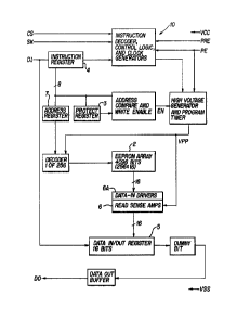
Figure 1 shows the basic elements of an electrically ~
erasable programmable read only memory (EEPROM) device. The ~`
device includes an EEPROM array 2 which is divided into 256 ;
storage registers of 16 bits each. N registers in the array can
be protected against data modification by programming into a ~ -~
special on-chip memory protect register 3 the address of the first
register in the array 2 to be protected. thereafter, all attempts `-,
to alter data in the storage register whose data address is equal ij ,
to or greater than the address stored in the memory protect -~
register 3 will be ignored. `
As shown generally in Figure 1, and described in greater ; ;~
detail below, data is written into a selected storage register ;
within EEPROM array 2 by serlally clocking a WRITE instruction
into instruction register 4 and then clocking 16 bits of data to -~ -
be written into the address specified in the WRITE ins~ruction
into data shift register 5. After the 16 bits of data have been
clocked into data shift register 5, this data is transferred in -
,,:
parallel to the specified storage register in array 2 via data in
drivers 6A in a single, self-timed WRITE cycle.
1332470
A READ instruction loads the address of the memory
register to be read from the instruction register 4
into an 8-bit address register 7. The data from the
accessed storage register is then transferred in
parallel to data shift register 5 via the sense
amplifiers 6 and then clocked out serially to the Data-
Out pin DO.
Fig. 2 shows serial read access circuitry 10 for
sequentially reading storage registers within array 2
in accordance with the present invention. The circuit
10 comprises two primary components: an address
register/counter 12 and a data stream counter 16.
The address register/counter 12 latches the
starting address input from the instruction shift
register 14 during plI.Io high. That is, when the
start bit of the instruction which is being serially
shifted into instruction shift register 14 migrates
over a series of clock cycles to register location IO,
the output plI.Io of AND gate 15 goes high, causing the
parallel transfer of the starting address from the
instruction shift register 14 to the address
register/counter 12. As will be described in greater
detail below, the address register/counter 12 has the
ability to count up in increments of ~ in response to
IAL pulse inputs to the address latch 12.
A data stream counter 16 monitors the number of
clock pulses during the READ mode and generates an
increment address latch (IAL) ~ignal at a fixed count.
The data stream counter 16 also generates a signal
RD.pl, during which time a new register in memory array
24 corresponding to the new incremented address in ,
address latch 12 is read by the sense amplifiers 22.
The new data is transferred into the masters and slaves
~` 1332~70
-7-
of the data shift registers 18 while the old data bit
D0 is clocked out of the dummy bit 26.
The data shift registers 18 are loaded either
6erially from the data-in (DI) pin 20 (as described
above in conjunction with a WRITE instruction) or can
be loaded in parallel during the RD.pl phase from the
sense amplifiers 22. As ~tated above, the data loaded
serially into the data shift register 18 is written
into the memory ~rray 24 in parallel. The data loaded -
in parallel to the 6hift registers 18 during a read
access is serially clocked out via dummy bit 26 and
data output drivers 28 onto the data output (D0) pad
30.
The mechanics of serial read access in accordance
with the present invention will be described with
reference to the timing diagram shown in Fiq.;2 and the
Fig. 1 ~chematic.
A read operation is accomplished by inputting a
READ instruction into the instruction register 14
through the data-in pin 20. The READ instruction
commences with a ~tart bit "1" followed by the op-code ;
and the address of the memory ~torage register to be
read. During the clocking sequence, while the last
address bit "Ao" $s latched into the ~Slave" at one end
of the instruction reglster 14 on the rising ~dge of
the pl clock, the ~tart bit is latched into the slave
of the instruction register 14 at the other end making
Io go high. In the illustrated embodiment, the Io
signal is delayed to provide an loPD signal which
provides enouqh time for all bits in the instruction
register 14 to stabilize. The IoPD 6ignal going high
forces the internal clock phases plI and p2I clocking
the instruction register 14 to 4top clocking. This
-8- 1 3 3 2 ~ 7 0
prevents any further da*a from being shifted into
instruction register 14.
As further shown in Fig. 2, the bits of data
stream counter 16 are initialized to zero when the READ
signal is low by resetting the flip-flops which
comprises the counter 16. With the IoPD signal goi~g
high, the READ instruction is decoded. The signal
RD.01 is true during the time READ and O1 are true and
the data 6tream counter 16 count is zero. During the ~i
time interval RD.01, the data from the register address
in array 24 specified in the READ instruction resident
in address register/counter 12 is latched into the data
shift register 18 and the dummy zero bit i6 output on
the data output pin 30 after a ~mall delay through the
data output driver. The dummy zero bit 6ignals that a
valid data ~tream is to follow. At the next clock
pulse p2, the data bits are shifted one position to the
right and at the following 01 clocX phase, the new data
bit (MSB of data, e.g. D15 in Fig. 3) is latched into
the slave portion of the last shift register (the dummy
bit). After some delay through the data output driver
28, the new data bit (e.g. D15) comes out on the data
output pin 30. In this way, for every successive input
clock phase, the next lower bit of data is output on
the data output pin 30.
~ ecause all the data bits (Dl5-DO in the
illustrated example) corresponding to a memory address
are latched into the data shift register 18 in parallel
when RD.pl is true, the address in the address latch
can be incremented while the data from the previous
~ddress is being ~erially clocked out on the data out
pin 30.
In the illustrated embodiment, a count of 7
(decimal) has been selected to generate a signal IAL
9 1332470
(increment address latch) to increment the address
register/counter 12 count by 1. Following the decoding
of the READ instruction, at the sixteenth clock phase
02, the data stream counter 16 rolls over to a count of
0 and during the sixteenth clock phase pl following the -~
READ decoding, the signal RD.pl is true again. During
the time interval when the RD.~1 signal is high, the -
data corresponding to the new incremented address is
transferred into the masters and slaves of all sixteen
data shift registers 1~. Simultaneously, the LSB (DO)
of the previous data stream is clocked out of the dummy
bit 26 into the data output drivers 28 and onto the
data output pad 30. On the seventeenth high going -;
phase of clock signal p2 following the decoding of the
READ instruction, the MSB (data bit D15*) of the
incremented address is shifted into the master of the
dummy bit and at the seventeenth high going phase of
01, the data bit DlS~ is output on the data output pad
30.
This sequence of events repeats for each 16 bits
of data. Thus, a continuous stream of data bits can
be serially clocked out of the data output pad 30
without the need for providing the new addresses to the
circuit 10 by inputting new ~EAD instructions over and
over again. This provides a substantial time savings.
In this way, the entire memory array 12 can be read in
one continuous data stream or as registers of length
varying from 16 to 4096 bits. Thus, the array 24 can
also be used as a shift register of variable lengths
(from 16 to 256 bits). `~
It should be understood that various alternatives
to the embodiment of the invention shown herein may be
employed in practicing the invention. It is intended
that the following claims define the invention and that
--1 o-- 1 3 3 2 4 7 0
circuits within the scope of these claims and their
equivalents be covered thereby.
,
.:
~1: , ''.':