Note: Descriptions are shown in the official language in which they were submitted.
-
1 ~3~84~
TWO WIRE LOW VOLTAGE DIMMER
Background Of The Invention
The present invention relates generally to a dimmer
circuit for controlling the RMS value of an AC voltage
applied to a load. In particular, the present invention
relates to a two wire dimmer circuit for use with reactive
loads where damaging DC load current may be present. The
present invention embodies correction means for decreasing
damaging DC current flowing through the load and voltage
compensating means for regulating the RMS value of the AC
voltage applied to the load. A two wire low voltage dim-
ming circuit without voltage compensating means but having
improved dimming ability at low load currents is also dis-
closed.
The present invention has particular application to
low voltage dimming systems wherein the load is a low
voltage transformer. However, the present invention also
has application to other types of loads, such as fluorsecent
lighting systems.
Two wire dimming circuits are known. One conven-
tional type of two wire dimming circuit comprises a triac
and a double phase shift firing circuit operatively connec-
ted to the triac's gate terminal. The double phase shift
firing circuit employs a series R-C circuit that is coupled
across the triac, and a firing capacitor coupled to the R-C
circuit by means of a potentiometer and to the gate terminal
of the triac by means of a diac. This circuit corrects
for damaging DC currents that are known to flow through
6232-3 CN *
-2- 1 3 3 2 8 4 4
reactive loads, such as the primary winding of a low voltage
transformer, by adjusting the firing angle of the triac in
selected half cycles of the waveform of the AC load voltage
in the following manner. The DC component appears across
the triac and hence also across what is known as the
"leading capacitor". The leading capacitor is the capa-
citor in the before referenced series R-C circuit. Since
the leading capacitor is connected to the firing capacitor
through the potentiometer, the DC voltage across the lead-
ing capacitor is added to the voltage across the firing
capacitor and the firing angle is altered to decrease the
DC current.
While the aforementioned two wire dimming circuit is
capable of solving the DC current problem that is known to
exist in reactive loads, it exhibits poor voltage regula-
tion. That is, it is not capable of maintaining the RMS
value of the AC voltage applied to the load substantially
constant with fluctuations in the AC supply voltage. It is
known to modify such a two wire dimmer so that it exhibits
good voltage regulation by replacing the leading capacitor
with a diac. The modified circuit, however, cannot correct
for the DC current problem once the leading capacitor has
been removed.
Three wire dimming circuits are also known. In a
three wire dimming circuit, two of the wires are connected
directly to the AC supply voltage and the firing angle is
determined from the voltage across the AC supply. Thus,
the firing angle is not affected by DC currents that may
flow through the load. It is known to those skilled in the
art to incorporate a voltage regulating diac in the three
wire dimmer's firing circuit. Such a three wire dimmer
exhibits good voltage regulation and does not exhibit the
DC current problem. Three wire dimmers, however, are
undesirable because three wires (AC hot, AC neutral and
load) must be run to each wall box, thus requiring addi-
tional installation cost.
1 332844
The present invention overcomes the failings of the
prior art by incorporating both a voltage regulation cir-
cuit and a DC current correction circuit in a two wire
dimmer.
Summary Of The Invention
A dimming circuit for use with reactive loads, such
as a low voltage transformer, comprises only a pair of
wires for connection in series with the load and an AC
supply voltage. First and second controllably conductive
thyristors are operatively coupled to the pair of wires
and a control circuit applies control signals to a gate
terminal of the first thyristor to fire the first thyristor
at a firing angle governed by the instantaneous magnitude
of the AC voltage appearing across the control circuit.
The second thyristor is rendered conductive only after
the load current through the first thyristor exceeds a
selected magnitude. The first thyristor is rendered non-
conductive after the second thyristor has been rendered
conductive. In the preferred embodiment the thyristors
used are triacs, but anti parallel connected SCR's or other
suitable devices could also be used.
A voltage compensating means is disposed in the
circuit for regulating the RMS value of the AC voltage
applied to the load. In the disclosed embodiment, the
voltage compensating means is a diac having a negative
resistance characteristic such that voltage applied to the
control circuit by the diac alters the timing of the con-
trol signals and hence the firing angle of the triacs when
fluctuations in the AC supply voltage occur, thereby main-
taining the RMS value of the AC voltage applied to the
load substantially constant. This compensating effect
occurs as long as the magnitude of the AC supply voltage
is greater than the breakover voltage of the diac.
The circuit also embodies correction means for cor-
recting asymmetries in the waveform of the AC load voltage
caused by DC current flowing through the load. A DC cur-
rent flowing through the load may cause advancing or
1 332844
--4--
retarding of the firing angle in positive or negative half
cycles of the waveform of the AC load voltage, depending
upon the magnitude and polarity of the DC current. Thus,
the waveform of the AC load voltage becomes asymmetrical.
The correction means corrects the asymmetries by advancing
or retarding the firing angle in succeeding half cycles
until the waveform of the AC load voltage is substantially
symmetrical, thereby decreasing damaging DC current flowing
through the load.
In the disclosed embodiment, the correction means
comprises a series combination of a resistor and correcting
capacitor coupled across the dimmer circuit. The correct-
ing capacitor charges to a voltage level that is indicative
of the magnitude and polarity of the DC current flowing
through the load. A feedback loop adds the voltage across
the correcting capacitor to the voltage across a firing
capacitor operatively coupled to the first triac's gate.
In each succeeding half cycle of the waveform of the AC
load voltage, the firing angle is advanced or retarded
(with respect to the firing angle in the preceding half
cycle of opposite polarity) by an amount governed by the
magnitude and polarity of the voltage across the correcting
capacitor.
In another embodiment, the correcting capacitor is
disposed in series with the voltage compensating diac.
The correcting capacitor is charged by the current flowing
through the voltage compensating diac to a voltage level
indicative of the magnitude and polarity of the DC current
flowing through the load. The voltage across the cor-
recting capacitor is applied in series with the diac to
effectively adjust the voltage being applied to the firing
capacitor, thereby advancing or retarding the firing angle
in each succeeding half cycle.
For the purpose of illustrating the invention, there
is shown in the drawings a form which is presently pre-
ferred; it being understood, however, that this invention
is not limited to the precise arrangements and instrumen-
talities shown.
1 332844
--5--
Brief Description Of The Drawings
Figure 1 is a block diagram of a known two wire low
voltage dimming circuit.
Figure 2 is a block diagram of a known three wire
low voltage dimming circuit.
Figure 3 is a schematic diagram of one embodiment of
a two wire low voltage dimming circuit according to the
present invention.
Figure 4 is a schematic diagram of another embodiment
of a two wire low voltage dimming circuit according to the
present invention.
Figure 5 is a schematic diagram of still another
embodiment of a two wire low voltage dimming circuit accord-
ing to the present invention.
Figure 6 is a schematic diagram of a prior art two
wire dimming circuit.
Figures 7, 8 and 9 are voltage waveforms illustrated
for use in describing the operation of the present invention.
Figure 10 is a schematic diagram of a known three
wire, dual triac dimming circuit.
Figure 11 is a schematic diagram of a two wire, low
voltage, dual triac dimming circuit without voltage compen-
sating circuitry according to the present invention.
Detailed Description Of The Preferred
Embodiment of the Invention
Referring now to the drawings wherein like numerals
represent like elements, there is illustrated in Figure 1 a
block diagram of a conventional two wire low voltage dim-
ming system labeled generally 10. Dimming system 10 com-
prises a two wire dimming circuit 12 having only a pair of
wires 26, 28 connected in series with the primary 20 of a
transformer 23 and an AC supply voltage 18. Dimming cir-
cuit 12 comprises a triac 16 having a control circuit 14
operatively coupled thereacross for supplying control
signals to the gate 17 for selectively rendering the triac
16 conductive. As is well known in the art, the timing of
the control signals and hence the firing angle of the
1 332844
--6--
triac governs the RMS value of the AC voltage applied to
the load. The dimmer circuit 12 illustrated in Figure 1
is shown as controlling the low voltage applied to a lamp
24 connected across secondary 22.
As is known, the firing angle of triac 16 is governed
by the instantaneous voltage across the control circuit
14, and hence across wires 26, 28. Thus, the firing angle
may be affected by the DC magnetizing current that flows
through the primary 20 of transformer 23. The magnitude
of this DC current may become significant and cause problems
hereinafter described.
The problematic DC current may be caused by a number
of factors. For example, if the lamp 24 or other load
connected across the secondary 22 of transformer 23 burns
out (i.e., becomes an open circuit), the magnitude of the
DC magnetizing current flowing through the primary 20 may
become significant compared to the RMS value of the AC
current flowing through the primary 20. Additionally, it
is conceivable that the supply of AC power to the circuit
10 could be momentarily interrupted at a time when the AC
voltage waveform is at or near zero after a positive or
negative half cycle. If, at the instant that AC power is
restored, the AC voltage waveform is again at or near
zero of a half cycle of the same polarity as was present
when power was removed, the magnetic material in the core
of transformer 23 may saturate and cause the transformer
to conduct current in one direction more easily than the
other. This delays the firing angle of triac 16 in one
half cycle of the AC voltage waveform (see Figure 9),
which causes the transformer 23 to polarize even more.
The regenerative nature of the phenomenon results in the
DC current problem.
Figure 2 illustrates a block diagram of a known
three wire low voltage dimming system 30. System 30 com-
prises a three wire dimmer circuit 32 having two wires 46,
48 coupled directly to the AC supply voltage 38. Wires
48, 50 are coupled to the primary 40 of a transformer 41
1 332844
for supplying a low voltage to a lamp 44 by means of secon-
dary winding 42. The dimming circuit 32 comprises a triac
36 and a control circuit 34 that supplies control signals
to the gate 37 of triac 36. Unlike the control circuit
14 of Figure 1, control circuit 34 is connected directly
across the AC supply voltage. Thus, the firing angle of
the control signals is not affected by any DC current that
may flow through the primary windings 40 of transformer 41.
However, the three wire dimming circuit of Figure 2 is not
only more expensive to manufacture than the two wire dimming
circuit of Figure 1, but three wire dimmers also require
that three, rather than two wires be run to a wall box
thus increasing the cost associated with the installation
of a three wire dimmer.
Figure 6 schematically illustrates a known two wire
dimming circuit 52. The circuit 52 illustrated in Figure
6 utilizes a type of control circuit for generating control
signals known as a double phase shift firing circuit. The
double phase shift firing circuit comprises resistor 54,
leading capacitor 56, potentiometer/trim circuit 58,
firing capacitor 60 and diac 62. The operation of this
circuit is well known in the art.
The two wire dimming circuit of Figure 6 does not
exhibit the previously discussed problems caused by DC cur-
rents flowing through the load if the characteristics of
triac 64 are selected according to certain criteria which
will be described later. If a DC component appears across
the triac 64, it also appears across the leading capacitor
56. Since the leading capacitor 56 is coupled to the
firing capacitor 60 through the potentiometer/trim circuit
58, the DC voltage across the leading capacitor 56 will
correct the firing angle of the triac 64 in selected half
cycles of the waveform of the AC load voltage. The effect
of altering the firing angle in this manner and an explana-
tion of how this corrects the DC current problem will
become evident hereinafter.
1 332844
--8--
While proper selection of the characteristics of
triac 64 will insure that the circuit of Figure 6 does not
exhibit the DC current problem hereinbefore described, it
does have another problem. The circuit of Figure 6 is not
capable of maintaining the RMS value of the AC voltage
applied to the load substantially constant with fluctua-
tions in the AC supply voltage. Such a voltage regulating
feature in a two wire DC compensating dimmer is desirable.
Prior attempts have been made to modify the clrcuit
of Figure 6 so that it performs the desired voltage regu-
lating function. One such modification involves replacing
the leading capacitor 56 with a diac so that the voltage
impressed upon the potentiometer/trim circuit 58 during
the period that the diac is in conduction varies in such a
manner as to modify the firing angle to compensate for
variation of the AC supply. This modification results in
a two wire dimmer that is voltage regulating as long as
the AC voltage does not fluctuate below the diac's break-
over voltage. But, the resulting dimmer is not capable of
correcting for DC current flowing through the load because
the modification necessitates the removal of the leading
capacitor 56. The following discussion explains why this
is so. In the following discussion, the term "modified
circuit" is used to refer to the circuit of Figure 6 that
is modified in the hereinbefore described manner by
replacing leading capacitor 56 with a diac.
Referring to the waveforms of Figure 7, 8 and 9 there
are illustrated relationships between AC supply voltage
(74, 74', 74''), AC load voltage (76, 76', 76''), AC load
current (78, 78', 78'') and AC voltage across the triac
(80, 80', 80''). As illustrated in each of the figures,
the AC load voltage (76, 76', 76'') is chopped by the
triac 64 in well known manner to supply a voltage of a
desired RMS value. As is also known in the art, adjust-
ment of the firing angle of triac 64 results in a cor-
responding adjustment of the RMS value of the AC voltage
applied to the load.
1 332~4
g
Figure 7 illustrates various waveforms of AC supply
voltage 74, AC load voltage 76 and AC load current 78 for a
purely resistive load that may be connected to the modified
circuit of Figure 6. As is seen, all of the waveforms are
substantially in phase and substantially symmetrical, in-
cluding the waveform 80 representing the AC voltage across
the triac 64. Thus, the operation of the circuit of Figure
6 when used with a purely resistive load is acceptable.
Figure 8 illustrates the same waveforms that result
when the modified circuit of Figure 6 is applied to a load
that is mostly resistive but has some inductive component.
As shown, the inductive component causes the AC current
waveform 78' to be slightly shifted out of phase with
respect to the AC load voltage waveform 76'. All of the
waveforms, however, are symmetrical. Thus, for the case
where the inductive component of the load is small, the
modified circuit of Figure 6 is also acceptable.
Figure 9 illustrates why the modified circuit of
Figure 6 is not acceptable for use in loads having both
a resistive component and a substantial inductive compo-
nent, such as a transformer load. Again, the phase of the
AC load current 78'' is slightly out of phase with respect
to the waveform 76'' of the AC load voltage. Saturation
of the magnetic materials in the load (transformer) may
cause the load to conduct current in one direction more
easily than in the other, thus causing the AC load current
78'' to increase to an abnormally high level, as shown at
84, during the time period that the AC load voltage 76''
is decreasing. Since the triac 64 is a current sensitive
device, it does not become nonconductive until the load
voltage 76'' has decreased enough to force the AC load
current 78'' below the holding current of the triac and
thus render the triac nonconductive as illustrated at "a"
in Figure 9. The net effect, as illustrated in Figure 9,
is that the DC current causes the firing angle of the
triac 64 to be shifted substantially during recurring
positive or negative half cycles, thus allowing the magni-
-
1 332844
--10--
tude of the AC load current to increase to abnormal levels.
Since this phenomenon occurs only during recurring positive
or negative half cycles, and not over the period of a full
cycle (compare tl to t2 in Figure 9), the waveform 76''
becomes asymmetrical.
As also illustrated in Figure 9, the shifting of the
firing angle during recurring half cycles causes the AC
voltage 80'' across the triac 64 to be greater in one half
cycle than in the preceeding half cycle of opposite
polarity. Further, the voltage across the triac 64 in the
positive half cycle can be seen to be lower than the voltage
during the negative half cycle. This means that the voltage
applied to the load is higher during positive half cycles
than negative half cycles, since the load voltage is equal
to the difference between the source and triac voltages,
and both half cycles of an AC source have essentially equal
RMS voltage values. Since the transformer primary to which
the load voltage is applied has a larger positive voltage
than it has negative voltage, it saturates in the direction
of positive current, which causes the peak current 84 to
increase its magnitude still further. Therefore, it can be
seen that a small asymmetry in the load voltage can, by its
influence on the dimmer conduction periods, give rise to a
positive feedback effect which results in a continuous
aggravation of what may have been a small initial distur-
bance until a much greater value of peak current 84 may
occur. It will be appreciated that if the peak magnitude
84 of the AC load current 78'' is permitted to increase
unchecked, a fuse may blow or a circuit breaker may open
or if temperatures rise to a sufficient level, a fire
hazard may exist.
The above discussion is for illustrative purposes
only and it will be appreciated that the DC current problem,
though described as occurring during positive half cycles,
could just as well occur during negative half cycles. In
any event, if the firing angle can be advanced or retarded,
as necessary, during the selected positive or negative
-11- 1 332~4
half cycles in which the DC current problem exists, the
potentially damaging DC current can be eliminated. Stated
otherwise, if the waveform of the AC voltage applied to
the load can be maintained symmetrical or caused to vary in
such a manner as to result in negative feedback instead of
the positive feedback described above, the hereinbefore
current problem will not occur. A dimming circuit for
achieving this function will now be described.
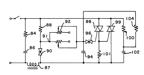
Referring to Figure 3, there is illustrated one em-
bodiment of a dimming circuit according to the present
invention. As in Figure 6, the dimming circuit of Figure
3 includes a RFI circuit comprising resistor 84, a capa-
citor 86 and an inductor 87. This RFI circuit does not
comprise a part of the present invention. The dimming
circuit also includes a control circuit comprising a
potentiometer/trim circuit 92, a diac 96 and firing capa-
citor 94 operatively coupled to the gate terminal of a
first triac 98 and to one terminal of potentiometer trim
circuit 92. A resistor 101 is in series with the triac 98,
and a second triac 99 connected across the dimming circuit
has its gate terminal coupled to the junction of the resis-
tor 101 and the first triac 98. The use of two triacs 98,
99, rather than a single triac, improves the operation of
the dimmer circuit at low load currents when the triacs are
selected in the manner hereinafter described.
The R-C series combination of resistor 88, poten-
tiometer/trim circuit 92 and capacitor 94 provide timed
control signals to the gate of triac 98. As is known, the
timing of the control signals (and hence the firing angle)
is at least partially governed by the setting of the
potentiometer in circuit 92. Additionally, the circuit
includes a voltage compensating means 90 for maintaining
the RMS value of the AC voltage applied to the load sub-
stantially constant, and correction means 100, 102 and 104
for correcting asymmetries in the waveform of the AC
voltage applied to the load to eliminate the DC current
problem previously discussed.
-12- 1 3 3 ~ 8 4 4
As shown, the voltage compensating means 90 comprises
a diac operatively coupled to the control circuit and in
particular to the other terminal 91 of potentiometer/trim
circuit 92 and to resistor 88. The diac 90 has a break-
over voltage that is applied to the control circuit, and
in particular to the potentiometer/trim circuit 92, when
the diac is in conduction. The control circuit is respon-
sive to the breakover voltage supplied by the diac 90 and
to fluctuations in the AC supply voltage to adjust the
timing of the control signals and hence the firing angle
of the triacs 98 and 99 to maintain the RMS value of the
AC voltage applied to the load substantially constant. As
in the modified circuit of Figure 6, this circuit will
regulate the AC load voltage as long as the AC supply
voltage does not fluctuate below the breakover voltage of
diac 90.
In the circuit of Figure 3, the correction means
comprises a series combination of a resistor 100 and a
correcting capacitor 102 coupled across the dimming cir-
cuit as shown. Correcting capacitor 102 charges to a
voltage level indicative of the magnitude and polarity of
the DC current flowing through the load. The voltage
across correcting capacitor 102 is coupled to the voltage
across firing capacitor 94 by means of feedback resistor
104. Thus, the voltage across firing capacitor 94 is
altered, thereby altering the firing angle of the triacs
98 and 99 in the next succeeding half cycle. The process
of feeding voltage back to the firing capacitor 94 con-
tinues for succeeding half cycles of the AC load voltage
waveform until the waveform has become substantially
symmetrical, i.e., until the DC current has been substan-
tially eliminated.
The dual triac configuration illustrated in Figure 3
overcomes several problems inherent in single triac type
dimming circuits. In single triac type dimming circuits,
the triac must be sized for maximum load current and hence
has a relatively high holding current. When the load cur-
1 332844
-13-
rent drops below the holding current, the triac drops out
of conduction and power is removed from the load. Thus, no
dimming can be performed for load currents that are below
the holding current. Moreover, the holding current for
forward and reverse directions of current flow through a
triac are not the same. This asymmetry may cause serious
problems in low voltage dimmers where the load has a sub-
stantial inductive component, such as in a low voltage
transformer, as it may be sufficient to activate the above-
described positive feedback mechanism which is inherent in
the operation of known two wire, low voltage dimmer cir-
cuits.
In the circuit of Figure 3, control signals are
applied to the gate of the first triac 98, as previously
mentioned. Thus, triac 98 becomes conductive when a con-
trol signal is applied to its gate and there is sufficient
voltage across the triac 98. Triac 99 is rendered conduc-
tive when the current through triac 98 and resistor 101
provides a voltage drop across resistor 101 sufficient to
fire triac 99. This voltage drop is nominally one volt
according to the preferred embodiment. When triac 99 is
fully conductive, the voltage between the anode and gate
of triac 99 is essentially zero and triac 98 no longer
has significant current flowing therethrough. When the
current through triac 98 drops below the holding current,
triac 98 turns off and triac 99 carries the full load
current of the dimming circuit.
If the load current through triac 98 is low enough,
the voltage drop across resistor 101 will not be great
enough to trigger triac 99 into conduction in the manner
described above. In this case, triac 98 will not, as
before, be turned off by triac 99, but instead will carry
full load current until the load current becomes great
enough to trigger triac 99 into conduction.
The advantage of utilizing two triacs, as described
above, lies in the ability to select the characteristics of
triacs 98 and 99 independently for both low and high ranges
` 1332844
-14-
of load current. Another advantage lies in the ability to
define the boundary between those operating ranges by
selecting an appropriate value for resistor 101. The
primary factor that determines the characteristics of triac
99 is the maximum load current rating of the dimming
circuit, i.e., triac 99 must be able to conduct the maximum
load current reliably. Another characteristic that must
be chosen is each triac's holding current. Triac holding
current varies greatly among different specimens of the
same type of triac, and also with temperature and current
rating. The following summarizes the considerations that
must be taken into account when selecting the triacs for
use in the circuit of Figure 3.
The most problematic operating condition of a two
wire low voltage dimmer operating a transformer load occurs
when the transformer is unloaded. Under this condition,
the current through the conducting triac (typically the
triac 98 in Figure 3) is very low and, for each half cycle
of AC load current, may be only slightly greater than the
holding current. In such case, when the load current
begins to decrease, as it does toward the end of each half
cycle, the triac can drop out of conduction before the zero
crossing of the AC load voltage. The angle at which the
triac drops out of conduction may be significantly dif-
ferent in positive and negative half cycles, due to the
beforementioned asymmetry of holding current. The result
of this differing conduction, in each half cycle, is that
the transformer sees a DC voltage component and may be
driven into saturation as a result.
The holding current of a triac is generally on the
order of 1/1000 of its maximum current rating. Therefore,
a 25 amp rated triac, for example, would be expected to
have a holding current of about 25 mA. Even this rela-
tively low holding current can cause serious transformer
saturation problems because the peak magnetizing current
of a small low voltage transformer may be on the order of
only 40 or 50 mA. If one could use a 0.8 amp rated triac,
1 332~44
-15-
the holding current would be on the order of 0.8 mA, which
is relatively insignificant compared to the magnetizing
current. However, a 0.8 amp triac cannot sustain the
desired full load current or transient surges that are
common in dimmer applications.
Referring to Figure 3, if the value of resistor 101
is chosen at approximately 5 ohms, only triac 98 will
conduct if the peak load current is less than about 200
mA, i.e., 200 mA is required to provide a 1 volt drop
across a 5 ohm resistor and thereby render triac 99 con-
ductive. Thus, triac 98 can be rated for a relatively low
maximum load current, thereby providing a very low holding
current, as hereinbefore described. If the load current
increases above 200 mA, triac 99 will turn on and triac 98
will turn off, as above described. Triac 99 will handle
the full load current, and its relatively higher holding
current will be unimportant at these higher load currents.
The above example where triac 98 is rated at 0.8 amps
and triac 99 is rated at 25 amps, is a typical ratio. The
value chosen for resistor 101 depends on the actual current
ratings, but generally should be chosen to give a one volt
drop at a current level of about 1/10 to 1/2 of the max-
imum current rating of triac 98. This insures that low
load currents are conducted only through triac 98 and that
only high load currents are conducted through triac 99.
Figure 4 illustrates another circuit embodiment
according to the present invention. Again, a RFI circuit
comprises a resistor 106, a capacitor 108 and an inductor
116. A control circuit for supplying control signals to
the gate terminal of a first triac 124 comprises resistor
110, potentiometer/trim circuit 118, diac 120 and firing
capacitor 122. As before, a resistor 127 is in series with
a first triac 124. A second triac 125 is connected across
the dimming circuit and has its gate terminal coupled to
the junction of resistor 127 and triac 124. Triacs 124
and 125 are selected in the same manner as triacs 98 and
99 hereinbefore described.
--- 1 3 3 2 8 4 4
-16-
A diac 112 is coupled to the control circuit, and
particularly to the potentiometer/trim circuit 118, as
shown. A correcting capacitor 114 is connected between
the diac 112 and one side of the dimmer circuit in the
manner shown. A resistor 113 couples the other side of
the dimmer circuit to the junction of diac 112 and correct-
ing capacitor 114. As before, diac 112 supplies a com-
pensated breakover voltage to the control circuit, and
particularly to potentiometer/trim circuit 118 when the
diac is in conduction. The control circuit is responsive
to fluctuations in the AC supply voltage and to the break-
over voltage to adjust the firing angle of the control
signals and maintain the RMS value of the AC voltage
applied to the load substantially constant. As before,
the RMS value of the AC voltage applied to the load will
remain substantially constant as long as the AC voltage
does not fluctuate below the breakover voltage of the
diac. Thus, in the circuit of Figure 4, diac 112 performs
the voltage regulating function.
In the circuit of Figure 4, the correcting means
comprises capacitor 114, resistor 110, diac 112 and
resistor 113. The current through resistor 110, diac 112
and resistor 113 charges capacitor 114 to a voltage level
that is indicative of the magnitude and polarity of the DC
current flowing through the load. The voltage across
correcting capacitor 114 is applied in series with the
diac 112, thereby effectively adjusting the voltage applied
to the firing capacitor 122 through the potentiometer/trim
circuit 118. This variation in voltage applied to firing
capacitor 122 through potentiometer/triac circuit 118
will correct the firing angle in each succeeding half
cycle, thereby removing any asymmetries in the AC voltage
waveform and thus substantially eliminating the DC current.
The value of the correcting capacitor 102 utilized in
the circuit of Figure 3, and the value of the capacitor 114
utilized in the circuit of Figure 4 must be large enough
so that there is only a relatively small AC impedance.
1 332~44
-17-
Preferably, the correcting capacitors 102, 114 should be
sized so that they represent a substantial short circuit
to AC current. Thus, only a small ripple voltage should
appear across the correcting capacitors 102, 114.
The embodiment of Figure 5 is substantially identical
to the embodiment of Figure 4, except that the circuit of
Figure 5 utilizes two electrolytic capacitors 138, 140 and
two diodes 134, 136 to replace the capacitor 142. This
modification minimizes the physical size of the circuit and
allows installation in a standard wall box. Again, the
previous discussion of how the triacs are selected is
applicable.
According to another aspect of the invention, there
is provided a two wire low voltage dimming circuit without
voltage compensating means but having improved dimming
ability at low load currents and improved resistance to the
DC current problem hereinbefore described. Such circuit
incorporates dual triacs selected according to the criteria
previously discussed.
Figure 10 illustrates a known three wire dimming cir-
cuit having three wires 160, 162, 164 for connection to an
AC supply 146 and a load 152. As shown, load 152 is a low
voltage transformer comprising a primary 154 and a secondary
156 coupled to an incandescent lamp 158. Circuit 142 com-
prises dual triacs 148, 150 and a resistor 151 in series
with triac 148, as shown. The gate of triac 148 receives
control signals from a control circuit 144. The gate of
triac 150 is operatively coupled to the junction of resis-
tor 151 and triac 148. It is known, in connection with the
construction of the three wire dimmer circuit 142, to select
triacs 148, 150 according to the criteria previously dis-
cussed. As has been mentioned, however, three wire dimmer
circuits of the type illustrated in Figure 10 are undesirable
because three wires must be run to each wall box, thereby
increasing installation costs.
According to the present invention, there is provided
a two wire low voltage dimming circuit utilizing dual triacs
1 332844
-18-
selected according to the criteria discussed herein. Such
a circuit is illustrated in Figure 11 and labelled generally
166. Circuit 166 is DC correcting but is not capable of
voltage regulation for the same reasons as described in con-
nection with the circuit 52 illustrated in Figure 6. Circuit
166 comprises only a pair of wires 172, 174 for connection
in series with an AC supply and a load. As before, the load
may be a low voltage transformer. Also, the circuit 166,
with minor modification, may be used as a fluorescent light
dimmer and connected in series with a ballast.
As before, circuit 166 includes a RFI filter comprising
a capacitor 168, resistor 170 and inductor 176, connected
as shown. The RFI filter does not comprise any part of the
present invention. Circuit 166 also includes a series R-C
circuit combination, i.e., resistor 170 and capacitor 178,
operatively coupled across the pair of wires 172, 174
through inductor 176. The junction of resistor 170 and
capacitor 178 is operatively coupled to one side 179 of a
potentiometer/trim circuit 180. The other side 181 of
potentiometer/trim circuit 180 is operatively coupled to a
diac 184 in series with the gate of triac 186. A capacitor
182 is operatively coupled across the potentiometer/trim
circuit 180 and the junction of capacitor 178 and inductor
176, as shown. Triac 186 is operatively coupled in series
with a resistor 188 across the pair of wires 172, 174
through inductor 176. Triac 190 is operatively coupled
directly across the pair of wires 172, 174 through inductor
176 as shown and its gate terminal is operatively coupled
to the junction of resistor 188 and triac 186. Triacs
186, 190 are preferably selected in the manner hereinbefore
described and their operation is also as previously des-
cribed.
The circuit of Figure 11 is DC correcting but does
not perform voltage regulation. However, the circuit of
Figure 11 exhibits improved dimming ability at low load
currents for the reasons previously described. Still
further, the dual triacs used in the circuit of Figure 11
1 332844
--19--
prevent the problems that are normally caused where the
load has a substantial inductive component.
The present invention may be embodied in other speci-
fic forms without departing from the spirit or essential
attributes thereof and, accordingly, reference should be
made to the appended claims, rather than to the foregoing
specification, as indicating the scope of the invention.