Note: Descriptions are shown in the official language in which they were submitted.
1332883
RECTILINEARLY DEFLECTABLE ELEMENT
FABRICATED FROM A SINGLE WAFER
Backqround
5The present invention relates to deflectable
elements which are suitable for use, with appropriate
electronics, as either force transducers or actuators.
It is known to fabricate force transducers from
silicon substrates by etching suspended beams, or similar
.10 structures, which deflect in response to the application
of a force to be measured. The deflection may be
electronically measured by conventional means such as
resistive strain gauges or piezoelectric elements.
Typical applications of these force transducers include
accelerometers, pressure sensors, gravity sensors, and
microphones.
A difficulty encountered with many known devices
is that internal bending moments of the suspended
structure are cancelled by reactions at the fixed
boundary which prohibit flexure with simultaneous
-boundary displacement. Stated another way, these devices
typically have not provided rectilinear displacement of
the suspended structure Accordingly, a nonlinearity has
been introduced into the electrical representation of the
applied force. Another problem is that the amount of
flexure is limited by the amount of bending a given
dimension of a silicon structure is able to withstand
before fracturing.
A prior approach to provide rectilinear
displacement of a suspended element is disclosed in U.S.
patent 4,071,838. More specifically, a structure is
disclosed which may be characterized as a pair of
opposing E-shaped springs joined together at their arm
extremities and fabricated from a single monocrystalline
wafer. The resulting center arm allegedly deflects in a
~k`
133~883
rectilinear relationship to the applied force. A
disadvantage of this approach is the complexity of the
structure and associated complexity in fabricating.
Another disadvantage is that the range of rectilinear
displacement is limited by the amount of bending the
silicon segments are able to withstand before fracturing.
In another approach, U.S. patent 4,144,516
discloses a multiple wafer structure, each wafer having a
pair of opposing E-shaped springes. The two wafers are
bonded together to extend the range of rectilinear
deflection of the E-shaped springs. A disadvantage of
this approach is the added complexity of the two wafer
design.
Summary of the Invention
In one aspect of the invention, there is provided a
method for forming a suspended element from a tlO0]
silicon substrate wherein movement of the suspended
element is rectilinear and proportional to an external
force, comprising the steps of:
etching two cavities in said substrate thereby
defining a centre member between said cavities having a
first planar face and an opposing second planar face,
said cavities also defining a supporting frame connected
to opposing ends of said centre member;
forming a passivation layer on said first planar
face with a pair of passivation openings symmetrically
positioned on said first planar face for anisotropic
etching in a subsequent step, each of said passivation
openings having dimensions such that the set of [111]
planes adjacent said passivation opening define a point
of convergence beyond said silicon substrate;
applying an anisotropic etching to said passivation
openings for forming a pair of recesses in said centre
member thereby defining said suspended element; and
timing said step of anisotropic etching such that
each of said pair of r~cecs~s forms a narrowed portion of
_ 3 _ 13~ 2 88 3
said centre member between said second planar surface and
each of said recesses, said narrowed portions defining a
pair of flexing members for providing rectilinear
deflection of said suspended element in linear proportion
to the applied force.
In a further aspect of the invention, there is
provided a method for forming a suspended element from a
[100] silicon substrate wherein movement of the suspended
element is rectilinear and proportional to an external
force, comprising the steps of:
etching two cavities in said substrate thereby
defining a centre member between said cavities having a
first planar face and an opposing second planar face,
said cavities also defining a supporting frame connected
to opposing ends of said centre member;
forming a passivation layer on said first planar
face having a first pair of passivation openings
symmetrically positioned on said first planar surface and
forming a passivation layer on said second planar surface
having a second pair of passivation openings
symmetrically positioned on said second planar surface
and offset from said first pair of passivation openings,
each of said passivation openings having dimensions such
that the set of [111] planes adjacent each of said
passivation opening define a point of convergence within
said silicon substrate;
applying an anisotropic etchant to said passivation
openings for forming a first pair of recesses through
said first planar surface and a second pair of recesses
through said second planar surface wherein said suspended
element is defined as the portion of said centre member
between said first pair of recesses; and
timing said step of anisotropic etching to form a
narrowed portion of said centre member between each of
said first pair of rec~ses and each of said second pair
of recesses, said narrowed portions defining a pair of
flexing members for providing rectilinear deflection of
13~2883
- 3A -
said suspended element in linear proportion to the
applied force.
In accordance with the aspects of the invention
described above, an advantage is obtained of providing a
greater range of rectilinear movement from a single
substrate than heretofore possible. further, the range
of deflection may be increased by simply etching
additional flexible members. Since the recesses may be
etched to the same depth, they all may be fabricated in
one step thereby obtaining another advantage.
Brief description of the Drawin~s
The objects and advantages described herein
will be more fully understood by reading the Description
of the Preferred Embodiment with reference to the
drawings wherein:
Figure 1 is a perspective view of an embodiment
in which the invention is used to advantage;
Figure 2 is a cross-sectional view taken along
_ 4 _ 13 3 2 8 8 3
line 2-2 of Figure l;
Figures 3A-3C illustrate sequential fabrication
steps for fabricating the embodiment shown in Figure l;
Figure 4 is a cross-sectional view of an
alternate embodiment in which the invention is used to
advantage;
Figure 5 is a cross-sectional view of another
alternate embodiment in which the invention is used to
advantage;
Figure 6 is a perspective view of still another
alternate embodiment in which the invention is used to
advantage;
Figure 7 is a cross-sectional view taken along
line 7-7 of Figure 6; and
Figure 8 illustrates a modification of the
embodiment shown in Figures 6 and 7 for use as a pressure
transducer.
DescriPtion of the Preferred Embodiment
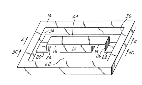
In general terms, with reference to Figure 1,
suspended element 12 is shown integrally connected to
supporting frame 14 by flexible members 16, 18, 20, 22,
24 and 26. Suspended element 12, frame 14, and each of
the flexible members are fabricated from a single wafer
or substrate 28 (Figure 3A) as described in greater
detail hereinafter with particular reference to Figures
3A through 3C.
Continuing with Figure 1, and also referring to
Figure 2, flexible member 16 and nearly identical
flexible member 18 define a pair of flexible members
shown connected to respective opposing outer ends 30 and
32 of suspended element 12 forming respective angles A
and B therebetween. Similarly, flexible member 20 and
nearly identical flexible member 22 define another pair
of flexible members connected to respective opposing
133~8Y3
inner ends 34 and 36 of frame 14 forming respective
angles C and D therebetween. Flexible member 24 is shown
interconnecting flexible members 16 and 20 thereby
forming respective alternate angles E and F. Similarly,
flexible member 26 is shown interconnecting flexible
members 18 and 22 thereby forming respective alternate
angles G and H.
The symmetrical positioning, with respect to
suspended element 12, of each flexible member of a
respective flexible member pair provides rectilinear
movement in response to a force applied against suspended
element 12. For example, in the event that a force such
as an inertial force deflects suspended element 12 in an
upward direction, the bending moments at each boundary of
the flexible member causes: angles A and B to decrease by
the same degree; angles E and G to increase by the same
degree; angles F and H to increase by the same degree;
and angles C and D to decrease by the same degree.
Accordingly, the boundary between suspended element 12
and flexible member 16 is displaced directly upward; the
boundary between flexible members 16 and 24 is displaced
upward and toward suspended element 12; and the boundary
between flexible members 24 and 20 is displaced upward
and away from the suspended element 12. Likewise, the
boundaries between suspended element 12, flexible member
18, flexible member 26, and flexible member 22 are
displaced in the same manner. This symmetrical movement
of the flexible members permits rectilinear deflection of
suspended element 12. Further, by the use of appropriate
flexible member materials, such as silicon, wherein any
strain in the flexible members caused by an applied
stress is within their linear range, the deflection of
suspended element 12 is in direct linear proportion to
the applied force.
Referring to Figures 3A through 3C, wherein like
1332883
-- 6 --
numerals refer to like parts shown in Figures 1 and 2,
the fabrication of suspended element 12, support frame
14, and flexible members 16, 18, 20, 22, 24 and 26 is now
described. The fabrication described herein utilizes
photolithographic and etching techniques well-known in
the microelectronics industry. Substrate 28 is
illustrated in Figure 3A as a silicon wafer, preferably
having a thickness of approximately 200 to 500 microns,
with major surfaces lying substantially in the {110}
plane. Top and bottom silicon oxide layers 38 and 40,
respectively, are grown on substrate 28 using
conventional techniques well known in the semi-conductor
industry. Layer of silicon nitride 42 and layer of
silicon nitride 44 are the deposited over respective
silicon oxide layers 38 and 40, respectively, using
conventional vapor deposition techniques. Layer of
silicon oxide 38 and layer of silicon nitride 42 form a
conventional passivation layer 43. Similarly, layer of
silicon oxide 40 and layer of silicon nitride 44 form
passivation layer 45.
Referring now Figure 3B, center member 60 and
frame 14 are formed by etching a pair of openings or
cavities 62 and 64 (Fig~re 1) through substrate 28 by use
of well-known photolithographic technology and wet
etching with an anisotropic etchant solution, such as
aqueous potassium hydroxide solution or ethylene diamine
pyrocatechol solutions. It is to be understood that dry
etching techniques utilizing a gas may also be used, but
the intrinsically slower etch rates may be useful only in
thin materials.
Photo resist layers 46 and 48 are deposited over
respective passivations layers 43 and 45, and passivation
openings 50, 52, 54 and 56 are delineated utilizing
conventional photolithographic techniques. Passivation
openings 50, 52, 54 and 56 are extended through the
1332883
-- 7
passivation layers 43 and 45 to expose respective
portions of surfaces 70 and 78 of center member 60 as
shown in Fig. 3B. Thus, passivation openings 50, 52, 54
and 56 form conventional mask openings for subsequent
etching of center member 60.
A wet anisotropic etchant, such as described
hereinabove, is applied to etch the exposed portions of
surfaces 70 and 78 of center member 60 such that
respective recesses 66 and 68 are formed in surface 70
extending from passivation openings 50 and 52; and,
respective recesses 74 and 76 are formed in surface 78
extending from passivation openings 54 and 56 as shown in
Fig. 3C. Etching of the {110} plane is timed such
that flexible members 16, 18, 20 and 22 have a thickness,
and accordingly the related flexibility or spring
constant desired.
Since the anisotropic etchant acts against the
- {110} planes at a rate approximately 100 times
greater than the etchant acts against the lateral
{111} planes, the final shape of the etched areas is
determined by the slowly etched {111} surfaces and
the remaining unetched {110} surfaces which bound the
etched volume. Thus, fQr the illustrated {110}
wafer, recesses 66, 68, 74 and 76 each define a
substantially rectangular recess extending inwardly from
the passivation openings.
The spacing between the recesses 66 and 74, as
determined by the offset between passivation openings 50
and 54, substantially defines the thickness of flexible
member 24. Similarly, the spacing between recesses 68
and 76, as substantially determined by the offset between
passivation openings 52 and 56, defines the thickness of
flexible member 26.
Figure 3C illustrates the resulting structure
after the photo resist material has been removed. For
1332883
-- 8
clarity in illustration, passivation layers 43 and 45 are
not shown in Figure 3C.
Those skilled in the art will recognize that
different crystaline structures will result in recesses
of different shapes. For example, a {100} crystaline
structure results in the recesses as described later
herein with particular reference to Figures 4 and 5. It
should also be noted that the formation of multiple
flexible members, as described herein, provides the
advantage of requiring only a single etching step from a
single substrate.
Referring now to Figures 4 and 5, wherein like
numerals relate to like parts shown in Figures 1 and 2,
wet etching in {100} wafers of silicon is shown. In
a {100} crystaline structure, the lateral {111}
planes intersect the normal {100} plane at an angle
of 54.7. An anisotropic etchant, as described
hereinabove, acts against the {100} planes at a rate
approximately 100 times greater than the {111}
planesN Accordingly, the etchant acts against the
{100} planes leaving etched volumes bounded by the
{111} planes.
For the embodi~ent shown in Figure 4, the
etchant step is timed such that the etching against the
{100} planes defines the thickness of flexible
members 16', 18', 20' and 22'. Flexible members 24' and
26', however, have a thickness essentially determined by
the positioning of the passivation openings (not shown)
with respect to one another. That is, since the etchant
acts against the {111} planes at a rate approximately
only l~lOOth the {100} planes, the spacing of those
{111} planes extending from the opposing passivation
openings essentially determines the thickness of flexible
members 24' and 26'. It is to be noted, however, that
some etching against the {111} planes will occur
1332883
g
dependent upon the etching time. Accordingly, the
thickness of flexible members 24' and 26' is not
perfectly defined by the spacing of the passivation
openings with respect to one another.
Although the photo resist openings are not shown
in Figure 4, it is apparent to one skilled in the art
that they may be defined as the intersection of recesses
66' and 68' with surface 70', and recesses 74' and 76'
with surface 78'.
Referring now to the embodiment shown in Figure
5, wherein another {100} silicon substrate is
illustrated, it is seen that the {111} planes
defining the outer walls of recesses 66'', 68'', 74'' and
76'' intersect or converge within the silicon substrate.
That is, the {111} planes extending from the
perimeter of each passivation opening (not shown)
intersect within the silicon substrate. Since the
anisotropic etchant etches against the {100} plane at
a rate approximately 100 times greater than the {111}
planes, the anisotropic etchant etches against the
{100} plane to the intersection of the {111}
planes as illustrated in Fig. 5. At the intersecting
point the etch rate dro~s drastically giving the operator
more than sufficient time to remove the wafer from the
etchant and wash the wafer clean of etchant chemicals.
It is to be noted that extending the perimeter
of the passivation openings (not shown) such that the
{111} planes extending therefrom would converge off
the substrate, would result in a structure similar to
that shown in Figure 4; provided, however, that the
etching time is controlled to prevent etching of the
{100} plane through the substrate. Accordingly, an
advantage provided by the embodiment shown in Figure 5 is
that the etching time does not require strict control.
As previously described with respect to the
1332883
-- 10 --
embodiment shown in Figure 1, another advantage obtained
by the embodiments shown in both Figures 4 and 5 is that
multiple flexible members are obtained on a single
substrate by a single etching step.
Another alternate embodiment is now described
with particular reference to Figures 6 and 7. Suspended
element 110 is here shown suspended between cavities 106
and 108. Support frame 116 and suspended element 110 are
integrally connected by a single pair of symmetrical
flexible members comprising flexible member 118 and
flexible member 120. Angle T is defined as the angle
between flexible member 118 and outer end 122 of
suspended element 110. Similarly, angle U is defined as
the angle between flexible member 120 and outer end 124
of suspended element 110. The angle between flexible
member 118 and inner end 128 of frame 116 defines angle
V. Similarly, angle W is defined as the angle between
flexible member 120 and inner end 126 of frame 116.
Deflection of suspended element 110 is
restrained to be rectilinear by the symmetrical bending
of flexible members 118 and 120. In response to an
upwardly applied force, for example, localized bending
moments at a bending axis near the boundary between
flexible members 118 and outer end 122 result in a
2S reduction of angle T. As a result of the symmetrical
positioning of flexible members 118 and 120, angle U is
concurrently reduced by the same degree as angle T. In a
similar manner, angles V and W are increased by the same
degree. Accordingly, suspended element 110 moves in a
rectilinear direction in response to an applied force.
Since the structure illustrated in Figures 5 and 6 is
constructed of a material wherein strain is a linear
function of applied stress, herein shown as silicon, the
deflection of suspended element 110 is also linearly
proportional to the applied force.
- 11- 1332883
Another alternate embodiment is shown in Figure
8 wherein the structure depicted in Figures 6 and 7 is
adapted for use as a pressure sensor. Referring to
Figure 8, wherein like numerals refer to like parts shown
in Figures 6 and 7, the silicon wafer is doped to be a
p-type semiconductor by conventional diffusion of an
impurity such as boron into the silicon wafer. A layer
of silicon oxide is grown by the use of well-known
techniques over the top of wafer 128'. Accordingly,
after the underside etching of cavities 106' and 108'
(Figure 7), and of recesses 112' and 114', a seal of
silicon oxide will remain for preventing the flow of a
fluid through cavities 106' and 108'.
Silicon wafer 128' is shown bonded to an
insulating substrate such as glass substrate 134. An
insulating layer 136, preferably silicon 02ide grown on
the bottom side of wafer 128', is shown positioned
between wafer 128' and glass substrate 134. Metal plate
138, preferably of aluminum, is shown deposited on glass
substrate 134 below suspended element 110 to form one
electrode of a plate capacitor as described hereinbelow.
Metal contact 140, preferably aluminum, is shown
extending through substrate 134 for providing an external
electrical contact to metal plate 138. Similarly, metal
contact 142 is shown extending through glass substrate
134 for contacting with wafer contact 144, shown coupled
to wafer 128' in a conventional manner.
As shown in Figure 8, suspended element 110 and
metal plate 138 form two plates of a capacitor having an
air dielectric 146 therebetween. Accordingly, in
response to a change in pressure against suspended
element 110, a corresponding change in capacitance is
detected by conventional electronic circuitry (not shown)
across contacts 140 and 142. Since suspended element 110
is rectilinearly deflected and the amount of deflection
1332883
- 12 -
is linearly proportional to the applied pressure, the
change in capacitance is linearly proportional to the
applied pressure. Accordingly, a very linear measurement
of pressure is obtained.
Although fabrication has been illustrated using
silicon in the embodiments shown hereinabove, those
skilled in the art will recognize that numerous other
substrates may be used to advantage. A silicon
substrate, however, may be advantageous to use in
applications wherein electronic circuitry is fabricated
on the same silicon substrate using techniques well known
in the microelectronics industry. Further, the silicon
may be doped to carry electrical current thereby
minimizing the need for e~ternal electronic circuitry.
This concludes the description of the preferred
embodiment. The reading of it by those skilled in the
art will bring to mind many alterations and modifications
without departing from the spirit and scope of the
invention. Accordingly, it is intended that the scope of
the invention be limited only by the following claims.