Note: Descriptions are shown in the official language in which they were submitted.
1332958
CONTROL SWITCH
~ACKGROUND OF THF INVENTION
5~ Ficld o~ the Invention
S The present invention generally relates to control switchcs, snd more
4 particularly to a device intcnded for use as a light dimmer switch.
PescriDtjor. of the Prior Art
Power switches are manufactured in all shapcs and sizcs for a sundry of
7 diffcrent purposes. The prcsent application is directed to a particular powcr
8 switch which, although intcndcd for use as a light dimmer, could bc uscd
9 with motors and in othcr applicstions. Electrical switch~ of the type rcferrcd
to hcrein generally consist of two or morc wires for connection to an cxtcrnal
11 power source, a pair of metal contacts connectcd to thesc wircs, ant a lever
12 or button uscd to actuatc thc contacts betwecn open and closed states.
There are several diffcrent types of light switches. Thcsc include knifc
14 switches, mercury switches, turnstile type switchcs, tumblcr switchcs, push~
~5 button switches and clectromagnctic switchcs, all familiar to thosc skillcd in
1~ the art. A network of lights may bc managed by a singlc rOtary powcr
17 switch having a plurality of contscts. For light dimming circuits, early
18 switches incorporated a rheostat or potentiometcr for rcgulating the power
19 transmitted to thc light bulb. Modern dimmers use a triac firing circuit
which gcnerates considerably IC8S heat and power loss than the older poten-
a1 tiometer configuration, although a variable resistor is still employet to adjust
82 the firing ran~e of the trisc.
2~ Scveral problcms arisc in the manufacture, installation, and use of dimmer
24 switches. Onc such problem occurs in slide-type dimmers. l hC sllae ~no~
2~S cxtcnds outward from the intcrnal mechsnisms ~of the switch, leaving an
~2~ unsightly 8aP which peers inside thc devicc. Also, a rclativcly cxpensive
:~7 bearing system must be provided to insure smooth movement of the slide
28 1¦ along its path. These difficulties are encountered in the fabrication
*
13329S8
of thc switch which is fastcncd to a surrounding box on the backsidc of thc
switch. The rnoving parts of the switch, as well as thc circuitry, cannot be
tested until thc back bo~ is in place, thereby sccuring 811 of thc mcchanical
4 and clectricsl componcnts togethcr. If, howcver, a particular unit should fail
the tèst performcd just befo-e packing, thcn thc entirc unit must be disas-
~, sembled (i.e., the box and strap removcd), in order to dcterminc the causc o~
7 the failure. If this problcm arises frcquently in a mass production setting, it
8 rcsults in a substantial increase in labor costs during manufacturc
9 The ne~t complication occurs during installation of thc switch. With
scveral types of switches, it is impossible to tell whcther thc switch is in an
11 ~on" or ~off" statc. ThiQ creatcs a safety hazard during insta11ation sincc an
12 clectrician or homeowner may install a switch which is closcd, e~cposing thc
1~ person to a livc circuit. Even if the switch i8 markcd as to on and off
14 positions, thc installer may not notice what state thc switch is in during1~ installation. At the prcscnt time, there arc no safcty featurcs sssociated
1~ with the switchcs thcmselvcs which would overcome this problem.
17 Thc final difficulty concerns findin8 thc light switch whcn the room is
18 complctcly dark. Several switches havc becn manufactured which overcomc
1~ this problcm by actually placing a small bulb within thc device, for e~smplc,
ao within a transluccnt lever srm which actuates the switch Thc main disad-
21 vanta8e to this type of switch, however, is that the bulb cvcntually burns out.
22 I It would, therefore, be desirablc and advantageous to devise a light
25 I dimming switch which would overcome the abovc-stated problems. The present
a~ ~ invention does so by providing I ) a novel slidc arrsngcment having ~n ultra-
SS~ thin profile, 2) a switch framc which holds the cQmponents together without
8~ attachment of the back bo~, 3) a unique air gap lever which prevents premature
a7 actuation of thc switch~ and 4) a novel light pipe which doubles as an actuator
88 arm for full on-off.
29
SUMMARY OF THE INVFNTIQN
51 1 Accordingly, the primary object of the prcscnt invent;on is to providc a
52 I control switch for dimmin8 lighting fi~tures.
1332958 ~: ~
1 Another object 0r the invention is to providc such a switcb with a slid;ng
51 hsndlc or knob hsving a slim profile and smooth opcration.
Still another object of thc invention is to provide a switch framc whercby
4 all components of the switch may be held intact without final asscmbly of
t~ the switch, thcreby simplifying correction Or defects if the device fails final
d testing.
7 Yet another object of thc invcntion is to provide a safcty featurc
8 preventing accidental shock during installation or changc-out of a lsmp.
8 A further object of the invention is to providc such a switch having an
illuminated on-off button which is cost-effcctive and durable .
.1 The foregoing objects are achieved in a control switch having a novel
12 slide arrangement, frame, air ~ap lever, and light piping. Thc slide arrangement
13 . compriscs a slide base interposed between a slidc clip and slide knob, the
1~. slide clip having pairs of indented dimplcs which ride rails on the slidc basc.
1~5 The frame surrounds the slide arrangemcnt and has sevcral clip srms which
1~ extend downward through the switch strap, and clip onto the printed circuit
17 board containing the electric~l components of thc switch. ~he air gap Icvcr
18 is positioned on the front side of the switch and coupled to a butt contact :.
1~ in such a manner as to close the contact when thc cover plate is attached
to the switch in the final step of installation. Finally, the light piping is
al fi%edly attached to the on-off button and e~ttends to a momentary contact ~
2a switch which abuts a light emitting diode. ~`,
24 BRIEF DESCRIPTION OF THE~ DRAWINGS
2~S The novel features believcd characteristic of the invention are set fo!th
2~ in the appended claims. The invcntion itself, howeycr, as wcll as a preferred
a7 mode of use, further objects and advantagcs thercof, will bcst be undcrstood
28 by refcrcnce to the following dctailcd description of illustrativc cmbodiments
29 when read in conjunction with thc accompanying drawin~s, wherein:
S0 Figurc I is a perspcctive view of the sssembled control switch;
51 Figure 2 is an e~plodcd pC~ CCliVC vicw of the switch showing the
32 internal components thereof;
, i 332958
Fi~ures 3A through 3D (said Figure 3D appearing ~n the same page as ~ ~
a FiRures I and 2) relate to the slide arrangement; Figure 3A is a side ~ .
view of the slide arrangement; Figure 3B is a rear elevational view
4 thereof showing the slide clip riding on the rails of the slide base; :~:
Figure 3C is a cross-section taken along lines 3C-3C of Figure 3~; and i
B Fi~ure 3~ is an exploded perspective view of the components of the
: ~ slide arran~ement;
8 Figures 4A through 4C tclate to the air gap lever; Figure 4A is a side
elevational view of thc s vitch showing thc air 8aP levcr in its open state; :
Figure 4B is similar to Figure 4A but it shows the air gap lever in its closed
11 state; Figure 4C is a cross-scction takcn alon8 lincs 4C-4C of Figure 4A;
15~ Figure 5 is a detail sidc clevational view of the light piping interface
1~ wi~h the momentary contact switch and LED; and
1~ Figure 6 is l~n electrical schematic of the preferrcd c~bo~ rt of the
16 present invcntiom
17 DESCRIPTION OF THF PREFFRREI:~ F~80DIl~ENTS
- . 18 With rcference now to the rigurcs, and in particular with rcfcrcnce to
19 Figures I and 2, thcrc is depicted 8 control switch 10~ Figurc l dcpicts
ao control switch 10 ;D its asscmbled state, bul thc components of control
21 switch 10 may be bcst understood with refcrcnce to Figure 2, which is an
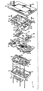
28 exploded pC.~pC~,liVC view~ :
Switch 10 is gcncrally compriscd of a back box 12, a printed circuit board
8~ ~PCB) 14, a strap 16, slidc arrangcmcnt 18, on-off button 20, framc 22, and
5~ front covcr 24~ ~sck box 12 i5 simply a hard plastic cnclosurc dcsigncd to
8~ protect the interQal clcmcnts of switch 10. lt ty~ically has 8 p1urslity of
2'7 slots 13 for vcntilatjon, and holcs IS for allowing psssagc of wircs 17~ PCEI
a8 14 is used as a substratc for mounting thc various elcctrical cc r~rerts of
29 switch 10~ Thc SpcciriC clcctrical components uscd for control switch 10 arc ~:
not relevant to the presen~ application inasmuch 8S thc fcsturcs ~ closed
51 herein arc primarily Or a mcchanical naturc~ Morcovcr, the invention as
~2 claimcd could covcr a widc variety of particular clcctrical dcsigns~ Ncverthc-
3g lcss, for complctcness, an example of the elcctronics nccessary for switch 10
34 is sho~vn in Figurc 6. Figure 6 is 8 representation of thc elcctrical
)
1332958
~ rc of a high-wattage control switch. I~he main power line is supplied via
2 line wire 200. In the preferred ' '- , switch 10 runLc off a 120 volt
AltPrnAtlne current power supply. A contact is shown int~ LL ~ the line power,
4 the contact being butt contact 112, ~ic~lccpd in detail further below. An inductor
202, rArArtitnr 204, and resistor 206 are supplied for ~ power surgec.
8 N~xt, a DC power supply is formed by diode 208, rPcictnrC 210 and 212,
7 trAncictnr 214, Zener diode 216, and r~r~ritnr 218. Tbe DlC power is used by the
8 power rP~IlAtnr 238, which is rrpfPrphly ' .1~ ' by an intPp,rAtP~ chip. The
9 power rP~llAtnr 238 provides voltAge rPE~Ilr~inn and du q cycle control for the power
0 switch triac 240, and provides ~ i ~ power for the light tt1ne diode (LED) 122
1 1 ac ~icrllCcP~ below. The negative side of r~rAritnr 218 is rnnnPrtP~ to ground 220.
1 2 Another r~rAritnr 222 is u_ed as a filter for the five volt powPr going to power
13 rF~IlAtnr 238 and LED 122.
14 In the prPfPrnp~ switcb 10 is a LL.~c _ ~ switch, havLng a line 224
for reT~te activation. Llne 224 passes thro4gh a diode Z 6, which merely acts as a
13 half-wave rert-iflpr~ and then thro4gh resistor 228. A r~rAritnr 230 smooths out the
17 rPrtifle~ signal from re~ote line 224. Also attached to this line is a resistor 232
18 and - y contact switch 120. As ~icrllccP~ below, contact switch 120 is used to
19 provide complete on-off r~rAhillty to switch 10.
l~he next element of interest is LED 122. As ~1C~ICCP~ below, LED 122 is used to
21 ill the on-off button on switch 10, so that it may thereby be located in the
22 dark. LED 122 utilizes DC voltage which was created at trAnciRtnr 214 and passed
thlY~4~h power rP&~IlAtnr 238. TrAnclRtnr 234 and resistor 236 are also used to
2~ provide power to LED 122.
2~ Power to the load (an i.. _ .~ c~ l light bulb) is Pcc~ntiAlly regulated by power
2~ rP~ tnr 238 and a triac 240. r~rA~ltnr 242 provides a sawtooth waveform to
27 trAnclctn~ 234 for timLng plnrrnCPc A variable resistor 88 (~iRrllcRP~ further
28 below), along with a tricmlng resistor 244, controls the output of power rP~IlAtnr
29 238. In turn, power rP~IlAtnr 238 controls activation of helper triac 240, ~hich
5 turns on silicon controlled rertifiPrc 246 and 248, ~ 1; ~ on the polari q of the
5 ~ current. Ihe rP~IlAtP~ power is then passed to load line 250.
5 2
Il 5
~ .
! i
1332~8
For further dctails of thc circuit-y rcquired for power limiting switches,
-
attcntion is directed ta U.S. Patent No. 4,087,702 entitled ~I)igital Elcctronic
Dimmer," and U.S. Patcnt No. 4,408,150 entitled "Specd Control System and
4 Method for Electric Motor ".
Strap 16 is prefcrably metallic, and is uscd to sccure the entire switch
10 to an elcctrical supply bo~ mounted in the wall. Strap 16 also serves a
7 heat sink for certain electrical components. Slide arrangement 18 and on-off
8 button 20 provide for manual adjustmcnt of the powcr transmittcd through
9 switch 10, and are discusscd further bclow in conjunction with Figures 3A-
3D and FiRure 5. Framc 22 acts as a guide for slide arrangement 18, and
1 l also holds on-off button 20 in ptace. Front cover 24 serves as ornamentation,
~ 2 and is affixed to switch 10 by means of scrcws 26 which pass through holcs
13 28, and then through holes 30 in strap 16. Front cover 24 typically has
14 bevelcd cdges 2S for a more pleasiDg appearance. A large rectangular cutout
27 rcceives frame 22.
lB Frame ~emblv
~ 7 Frame 22 has certain othcr features which provide a distinct advantage
18 in the assembly oî switch 10. Frame 22 emplo)~s a plurality of snaps or cl;ps
19 and posts which may be used to hold all of the components of switch lO
together, c~ccept for back box 12 and covcr 24. First of all, frame 22 has a
21 pair of short clips 32 which are uscd to join framc 22 to strap 16. Clipt 32
22 pass through holes 34 in strap 16, and thc toothed cdges 36 of clips 32
a5 catch thc inner confines of holcs 34, thereby firmly securing slide arran8ement
24 18 and on-off button 20 bctwccn frame 22 and strap 16. The length of clips
2~5 32 depends on the thickness of slidc arrsngement 18 and button 20, as well
2~ as thc thickncss of strap 16.
27 A second set of clips 38 extcnd from framc 22, through boles 40 in s~rap
28 lC, and abut notches 42 in PCB 14. Thc toothed cdge~ 44 of clips 38 cstch29 thc insidc boundary of notches 42, thereby sccuring frame 22, slide arrangemcnt
S0 18, button 20, strap 16, and PCB 14 into a singlc integral unit. The length
51 of clips 38 also depcnds on thc thickncss of fra~e 22 and strap 16, as well
52 as the hei8ht of the componcnts on PCB 14. In addition to clip~ 38, a pair
.~
13329~8
of posts 46 e~ctcnd downward from frame 22, through another sct of holes 48
5l in strap 16. Posts 46 have pegs S0 at their ends whieh fit within tiny
apertures S2 in PCB 14. This faeilitates propcr alignment of PCB with the
4 other elements Or switeh 10. Posts 46 also serve to maintain an adequate
~5 clearanee between PCB 14 and strap 16, to aeeommodate the eleetrical
components mountcd on PCB 14. It should bc noted that, whi}e elips 32 arc
7 plaecd along the Icngth of frame 22 and elips 38 arc plaecd along its width,
8 thc ctips may be placed nearly anywherc along framc 22 to achicvc the
9 aforcstatcd goals.
As previously alludcd to, the various clips and posts on frame 22 serve
ll a specific purpose which is now explained. In the assembly of control switches,
1:~ each unit is ty~ically tested immediately before packing to insure quality
13 control. However, if a defective unit has been eompletely assembled, i.e.,
14 the baek box and front cover are attached to the mounting strap, then e~ternal
ltS eoverings must be removcd in order to determine thc defcct. In a mass
proauction setting, this c~tra efrort involved in fixing thc defceti~e unit is
17 multiplicd a hundredfold, significantly raising labor costs. By utilizing the
18 novel structurc of frame 22, this extra eost can bc avoided, sinee frame 22l9 nOJas all ot the mechanicaJ and electrical components seeurcly without thc
need of attaching back bo1~ 12 or eover 24. Thus, the units may be pre-tested
21 ana, if neeessary, repaired beforc baek box 12 and eover 24 are added.
8a Units which pass final testing may thcn be complcted by attaehing baek bo~
12 to framc 22 by means of sercws S4. Screws S4 cntcr holes 5S in flanged
24 portions 56 of frame 21, thcn through holes 52 on strap 16, and sre sccured
a~ in holes S7 of baek bo~ 12.
2~ Frame 22 may bc metallie, but it is preferably" injcetion-moldet plastie.
27 In the prcferred embodiment, frame 22 has a partition S8 whieh scparates
a8 f ramc ZZ into two portions, one rcceiving slide arrangement 18 and thc other
29 reeeiving on-off button 20. Frame 22 further has two inwartly-dircctcd
flangcs S9 for seeuring slide arrangement 18 therein, and a elip 61 for holding
51 light piping 116 in place (diseus~ed further below).
32
1332~8 ~
Slide Arran~em~lt
2 Another novel featurc of the prctcnt invcntion conccrns slide arr~lng~ r-~t
3 18, which i5 shown in scvcral vicws in Figurcs 3A-3D. Slidc arrsngemcnt 18
4 is comprised of slidc base 60, slidc toppcr 62, and slide clip 64. Slidc basc
60 is a gcnerally cctangular~ planar mcmbcr, having two sidc cdges 66, a
rail 70, and flangcd cnd pieces 72. Slidc topper 62 is obloDg in shape, having
7 a concavity 74 along its rcar surface, and two small clips 76. Both slidc
8 b8sc 60 and slide toppcr 62 are prcfcrably constructcd of a hard plastic.
8 The physical dirnensions of slide base 60, as well as slide topper 62, may
vary considerably, ~ut in thc prcferrcd embodiment, slidc base 60 is approxi-
11 mstcly six centimetcrs lon~ and three centimetcrs wide, and slide toppcr 62
12 is also appro%imately thrce ccntimeters wide. End pieccs 72 assist in sccuring
1-~ button 20 withisl frame 22. Button 20 al50 hao flangcd wings 6~ to keep
14 button 20 from cscaping through thc forward portion of frame 22.
16 Slide clip 64 is also oblong in shapc, gcncrallY matching the length snd
1~ width of slide topper 62. Slide clip 64, howcver, Is a thin metallic strip,
17 whose cnds 78 havc been bent into 8 gcnerally U-shapcd c-oss scclion. In
18 this manncr, the ends 78 of slide clip 62 may wrap around thc edges 66 of
19 slide basc 60, allowing slidc clip 62 to slidably movc along thc length of
slide base 6û. The cnds 78 of slide clip 62 also hsvc a flangcd portion 80
21 which can best bc secn in Figure 3C. Each of the flsnges 80 has a small
a2 cutout which reccivcs a clip 76 of slide toppcr 62. Thus, slidc toppcr Js
sccurely~ yet slidably, mounted to slidc basc 60. Slide clip 64 rurther ha~ a
24 raised portion 82 with a gcnerally rcctangultr cutout 84, As shown in Figurc
a~s 2, as wcll as Figurcs 4A and 4~, two prongs 86 of a varjablc resistor 88
2B e~ctcnd upwardly through a slot 90 in strap 16, and thcnce to cutout 84.
27 Consequently, whcn slidc topper 62 is manually adjusted, prongs 86 move
28 along variablc rcsistor 88 which, with appropriatc electronics, altcrs the
29 firing point for the triac circuit controlling power output.
There are scveral novel featurcs in slide arrangement 18 which prcscnt
31 distinct advantagcs ovcr thc prior art. First of all, thc thinncss of slide
32 I clip 64 results in a virtually invisiblc link between slide topper C2 and the
~~8
13329~8
internal circuitry of swilch 10, imparting a supcrior acsthetic dcsign. Slidc
a arran8emcnts in thc prior art which havc a similar fi~ced slide base, have
:1 always required a large, unsightly 8aP between thc basc and the frame or
4 cover. Altcrnativcly, prior art slidc arrangcmcnts in which thc slidc basc
b movcs always leave a gaping hole at thc top or bottom of the slidc arrangcmcnt
~S whenever the slide is moved to an cxtreme position, actually rcvcaling thc
~7 inside of the switch.
8 The sccond advantage Or slidc arrangcmcnt 18 rclatcs to indcntations or
9 dimples Placcd near the cnds of slide c1ip 64. As cxplaincd abovc, a thin
strip of metal is dcsirablc for linking slidc toppcr C2 to prongs 86; howevcr,
11 thc inventors found that the U-shsped design of ends ~8 causcd exccssivc
~2 friction bctwecn slidc clip C4 and slidc basc 60. This difficulty was obviatcd
by the use of dimplcs 92. In the prcferrcd cmbodimcnt, thcre are a total of
14 six pairs of dimplcs 92, thcre being three pairs at cach cnd 78. The first
1~5 pair is locatcd along the front surrace of clip 64, protruding toward basc 60.
1~ 1n this manner, clip 64 is slightly dislocatcd from basc 60. Thc second pair
17 lies along thc outsidc of the U-shapc portion of edgc 78; these dimples alleviatc
18 friction caused by isometric tension along the Icngth of clip 64, The third
19 pair contacts the upper side of basc 60. Thus, frictional sliding forccs are
cssentially eliminated since clip 64 contacts base 60 only at the tips of dimples
21 92.
2~ The third advantsgc of slidc arrangcmcnt 18 involves rail 70. Obviously,
if raiscd portion 82 of clip C4 wcre to bc accidcntally flattened, it would not
a~ engage prongs 8C, rendering switch 10 useless. To avoid this possibility,
2~5 raised portion 82 partially rides on rail 70~ as clearly shown in Figure 3C
S#~ A final advantage of slidc arrangement 18 is that all of its components (i.e.,
27 base C0, topper 62, and c1ip 64) are easy to manufacture and as~cmblc.
28 The ncxt novel fcaturc of thc prcsent invention pcrtain5 to an air 80P
29 lever 100 which is shown in Figurc 2, but is more aptly dep;cted in Figures
4A-4C. Air gap levcr 100 consists of a gcncrally disk-shaped body having an
31 exposed lever arm 102 and a contact Icver srm 104. Contact levcr arm 104
32 further has a latcral cam surfacc 106 indicated by thc dashed lines within
Il 9
13329~8
arm 104 in Figures 4A and 4B. Air gap lever 100 is not fi~edly attachcd to
2 any other element, but rather is loosely held by frame 22. More accurately,
frame 22 has a slot 108 formed along onc sidc, and lcvcr arm 102 is positioncd
4 in slot 108.
Air GaD ~ ~ver
~S Slot 108 and lever 100 are both situated above an actuator arm 110 of
7 a butt contact 112. Cam surface 106 is forcibly urged a8ainst actuator arm
8 110. For reasons cxplaincd bclow, thc circuitry of switch 10 is designcd
9 such that, whcn contact 112 is open, the external power supply to ~witch 10
is totally cut off. When switch 10 is packed for shipping, air gap lever 100
ll may be placed in the position shown in Figure 4A, with exposed arm 102
12 extending forward from slot 108, and with contact arm 104 e~ttended to its
13 maximum reach, meanin8 thst contact 112 is open. Thus, when thc unit is
14 connectcd to the electric supply wircs, there is no dan8er of electrical shock
~ from touching the e%posed wiring. Then, when front cover 24 is placed over
l~ switch 10 (the last steD in installation), the rear surfacc of front cover 24
17 pushes exposed arm 102, rotating air 8aP lever 100 to the position shown in
18 Figure 4B. This closes contact 112, allowin8 the unit to opcrate normally.
l9 Thus, air gap lever 100 clearly provides a valusble safety measure in the
installation of switch 10. Furthermore, air gap level I00 may be reset to its
al open position if the switch 10 nceds to bc removed from the wall. A spring
22 or other bias means (not shown) may be used to automatically open lever 100
if front cover 24 is removed.
24 Li2ht pjDjn~ Button
:2~S The final innovative feature of thc prcsent invcntion is found in thc
5~ intcraction of on-off button 20 with thc clectrical circuitry of switch 10.
27 Button 20 basically consists of rectangular button member l14, and light
28 piping 116, as shown in Figurc 2. Button mcmber 114 has a holc 118 thercin
29 through which a portion of light piping 116 cxtends. Thc lowcr cnd of light
:50 piping 116 abuts a momcntary contact switch 120 mountcd to PCB 14, as
51 depicted in Figure 5. Immediatcly adjaccnt to both momentary contact 120
32 and light piping 116 is a light-emitting diodc (LED) 122. By means of this
13329~8
uniquc arrangement, the structural membcr which couplcs button 20 to thc
a elcctronics of switch 10 simultaneously acts as 8 li8ht CoQdUit SO that button
S 20 may bc found in a dark room. In thc preferred cm~odimcnt, the distal
4 tip 124 of light piping 116 is cut at a skewed anglc (4S ') so that the light
tS from LED 122 is reflected within piping 116 upwsrds toward hole 118. Thc
B uppcr portion of light piping 116 prcferably has a rough tcxture to better
7 disperse the light. The circuitry of switch 10 is preferably designed so that
8 LED 122 wi}l enersize only whcn momentary contact switch 120 is in an
9 open state (i.c., there is zero power output from switch 10).
Although the invcntion has been dcscribcd with refercnce to specific
ll cmbodimcnts, this description is not meant to be construed in a limitiDg
12 sensc. Various modifications of the discloscd embodiment, as well as altcrnative
13 embodiments of the invention will become apparcnt to persons skilled in the
14 art upon reference to the description of thc invcntion. It is thercfore
l~ contemplated that the appendcd claims will cover such modifications that fall
113 within the truc scope of thc invention.
17
18
19
21
22
24
a~
27
28
29
31
52 ~j
l l