Note: Descriptions are shown in the official language in which they were submitted.
- 133341~
01 This invention relates in general to radio
02 frequency (RF) signal processing, and more
03 particularly to a device for suppressing a strong
04 RF jamming signaL in order to extract a relatively
05 weak information signal transmitted simultaneously
06 with the jamming signal, independently of any
07 frequency separation between the strong and weak
08 signals.
09 Various types of radio frequency signal
processing devices, such as Instantaneous Frequency
11 Measurement (IFM) receivers or Digital Frequency
12 Discriminators (DFDs), have been developed to detect
13 specific RF signals in dense signal environments
14 characteristic of electronic warfare. It is well
known from the field of Electronic Counter Measures
16 (ECM) to transmit a relatively weak information
17 signal, (e.g. Radar) in the presence of a strong
18 jamming signal having the same frequency as the
19 information signal. Thus, ECM systems are designed to
render extraction of the information signals extremely
21 difficult, without knowing the jamming signal
22 frequency.
23 Electronic Support Measurement (ESM)
24 devices have been developed for extracting such
relatively weak information signals in the presence of
26 a strong jamming signal. One prior art approach
27 consists of using a band-stop (or notch) filter for
28 separating the information and jamming signals on the
29 basis of small frequency differences therebetween.
The band-stop filter is tuned to the frequency of the
31 strong jamming signal, thereby attenuating it and
32 allowing extraction of the information signal.
33 Obviously, this prior art approach
34 requires a predetermined minimal amount of frequency
separation between the jamming and information
36 signals in order to attenuate the former without
37 attenuating the latter. Thus, the previous approach
38 - 1 -
1 333~I 3
01 suffers from two main disdvantages. Firstly,
02 attenuation of the strong jamming signal is frequency
03 dependent, such that in the event the frequency
04 separation between the jamming and information signals
05 is not sufficiently large with respect to the filter
06 bandwidth, the information signal will suffer a
07 certain amount of attenuation. Therefore, in the
08 event the information and jamming signal frequencies
09 are identical, the prior art approach cannot be used.
Secondly, in the event the frequency of the strong
11 jamming signal is unknown, the ESM device must first
12 measure the jamming frequency and then tune the
13 filter. Most ECM systems transmit jamming and
14 information signals at a continuously variable
frequency, according to a pseudorandom pattern, making
16 frequency detection prior to filter tuning extremely
17 difficult.
18 According to the present invention, a
19 frequency independent strong signal suppressor is
provided for suppressing a strong jamming signal in
21 order that an information signal may be extracted
22 for additional signal processing. An amplitude
23 dependent Voltage Standing Wave Ratio (VSWR) device is
24 utilized for receiving an incident RF signal (e.g. a
combined jamming and information signal), absorbing
26 the jamming signal and reflecting the information
27 signal for reception by an external signal processing
28 device. Signals having amplitudes greater than a
29 predetermined threshold (i.e. jamming signals) are
absorbed while weaker signals (e.g. radar signals) are
31 substantially reflected by the amplitude dependent
32 VSWR device.
33 Hence, according to the present invention,
34 information signals which are transmitted in the
presence of strong jamming signals, may be extracted
36 regardless of the relative frequencies of the
37 information and jamming signals. The device of the
38 - 2 -
` 1333~
1 present invention operates instantaneously on received
2 signals, thereby overcoming the disadvantage of the
3 prior art approach which typically required a
4 predetermined amount of time in order to detect the
S jamming signal frequency and thereafter tune a notch
6 filter to the detected frequency. The device of the
7 present invention is of extremely simple design, and may
8 be advantageously and inexpensively fabricated on a
9 small hybrid circuit.
An important aspect of the amplitude dependent
11 VSWR device is that the return loss is a function of the
12 incident signal power. In particular, the input
13 characteristics of the device exhibit a return loss
14 which approaches infinity in the presence of an incident
signal having power greater than a predetermined
16 threshold (i.e. turn-on point), and a return loss which
17 approaches O dB in the presence of an input signal
18 having power less than the turn-on point threshold.
19 In accordance with an embodiment of the
invention, a frequency independent strong signal
21 suppressor is comprised of an amplitude dependent
22 voltage standing wave ratio device for receiving and
23 substantially absorbing incident radio frequency signals
24 characterized by amplitudes greater than a predetermined
threshold and substantially reflecting signals
26 characterized by amplitudes less than the threshold, and
27 apparatus for extracting the reflected signals for
28 processing by an external signal processing device, such
29 that strong signals are absorbed and thereby suppressed
while weak signals are reflected and extracted for
31 processing by the signal processing device.
32 In accordance with another embodiment, a
33 frequency independent strong signal suppressor is
34 comprised of a hybrid having at least three ports, a
36 - 3 -
37
38
D
1333413
-
1 first one of the ports being adapted to receive and
2 couple signals to a second one of the ports, the second
3 one of the ports being adapted to receive and couple
4 signals to a third one of the ports, an input terminal
S for receiving and applying radio frequency signals to
6 the first port, such that the signals are coupled to the
7 second port, apparatus connected to the second port, for
8 receiving and substantially absorbing predetermined ones
g of the radio frequency signals having amplitudes greater
than a predetermined threshold while substantially
11 reflecting to the second port further predetermined ones
12 of the radio frequency signals having amplitudes less
13 than the predetermined threshold, such that the
14 reflected signals are coupled to the third port, and an
output terminal connected to the third port, for
16 transmitting the reflected signals, whereby strong radio
17 frequency signals having amplitudes greater than the
18 threshold are absorbed and thereby suppressed while
19 relatively weak signals having amplitudes less than the
threshold are reflected and transmitted to the output
21 terminal.
22 In accordance with another embodiment, a
23 frequency independent strong signal suppressor is
24 comprised of a hybrid for receiving signals on
respective ports thereof and unidirectionally coupling
26 the received signals to respective adjacent ports
27 thereof, the hybrid being adapted to receive signals on
28 a first one of the ports and couple the received signals
29 to a second adjacent one of the ports, an amplitude
dependent VSWR device connected to the second one of the
31 ports for receiving and substantially absorbing
32 predetermined ones of the signals having amplitudes
33 greater than a predetermined threshold and substantially
34 reflecting further predetermined ones of the signals
having amplitudes less than the threshold, and the
36
37
38 - 3a -
f~
.LJ
1333~
1 hybrid being adapted to receive the reflected signals on
2 the second one of the ports and couple the reflected
3 signals to a third one of the ports, whereby strong
4 signals are substantially absorbed and thereby
s suppressed while weaker signals are substantially
6 reflected and coupled to the third port.
7 In accordance with another embodiment, a
8 method for frequency independent suppression of strong
g signals, is comprised of the steps of receiving a
combined radio frequency signal comprised of a strong
11 jamming signal and a relatively weak information signal,
12 applying the combined radio frequency signal to an
13 amplitude dependent voltage standing wave ratio device,
14 whereupon the strong jamming signal is substantially
absorbed and the relatively weak information signal is
16 substantially reflected, and receiving and outputting
17 the reflected information signal.
18 A better understanding of the invention will
19 be obtained with reference to the detailed description
20 below in conjunction with the following drawings in
21 which:
22 Figure l is a block diagram of an electronic
23 warfare scenario, according to the prior art,
24 Figure 2 is a block diagram of a frequency
25 independent strong signal suppresser in accordance with
26 the present invention,
27 Figure 3 is a graph illustrating return loss
28 characteristics of an amplitude dependent VSWR device
29 utilized in accordance with the present invention, and
Figure 4 is a block diagram of a modified ECM
31 system utilizing the strong signal suppressor, according
32 to an alternative embodiment of the present invention.
33
34
36
37 - 3b -
38
I~
.J
1333~13
01 With reference to Figure 1, a typical
02 electronic warfare scenario is illustrated, wherein an
03 ECM system is shown generally as 1, and is comprised
04 of a transmitter 3 for generating an information
05 signal and a jamming signal at the same frequency, and
06 an antenna 5 for transmitting the combined signals.
07 Signals are received within the ECM
08 system via a further antenna 7 and applied to a
09 receiver 9. The receiver 9 also typically
incorporates a notch filter tuned for attenuating the
11 known jamming signal frequency while substantially
12 allowing the information signal to pass unattenuated,
13 for additional signal processing.
14 A remote ESM system 6 is shown comprised
of an antenna 11 connected to a circuit 13 for
16 detecting the frequency of the jamming signal and
17 thereafter tuning an internal notch filter to the
18 desired frequency. For instance, a DIFM receiver may
19 be used to isolate and detect the jamming signal
frequency. The tuned notch filter then substantially
21 attenuates the jamming signal while transmitting the
22 information signal to an external signal processing
23 device 15.
24 As discussed, prior art combined DIFM and
notch filter circuits suffer from a number of
26 disadvantages, such as the time required for detecting
27 the jamming signal frequency, and inadvertent
28 attenuation of the information signal in the event of
29 only a small, or no frequency separation between the
jamming and information signals.
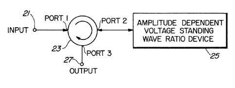
31 Figure 2 illustrates a frequency
32 independent strong signal suppressor according to the
33 present invention. Incident signals received by an
34 antenna (such as antenna 7 or 11 with reference to
Figure 1), are applied to an input terminal 21 and
36 transmitted therefrom to an input port (Port 1) of a
37 hybrid circuit 23. Hybrid circuit 23 translates
38 - 4 -
133~3
01 signals received on Port 1 to a second port (Port 2),
02 for reception by an amplitude dependent Voltage
03 Standing Wave Ratio (VSWR) device 25, discussed in
04 greater detail below with reference to Figure 3.
05 Signals output from VSWR device 25 and applied to Port
06 2 are translated from Port 2 to be output from a third
07 port (Port 3) of the hybrid circuit 23, for further
08 application to an output terminal 27.
09 According to a preferred embodiment,
hybrid circuit 23 is comprised of a microwave
11 circulator, which is a component for acting on the
12 magnetic field of an incident signal such that
13 signals received on Port 1 are unidirectionally
14 translated to Port 2, signals received on Port 2 are
unidirectionally translated to Port 3, and signals
16 received on Port 3 are unidirectionally translated to
17 Port 1.
18 With reference to the graph illustrated in
19 Figure 3, operation of the amplitude dependent VSWR
device 25 (Figure 2) is described in greater detail.
21 The device is seen to be characterized by an abrupt
22 change in return loss relative to the incident signal
23 amplitude, (i.e. power). Thus, for incident signals
24 having amplitudes less than a predetermined threshold
(designated as the turn-on point), the device 25 is
26 characterized by a return loss of A dB (which ideally
27 approaches 0 dB). Conversely, for incident signals
28 having amplitudes greater than the turn-on point
29 threshold, the device 25 is characterized by a return
loss of B dB (which ideally approaches infinity).
31 As can be seen from Figure 3, the return
32 loss characteristics of the amplitude dependent VSWR
33 device 25 exhibit a steep increase in the return loss
34 (vertical, on the ideal case) for signals having
amplitudes greater than the turn-on threshold. In the
36 event of incident signals having amplitudes within the
37 designated "area of ambiguity" on either side of the
38 - 5 -
- 1333~1~
01 turn-on point threshold, the return loss is mid-way
02 between substantial reflection (A dB) and substantial
03 absorption (B dB). The variation in return loss for
04 signals above and below the turn-on point threshold,
05 is designated by the term "suppression factor".
06 In operation, combined radio frequency
07 (e.g. microwave) information and jamming signals are
08 received on input terminal 21 from an antenna (e.g.
09 antenna 11 or 7 in Figure 1). The received combined
RF signals are applied to Port 1 and circulated to
11 Port 2 and transmitted therefrom to the amplitude
12 dependent VSWR device 25. Typically, the jamming
13 signal is characterized by an amplitude greater than
14 the turn-on point threshold of device 25 while the
information signal is characterized by an amplitude
16 significantly less than the turn-on point threshold.
17 Thus, as can be seen with reference to Figure 3, the
18 VSWR device 25 exhibits a large return loss (e.g. B
19 dB) with respect to the jamming signal, and a low
return loss (e.g. A dB) with respect to the
21 information signal. In other words, the device offers
22 a substantially perfect match in impedance to the
23 jamming signal and a substantially mismatched
24 impedance to the information signal. Therefore, the
jamming signal will be substantially absorbed by
26 device 25 while the information signal will be
27 substantially reflected.
28 The reflected information signal is
29 applied to Port 2 of hybrid 23, circulated to Port 3,
and transmitted therefrom to output terminal 27
31 connected to an external signal processing device
32 (e.g. device 15 or 9 with reference to Figure 1).
33 In the event both the incident jamming and
34 information signals are characterized by amplitudes
less than the turn-on point threshold of the device
36 25, the signals may be amplified prior to application
37 to the input terminal 12 in Figure 2. Also, a
38 - 6 -
-
1~33~1~
01 plurality of signal suppressors can be cascaded in
02 series, with signal amplifiers disposed between
03 successive ones thereof.
04 Conversely, in the event both the jamming
05 and information signals are characterized by
06 amplitudes which exceed the turn-on point threshold,
07 an attenuator may be connected to the input terminal
08 21 for sufficiently attenuating both signals in order
09 that the jamming signal remains above the turn-on
point threshold while the information signal is
11 reduced to less than this threshold.
12 The device according to the present
13 invention absorbs or reflects RF signals only on the
14 basis of amplitude, independent of frequency. Thus, a
relatively weak information signal can be extracted
16 even in the presence of a strong jamming signal of the
17 same frequency.
18 The amplitude dependent VSWR device 25 is
19 preferrably one of a variety of non-linear radio
frequency devices, such as detectors, limiters,
21 frequency doublers or dividers, etc. However, if the
22 difference in amplitude between a pair of incident
23 jamming and information signals is less than the area
24 of ambiguity characteristic of the device, the device
will not function properly. Accordingly, in order to
26 minimize the area of ambiguity (to preferably less
27 than 20 - 30 dB), a device having an abrupt change in
28 return loss is preferred, (i.e. as shown in Figure 3).
29 According to the preferred embodiment,
amplitude dependent VSWR device 25 was comprised of an
31 anolog microwave frequency divider manufactured by
32 Telemus Electronic Systems Inc., and sold under the
33 trademark Halver~. The Telemus frequency Halver~
34 circuit is described in greater detail in Canadian
Patent 1,041,614 entitled "BROAD BAND FREQUENCY
36 DIVIDER USING MICROWAVE VARACTORS", as well as in the
37 following issued Canadian Patents: 1,085,925 entitled
38 - 7 -
1333~
01 "APPARATUS FOR MEASURING THE FREQUENCY OF MICROWAVE
02 SIGNALS"; 1,111,114 entitled "MICROWAVE DIVISION BY
03 PHASE LOCK LOOPS"; 1,124,337 entitled "MICROWAVE PHASE
04 LOCK LOOPS USING FET FREQUENCY DIVIDERS"; 1,105,574
05 entitled "BROAD BAND MICROWAVE FREQUENCY DIVIDER FOR
06 DIVISION BY A NUMBER GREATER THAN 2"; 1,118,849
07 entitled "WIDE BAND MESFET MICROWAVE FREQUENCY
08 DIVIDER"; 1,121,006 entitled "BROAD BAND FREQUENCY
09 DIVIDER" and 1,119,702 entitled "PARAMETRIC FREQUENCY
DIVISION".
11 While the present invention may be
12 advantageously utilized within ESM systems, an
13 alternative application of the invention is directed
14 to ECM systems. Prior art ECM systems, such as shown
in Figure 1, have utilized separate transmit and
16 receive antennas 5 and 7. This is a result of the
17 requirement that a sufficient degree of isolation
18 (e.g. typically 120 dB) must be maintained between the
19 transmitter 3 and receiver 9 in order to allow the
jamming signal to disperse and thereby become
21 attenuated in order to receive the information signal
22 without requiring use of a notch filter.
23 The requirement of separate transmit and
24 receive antennas has been found to be a significant
disadvantage in terms of cost and complexity.
26 Furthermore, in certain environments, such as on
27 ships, it is usually quite difficult to accommodate
28 two separate antennas with the requisite amount of
29 separation.
According to the alternative application
31 of the present invention, an ECM system is provided
32 with reference to Figure 4, comprised of a transmitter
33 3 connected to an antenna 5, a hybrid 23 (e.g.
34 circulator) connected through Port 1 to the antenna 5,
an amplitude dependent VSWR device 25 connected to
36 Port 2, and a receiver 9 connected to Port 3 of the
37 hybrid 23.
38 - 8 -
1~33~
01 In operation, the strong signal suppressor
02 comprised of hybrid 23 and VSWR device 25 extracts an
03 information signal received from antenna 5, even in
04 the presence of a strong jamming signal, such that no
05 isolation is required between the transmitter 3 and
06 receiver 9. Hence, only a single antenna 5 is
07 required for both transmission and reception,
08 resulting in considerable savings in cost and
09 complexity of the ECM system.
In summary, the strong signal suppressor
11 according to the present invention provides virtually
12 instantaneous extraction of a weak information signal
13 in the presence of strong jamming signal independently
14 of signal frequency and without requiring expensive,
complex and slow IFM and notch filter circuitry as in
16 the prior art.
17 A person understanding the present
18 invention may conceive of other embodiments or
19 variations therein. For example, as discussed above,
hybrid 23 is preferably a microwave circulator.
21 However, other appropriate hybrid circuits, such as
22 directional couplers, etc., may be utilized. Also,
23 while the amplitude dependent VSWR device 25 was
24 comprised of a frequency Halver~ circuit in the
preferred embodiment, most non-linear radio frequency
26 devices such as detectors, limiters, frequency
27 doublers, type-C amplifiers, or frequency dividers may
28 be utilized. However, the device 25 must be
29 characterized by a relatively sharp or abrupt
turn-oncharacteristic resulting in a small area of
31 ambiguity, and must also present a perfect match (high
32 return loss) only for signals having amplitudes
33 greater than the turn-on point threshold.
34 All such embodiments or variations are
considered to be within the sphere and scope of the
36 present invention as defined by the claims appended
37 hereto.
38 _ 9 _