Note: Descriptions are shown in the official language in which they were submitted.
1333422
OPTICAL DISK DRIVE SYSTEM
BACKGROUND OF THE INVENTION
The assignee herein is also the assignee of U.S. Patent
4,864,536 entitled "Optical Memory Method and System," and U.S.
Patent 4,915,982 entitled "Thin Film Photoluminescent Articles and
Method of Making Same."
The present invention relates generally to mass storage
devices for data storage. More particularly, the present
invention relates to a method of and apparatus for mass data or
information storage utilizing purely photoelectronic processes for
writing, reading, and erasing stored data.
Optical storage devices presently known generally permit
two or three orders of magnitude more data to be stored per disk
than with magnetic methods and apparatus. Because of the
potential for much greater storage of data and also because of the
enormous projected market for such optical memories, active
development of optical storage devices is currently occurring in
several different directions. Such activities are directed
1333422
towards read-only, write-once-read many times (WORM) and erasable
optical memory systems. While read only and WORM optical memories
are already available, erasable optical memory systems have
encountered much greater developmental difficulties than read-only
WORM systems because the qualities of the storage media required
present problems of much greater technical complexity.
Read-only optical memory devices for use as computer
peripherals, such as CD-ROMs, became commercially available with
the advent of the digital audio compact disk. Current disk data
storage capacity for such units is 200-600 megabytes. Such disks
are factory fabricated using a molding press and metalizing
operations and are suitable for low cost distribution of large
fixed database information.
WORM devices allow the user to encode his own data on the
disk, however only once. Data bits are stored at physical
locations by irreversibly "burning" the medium with a laser. Such
permanent encoding can be read back indefinitely, thus making WORM
technology suitable for archival storage of large quantities of
information, including digitized images, where random access to a
large database is desirable.
It is the third category of optical disk storage devices,
namely erasable storage devices, that is believed to embody the
greatest utility for mass storage purposes. Such devices will be
competitive with present magnetic tape and disk mass storage, and
1333422
will have a major impact on computer technology in the years
ahead. At present, the three most active approaches now being
pursued for erasable optical storage involve magneto-optical
material systems, dye polymers, and techniques that produce
crystal structure or phase transformation in the storage medium at
the spot being written to. All of these approaches require heat
which usually changes the physical or chemical structure of the
materials in performing the write or erase function. Thus, the
time to write data to such systems is dependent upon a certain
"dwell" time during which the spot to which data is being written
must be heated or otherwise physically transformed.
Another drawback with such approaches is that media
performance is highly sensitive to impurities, impurity diffusion,
oxidation, and other imperfections that propagate into defects and
that only show up after multiple switching cycles or at times
later than the manufacturing and testing of the devices. Of the
three approaches discussed above, progress has been greatest with
magneto-optic materials. Laboratory results in this area have
reported millions of write/erase cycles. See, for example, H-P.
D. Shieh Ph.D. Thesis, Carnegie-Mellon University, Pittsburgh,
Pennsylvania (1987).
In order to utilize erasable optical media for mass
storage, the optical media must be fast enough to be marked at
high data rates using low power lasers. The media must also
maintain almost error-free data at acceptable computer industry
- 3
1333~22
standards for at least ten years, for example, no more than one
uncorrectable error in 10 bits. Thus, finding the right
physical phenomenon to serve as the basis for erasablity in a
high-speed, high-resolution optical storage medium for use with an
optical disk storage system has been very difficult. Most of the
effort in this area over the past ten years, as described above,
has gone into the use of magneto-optic materials. However, the
commercial realization of erasable magneto-optical storage has not
yet been achieved, nor are there yet any guarantees that it ever
will be. Unfortunately, the performance of the other approaches
discussed above generally is not comparable.
In order to overcome the problems of the prior art, and
provide a basis for a workable optical disk storage system, a new
approach to the optical storage materials problem which satisfies
the optical media requirements of density, speed and long cycle
life has been developed. This development utilizes the phenomenon
of electron trapping in a class of new materials which comprise an
alkaline earth crystal typically doped with rare earth elements.
Thin crystalline films of such materials are formed on various
substrates, such as glass or alumina, in order to provide the disk
storage medium.
Since the trapping phenomenon is a purely electronic
process, read/write/erase operations can be performed very fast.
In addition, the physical trapping phenomenon suggests that media
life may be practically limitless. Also, the effect of electron
4 -
1333~22
traPping yields a linear response characteristic, which provides
an analog dimension to the storage capability. Thus, for example,
the potential disk storage capacity of a single 5-1/4 inch disk
could be extended to several gigabytes. Obviously, the density of
stored information is extremely high.
The materials to be used as the media for the optical
disk storage system described herein are the subject of United
States Patent 4,915,982, which is a continuation-in-part of United
States Patents 4,864,536 and 4,830,875. Other materials useful as
the storage media herein are disclosed in co-pending United States
Patents 4,839,092; 4,806,772 4,879,186; and 4,842,960. The
assignee herein is the assignee in each of those patents.
The material described in U.S. Patent 4,915,982
demonstrates an extremely linear relationship between the
write input and the read output. Thus, this capability
demonstrates a large noise margin for binary storage, as
well as the possibility of increased information storage
density when employed as an analog or multi-level digital
memory medium. Multi-level refers to the fact that by writing
with a plurality of intensities of the same laser beam,
5 -
C,.
1333422
the linearity of the resulting emissions upon being impinged by a
read laser beam is such that information can be stored and
recognized at various "levels" of intensity, for example, at .2,
.4, .6, .8 and 1 intensity. This particular media is in the form
of a thin film and can be "charged" and "discharged" with light by
exciting ground state electrons to an elevated energy level.
Specifically, upon illumination by visible light, electrons are
raised to high energy trapping states, where they can remain
indefinitely. When later illuminated by infrared light, the
electrons are released from the traps, emitting a new visible
light. Thus, with such materials, digital data is stored and
retrieved by using low energy lasers to trap and read the
electrons at a particular location.
Such solid state photonic materials have electrons having
bi-stable equilibrium states; one with electrons in a ground
state, and the other in which electrons are "trapped" in a well-
defined, specific elevated energy state. Electrons are raised to
the higher energy state by the absorption of visible light
photons, thus filling available trap sites. An electron in the
elevated energy state can be released from its trap site by
inputting sufficient energy to the electron to permit it to escape
from the well. When that occurs, the electron falls back to its
ground state and emits a corresponding visible photon. The number
of electrons in the elevated energy state is proportional to the
visible light intensity used for recording. Thus, as a result of
-- 6
1333422
such characteristics, such materials can, in effect, "store" light
energy.
The purely photo-electronic mechanisms involved in such
electron trapping materials obviate the need for any thermal
excursions and, therefore, the number of electrons trapped in the
material is inherently linear. Since localized resolution of the
"write" step depends only on the performance of the addressing
optics, an optical writing spot diameter of one micron will allow
at least 550 megabytes of storage on a 130 mm or 5-1/4" disk
coated with the thin film material as disclosed herein. With the
use of encoding techniques such as MFM, modified MFM, or record
length limiting (RLL), which techniques are commonly used with
magnetic disk recording, the storage capacity can be increased by
up to a factor of 3 over the use of FM or frequency modulation
coding. The rise and fall times associated with optical read and
write pulses are in the nanosecond range. Thus, the read and
write data transfer rates have been found to be at least 200
megabits per second for optical disk drive media utilizing
electron trapping materials.
Rotating disk memory systems require directions for the
retrieval of the stored information. One set of those directions
informs the drive mechanism where the requested information is or
will be stored. The other set provides alignment for the read/
write mechanism during processing. The alignment parameters
-- 7
1333422
include focusing, speed, tracks, and mark locations. The writing
of information is dependent upon the media used such as write
once, magneto-optic, dye polymer, or phase change, but in all
cases, involves a change in the reflection parameters in the spot
written to. The read method is based on detecting such
reflectivity changes at the surface of the disk.
The common method presently used for tracking with
reflective surface optical disks, such as the compact disc, is to
rely on a grouped track as the principal mode of aligning and
focusing the read/write head in the middle of the track. The
speed information is either contained in the repetitive pattern of
marks or in a depth modulation of the group.
Yet another tracking method presently utilized is known
as the "Sampled Servo" system. This system relies on changes in
the reflection of spots on the disk surface. The spots are
located in the manner which provide information about the track
location, the speed of the disk and the adequacy of focusing.
The erasable optical disk memory systems disclosed
herein, which rely upon a thin film of electron trapping material
as the media, do not rely on reflection for readout. Rather, the
emission of the media under infrared stimulation can be utilized
to retrieve pre-written tracking information from the disk.
-- 8
1333~2z
SUMMARY AND OBJECTS OF THE INVENTION
In view of the foregoing, it should be apparent that
there exists a need in the art for a method of and apparatus for
operating and constructing an erasable optical disk memory system
in which electron trapping material used as the storage media
permits writing, reading, and erasing essentially an unlimited
number of times. It is, therefore, a primary object of this
invention to provide a method of and apparatus for operating and
constructing an erasable optical disk drive system which is
characterized by an electron trapping media such that the write,
read, and erase functions can be accomplished with high density,
speed and without serious degradation over a large number of
erased functions.
More particularly, it is an object of this invention to
provide an erasable optical disk memory system for information
storage which is capable of storing orders of magnitude more data
per disk than inductive magnetic media systems.
Still more particularly, it is an object of this
invention to provide an erasable optical disk drive memory system
in which data is stored as light energy and which is not dependent
upon the reflective properties of the disk for effecting storage
or readout of stored information.
g
133~122
Briefly described, these and other objects of the
invention are accomplished in accordance with its apparatus
aspects by providing a disk containing a coating of thin film
electron trapping material which is rotated in a manner similar to
that of magnetic hard disk drives, also known as Winchester disk
drives. Data is read onto the disk in the form of a write laser
operating at a wavelength of visible light, preferably with
wavelengths peaking between 450 and 600 nanometers and preferably
at about 450 nanometers. A read laser is utilized to irradiate
the disk with near infrared radiation having a wavelength with
peaks between 700 and 1,450 nanometers, but preferably at about
1,000 nanometers. When stimulated by the near infrared read
radiation, any stored bits (representing, for example, a binary
one) will cause a predetermined radiation emission characteristic
that peaks in the orange light band, at about 620 nanometers.
Such a detected emission corresponds to a binary one recorded at
that point. The absence of such radiation emission characteristic
corresponds to a binary zero recorded at that point.
The optical disk memory storage system of the present
invention also includes an optical processing unit for
transmitting both the read and write laser beams to the read/write
head, as well as various detector electronics and positioning
electronics for positioning the head over the disk. Data output
and data input is handled by a standard computer interface.
-- 10 --
1333422
With these and other objects, advantages and features of
the invention that may become hereinafter apparent, the nature of
the invention may be more clearly understood by reference to the
following detailed description of the invention, the appended
claims and to the several drawings attached herein.
-- 11 --
133~422
BRIEF DESCRIPTION OF THE DRAWINGS
Figure 1 is a diagram showing the principles of operation of
the thin film storage media applied to the surface
of the disk used with the present invention;
Figure 2 is a graph showing the trap-filling efficiency of a
particular electron trapping film suitable for use
with the present invention as a function of the
wavelength of the exciting energy;
- Figure 3 is a graph showing the relative infrared
sensitivity for the read and erase functions for
the same particular electron trapping material as
Figure 2;
Figure 4 is a graph showing the wavelengths of emission from
the disk upon their infrared illumination for the
same particular electron trapping material shown in
Figures 2 and 3;
Figure 5 is a graph of the relative luminescence or read
output as a function of write energy for the same
particular electron trapping material as shown in
Figures 2-4;
- 12 -
1333~22igure 6 is a pictorial diagram of the structure of the
optical disk used with the present erasable optical
disk memory system;
Figure 7 is a schematic block diagram of the electronics and
optics necessary for reading, writing, and erasing
data onto and from the disk;
igure 8 is a pictorial partially cut-away drawing of the
optical disk storage system of the present
invention;
igure 9 is a schematic block diagram of the position servo
tracking and velocity servo tracking circuitry for
use with the optical disk drive memory system of
the present invention; and
igure 10 is a schematic block diagram of the optical
processing unit and actuator arm assembly for use
with the optical disk drive memory system of the
present invention.
- 13 -
1333~22
DETAILED DESCRIPTION OF THE PREFERRED EMBODIMENTS
Referring now in detail to the drawings wherein like
parts are designated by like reference numerals throughout, there
is illustrated in Figure 1 an explanation of the basis of the
operation of the class of optlcal storage media electron trapping
materials used with the erasable optical disk drive memory system
of the present invention. As illustrated in Figure 1, the wide
bandgap host material includes selected impurities which are
associated with energy levels ET. The narrow E band is designated
as the communication band since electron interaction is allowed
there. At level T, which is referred to as the trapping level,
the trapping sites are non-communicating because they do not allow
electron interaction.
As indicated in Figure 1, visible radiation, or charging
light, excites carriers so that they can fill the trapping sites.
The trapped depth in these group II-VI phosphors, of about 1.2
electron volts, is sufficiently above the thermal energy range of
the phosphors such that electrons cannot be dislodged by thermal
agitation. By controlling the trapped density, the tunneling
interchange at trapping level T may be cut off. Under such
conditions, the trapped electrons cannot communicate with each
other, and the possibility of recombination is thus eliminated.
When the charging radiation terminates and the electron
trapping material is in its electronically energized state, the
- 14 -
1333~2~
traps are filled, communication band E is empty, and recombination
from trapping level T to valence band G is nonexistent. As a
consequence, the electrons in the trapping level T will remain or
be "stored" there for a time which approaches infinity.
If the charged electron trapping material is then exposed
to infrared or near infrared light, sufficient energy equal to the
difference between the energy of an electron in the communication
band E minus the energy of an electron at trapping level T is
provided which serves to move electrons from the trapping level T
to the communication band E. While in the communication band E,
the electrons may interact and then return to the ground state or
valence band G. However, as the electrons return from the
communication band D to the valence band G, a photon of energy E
minus G is emitted. By the selection of an appropriate doping
rare earth element, the wavelengths of light given off by the
photon emitted when an electron falls from the communication band
E down to the valence band G can be predetermined. The sensing of
the occurrence of such an emission serves to indicate whether a
particular point being addressed on the disk surface contained a
bit (signifying a 1) or no bit (signifying a 0), or vice versa.
In contrast to the physical changes which occur by the
use of a writing laser beam in known approaches to erasable (and
non-erasable) optical storage systems, the writing and erasing of
a spot on the surface of electron trapping materials requires only
a change in the energy state of the electrons at that spot. Since
- 15 -
1333~2~
no heating is involved, latent, defect induced read, write, and
erasable forms of degradation do not occur. Consequently, the
number of switching cycles in the electron trapping material is
virtually unlimited, exceeding 10 million write/erase cycles with
no observed change in the thin film.
The filling of the traps at trapping level T requires
that a threshold energy be exceeded. A characteristic curve for
the preferred electron trapping material for use as the storage
media with the present invention, is shown in Figure 2. That
preferred material is disclosed in United States Patent
4,842,960, issued 27 June 1989, to Quantex Corporation. As shown
in Figure 2, the threshold energy level which must be exceeded
in order to fill the trapping level T begins at wavelengths of
visible light shorter than 600 nanometers.
After the traps contained in the trapping level T are
filled, impingement of near infrared radiation can cause
electrons to be released. A graph showing the relative infrared
sensitivity versus the peaks of the infrared radiation is shown
in Figure 3. In all instances, the graphs shown in Figures 2-5
are for the same material described in connection with Figure 2.
As shown in Figure 3, for the material discussed herein for use
with the preferred embodiment, the most efficient rate of release
occurs at
- 16 -
~
1333~2~
wavelengths having peaks of just under 1 micron, or at about 1,000
nanometers.
As shown in Figure 4, when the thin phosphor film
disclosed herein for use in the preferred embodiment is stimulated
by infrared radiation having peaks whose wavelengths are shown in
Figure 3, the phosphor film displays an emission characteristic
that peaks in the orange light band, at about 620 nanometers. It
should be noted, however, that Figures 2-5 are only representative
and that peak wavelengths can be altered by changing the rare
earth element dopants. In addition, the spectral widths of the
responses can also be altered within certain limits.
The number of electrons trapped in the higher energy
state at trapping level T is proportional to the amount of writing
energy incident on the surface of the thin film electron trapping
material. As shown in Figure 5, saturation is reached, for the
thin film material useful for the preferred embodiment, at a level
of about 5 milijoules per square centimeter. At lower flux
levels, linearity is observed through orders of magnitude. In
addition, the read-out emission is also linear with respect to the
intensity of the write beam. This linearity characteristic of the
electron trapping material allows such material, using the optical
disk drive system disclosed herein, to record and read back analog
signals, such as video or analog data transactions, using
amplitude modulation, which is not possible with other optical
disk drive systems.
- 17 -
133~22
If the traps contained in the trapping level T are
physically separated by more than a tunneling distance, they do
not communicate with each other and self-discharge is eliminated.
This condition corresponds to a highest density of excited
electrons on the order of about 102 per cubic centimeter. Each
time an infrared signal is applied to the charged electron
trapping film, emission of orange light occurs. Of course, with
each photon emitted, the number of electrons remaining in traps in
the trapping level T is reduced. Depending on the sensitivity of
the detector which, in this case is at 620 nanometers, many
readings can be made before the traps are depleted. For the
examples given herein, complete erasure of a bit storage spot 1
micrometer in diameter requires approximately 1 picojoule of
infrared energy. Of course, depletion can be avoided, if
necessary, by periodic refreshing of the stored data.
As briefly described above, the ability of electron
trapping materials to "store" energy received in the form of light
and to later release that energy upon interrogation by another
light beam, comprises the means of digital switching used by the
storage media of the present invention. Data points on the
storage media surface that have electrons trapped in the elevated
state can be interpreted as "on" or a binary one, while those with
no electrons in the elevated state are interpreted as "off" or
binary zero. Conversely, changed data points can be interpreted
- 18 -
1333~22
as "zeros" and unchanged data points as "ones". It is also
possible to "charge" the entire disk with visible light and to
write data using the infrared read beam. In that case, the ones
or zeros would be stored on the disk at points which have been
discharged and vice-versa. Also, only a single infrared beam
would be necessary to both read and write data.
Since at each such spot there are sufficient electrons
that can switch energy states, the present invention optically
determines whether a spot is a binary zero or one without altering
the "switch" setting. That is accomplished by interrogating the
spot with an infrared beam of low intensity in order to release a
small fraction of the elevated energy electrons, enough to
determine whether or not the spot is a binary one or binary zero.
However, as a practical matter, not enough of the elevated energy
electrons are released to significantly deplete the inventory of
energized electrons stored at that spot. Utilizing the particular
electron trapping thin film materials discussed herein for media
storage, switching or write/erase speeds of 5 nanoseconds or less
are achieved.
It is also possible to coat multiple layers of
differently doped electron trapping materials, one on top of the
other. Since each layer produces a different wavelength of output
emission, it is possible to separate the read beam signals on that
basis. Binary codes can additionally be used to distinguish
between layers.
-- 19 --
133342~
In addition, the read, write and erase laser power
requirements for the present invention are low. It is sufficient
for the write energy to be a fraction of 1 picojoule per cubic
micron, for example, about 0.5 picojoule per cubic micron. The
read energy is at femtojoules, for example, about 10 femtojoules
per cubic micron. The erase energy is about 1 picojoule per cubic
micron. In watts, the write laser power is preferably about 0.1
mW, the read laser power about 0.5 mW and the erase laser power is
preferably about 2.0 mW.
Figure 6 is a side view of an optical disk showing the
disk substrate 12 upon which the electron trapping layer 16 is
deposited. The disk substrate 12 is preferably made from an
optical alumina material. However, it could also be made from
other materials such as optical glass, which can be readily coated
with a thin film material and withstand the temperatures necessary
to fuse the crystalline structure of the thin film material. The
first material deposited onto the disk substrate 12 is an
interlayer material 14 with a thickness of about several hundred
Angstroms. The purpose of this interlayer 14 is to define a
crystalline surface structure for the electron trapping layer. It
also provides a chemical barrier to prevent any leaching of the
substrate material into the electron trapping layer 16. Any
suitable material, such as CaO, MoO3 or ZnS may be used, however
ZnS is preferred. Any suitable deposition process may be
utilized.
- 20 -
1333~2~
The second layer deposited on the disk 10, on top of the
interlayer 14, is the electron trapping layer 16. The thickness
of the electron trapping material 16 is preferably about 5
microns. The deposition processes described in the United States
patents noted earlier may be used to deposit this layer onto the
interlayer 14 already deposited onto the disk substrate 12.
A third or protective layer 18 is sputtered, evaporated,
electron beam deposited or laid down on top of the electron
trapping layer 16 by any other known deposition method. The
protective layer 18 serves to chemically protect the electron
trapping layer 16 from chemical contamination. It chemically
seals the electron trapping layer 16. The protective layer 18
also serves to provide an optically clear coating over the
electron trapping layer 16. It may preferably be comprised of
aluminum oxide or some other suitable material.
A fourth layer 19 of plastic or some other optically
clear sealing material may optionally be used to coat the
protective layer 18. This coating layer 19 functions as do
similar coatings on audio compact discs, as a barrier to
environmental contaminants.
An optical disk 10 configured as described above and as
shown in Figure 6 can be formatted by means of a laser which burns
- 21 -
J~
l333~2~
through the layers over the electron trapping layer 16 and
permanently damages the electron trapping layer 16 in a pattern
indicative of the required formatting and track indicating
information. Formatting and track indicating information schemes,
such as those used with conventional Winchester disk drives or
WORMs, can be utilized in this fashion to serve the same function
with the instant optical disk drive system.
The method of damaging the electron trapping layer 16
functions as follows. The electron trapping material disclosed
for use herein produces an instantaneous orange light when exposed
to the visible light write laser beam, in addition to causing the
storage of electrons in the trapping level T. That instantaneous
emission, when exposed to the writing laser beam, can be used to
elicit the stored tracking and fGrmatting information by turning
on the write laser beam when over the formatting and tracking
portions of the disk. The bit areas damaged by writing at a much
higher than normal wattage, such as 5 milliwatts using the read/
erase laser beam, when struck by the write laser beam will not
store an electron, and will not give off an instantaneous orange
light.
Since a binary pattern of ones and zeros can be
configured by using a strong laser as described above, the damaged
areas which do not give off orange light correspond to binary
zeros. The undamaged bits of the format and tracking information
- 22 -
1333422
portions of the disk will give off an orange light which
represents a binary one. In that manner, the format and tracking
schemes used with Winchester disk drives or WORMs can be utilized
by the present optical disk drive system. In a like manner to
Winchester hard disk drives, an index signal can be provided by
means of Hall effect devices contained in the spindle motor which
rotates the optical disk. Two such devices are usually provided
for redundancy for purposes. Other known schemes for producing an
index signal can also be utilized.
Referring now to Figure 7, there is shown therein a
schematic block diagram of the electronics and optics used for
reading and writing data to and from the disk and transmitting
that data to a host computer. The data from the host computer
(not shown) is fed through a computer interface 20, which may, for
example, be a standard ST506 interf~ce as commonly used with
Winchester disk drives and WORMs, or may be any other suitable
interface. Data is output from the computer interface into the
digital input electronics 22 of the drive. The digital input
electronics, under microprocessor control from the power and
control circuitry 24, serve to format the data received from the
computer interface 20 into a form appropriate to be used by the
write electronics 26 to control the operation of the write laser
28.
- 23 -
1333422
One of the functions of the digital input electronics 22
is to convert the data received from the computer interface 20
into serial form so that it can be used by the write electronics
26 to modulate or turn on and off the write laser 28. The write
laser, which may preferably produce a visible light beam having
peaks around 460 nanometers, has its amplitude modulated beam
processed by the optical processing unit 30 which transmits the
processed write beam to the head 32 which then focuses the beam
onto the disk 10. The focus electronics 34 operate to produce a
beam of about 1 micron in diameter for writing data to the disk.
The write laser could be a gaseous laser, such as an
Argon laser. However, in order to construct the entire optical
disk drive system including lasers, laser power supply and
associated drive and laser control electronics circuitry in a
package the size of a standard 5-1/4 inch drive of half or full
height size, i.e., 5.75 in. wide x 8 in. deep x 1-5/8 in. in
height or, 5.75 in. x 8 in. x 3.5 in., a solid state component
must be used. Since no solid state lasers are presently available
which produce a beam having a peak in the visible light range, the
present invention utilizes a solid state frequency doubling diode,
such as the 840 nm diode laser with collimating optics and doubler
available from Matsushita Corporation of Japan. The write
electronics 26 are provided with such diode laser. The digital
input electronics 22 are the same as such electronics used in
Winchester disk drives or WORMs.
- 24 -
1333~22
In order to read the data written onto the disk, as well
as the format and tracking information contained on the disk, the
microprocessor contained in the power and control unit 24 causes
the laser electronics 36 to activate the read laser 38 to
amplitude modulate or turn on and off its infrared beam which is
transmitted to the hard mounted optical system 31. As described
hereinbefore, it is preferred that the read laser have a
wavelength peaking at approximately 1 micron or 1,000 nanometers.
The hard mounted optical system 31 of the optical processing unit
30 transmits the processed read laser beam, by means of the head
32 and focus electronics 34, onto the surface of the disk 10 in
order to cause the stored electrons written as binary ones by the
write laser to leave the electron trapping layer T and to release
photons. The photons are sensed by the head 32 which transmits
them to the optical processing unit 30. After processing by the
hard mounted optical system 31, a light beam having peaks at a
wavelength of about 650 nanometers is transmitted to the detector
assembly 40 and then to the detector electronics 42 where that
beam is converted into an electrical signal corresponding to the
data pattern of sensed photons.
The output from the detector 42 is fed to the output
electronics 44, which among other functions, converts the serial
data stream from the disk into a parallel data stream for output
back through the computer interface 20 to the host computer. Such
output electronics as those used in Winchester hard disks or WORMs
- 25 -
1333g22
can preferably be used as element 44. The detector assembly 40
also functions, using a feedback loop system, to provide a
feedback signal to the focus electronics 34 which maintain the
head focus of the read and write laser beams on the disk.
The read/focus laser may preferably be a 'GALA' laser
diode, model no. 1-9107 available from D.O. Industries. It
produces an infrared laser beam having a peak at 830 nm.
Alternatively, the read/focus laser 38, associated laser
electronics 36, detector assembly 40, detector electronics 42,
focus electronics 34 as well as much of the hard mounted optical
system 31, as will be described in greater detail later, can be a
Pencom Holographic Optical Head, model no. 02 and Pencom laser
drive and focus actuation electronics model no. 1800, available
from Pencom International Corporation. The head 32 can preferably
be an Olympus 'TAOHS' autofocusing objective, model no. p37,
available from Olympus Corporation of Japan.
The power and control section 24 of the drive also serves
to maintain the optical disk at a constant rate of rotation in a
known manner utilized by Winchester disk and WORM drive systems.
It is preferred that the optical disk be rotated at a rate of at
least 4000 rpm. Because the optical disk drive system of the
present invention does not utilize a head which rests upon the
surface of the disk when the disk is not rotating, there is no
necessity to secure the disk from rotation when the drive is
- 26 -
1333~22
powered off. The power and control electronics 34 do, however,
rotate the disk at a uniform speed and with a minimum of wobble as
is commonly done by magnetic Winchester hard disk drives and
WORMs. Both of those functions can be accomplished in any known
manner.
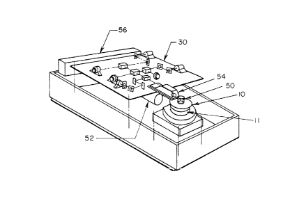
Referring now to Figure 8, there is shown therein a
cutaway pictorial drawing of the optical disk drive system of the
present invention. The drive includes a spindle motor 11 which
drives spindle 50 to which at least one disk 10 is rigidly
mounted. The disk 10 is shown proportionately smaller than it
actually is for purposes of clarity. As discussed herein, the
disk drive system of the present invention has dimensions such
that it fits within a standard slot of a personal computer for
receiving a 5-1/4" Winchester disk drive, floppy drive, or WORM.
The optical disk itself it preferably of diameter of about 130
millimeters with an inside diameter of 40 millimeters, that is,
the same general size as a standard magnetic 5-1/4" hard disk.
The drive also includes an actuator drive motor 52 which is shown
as a linear actuator, for positioning the head 54 over the disk
10. Although the actuator drive motor is shown as a linear
actuator, as is known in the art, a rotary type motor with a
rotary positioning mechanism can alternatively be used.
- 27 -
1333~22
The optical disk drive system of the present invention
has the following specifications:
DRIVE SPECIFICATIONS
Disk
Track number/side 19~700
Track pitch 1.6 micron
Recording material ETOM~
Data transfer rate 200 Mbits/sec.
Storage Capacity 500 MBytes per side
Drive
Rotation method CAV
Disk rotation speed >4000 rpm
Write laser power 0.1 mW
Write laser wavelength 450 nm
Read laser power 0.5 mW
Read laser wavelength 830 nm
Erase Power 2.0 mW
Mass of moving carriage <10 g
- 28 -
1 ~ 3 3 ~ 2 r ~1
System
Disk diameter 130 mm
Data transfer rate >40 Mbits/sec.
Average access time 20 ms
C/N ratio (bandwidth 30kHz) 57dB
Error rate (without ECC) lo~6
Error rate (with ECC) 1o~12
Direct read after write Yes
As described briefly in connection with Figure 7, the
disk drive of the present invention also utilizes an optical
processing unit 30, which will be described in more detail in
connection with Figure 10. An electronics card cage 56 for
supporting electronic circuit boards in a plane parallel to the
optical processing unit may also be included in the construction
of the optical drive system of the present invention. It should
be noted that in order to operate properly, the entire disk drive
system should be enclosed in such a manner that outside light and
contaminating particles cannot reach the surface of the disk.
That practice is commonly used in connection with Winchester disk
drives, as is a particle filtration system which can also
preferably be used with the drive of the present invention.
It should also be noted that although Figure 8 shows an
embodiment of an optical disk drive of the present invention with
a single optical disk, such optical disk drive could be configured
with an additional head in order to utilize the bottom surface of
the disk 10, once it had been appropriately prepared in a manner
as described hereinabove. In a like manner, a plurality of heads
and disks can be utilized in order to increase the storage
- 29 -
1333422
capacity of the optical disk drive system. The disk 10 could also
be coated with additional electron trapping layers to increase its
storage capacity.
The erasable optical disk drive system of the present
invention preferably uses a tracking system similar to or the same
as is currently known and used with WORM drives. An alternative
servo tracking system, designed specifically to operate a rotary
actuator mechanism for use with the present invention, is shown in
Figures 9A and 9B. The circuitry of Figure 9A is a position
tracking servo system which provides track following functions.
The Figure 9B circuitry provides the velocity feedback signals for
track seeking operations.
Referring now to Figure 9A, there is shown a schematic
block diagram of the position tracking servo system for use with a
rotary actuator coarse positioning mechanism together with a
galvanometer-based fine tracking mechanism. The rotary actuator
mechanism, as is known in the disk drive art, works mainly in a
lower frequency range below its resonances while the galvanometer
operates at a higher frequency range. The rotary actuator/
galvanometer system functions as if it were a resonance-free
actuator because the crossover frequency between the two sub-
systems is high enough to neglect the movement of the galvanometer
which is mechanically separated from the rotary arm actuator.
- 30 -
1333~22
The output from the detector D1 of Figure 10 is fed into
a phase compensator 90 of Figure 9A. The output from the phase
compensator 90 is fed to the inputs of both low-pass and high-pass
filters 92 and 94 respectively. The output of the low-pass filter
92 is used to drive the actuator S4a while the high-pass filter 94
output is fed to the galvanometer 96. In a known manner, a
tracking error signal is generated by the operation of the
actuator 54a and galvanometer 96, which is fed back ultimately to
the phase compensator 90. In this manner, the feedback loop of
Figure 9A reduces the off-track errors for the rotary actuator 54a
to the range of tenths of a micron. The galvanometer 96 reduces
that error to a range of hundredths of a micron. Since the
angular range of the galvanometer is in the order of seconds, any
tracking offset caused by beam deflection is negligible.
Figure 9B is a schematic block diagram of the velocity
tracking servo system for use with the present invention. The
track seeking operation is executed under a known velocity-profile
system. A laser beam spot, starting from a track, lands on a
target track after acceleration, constant velocity movement, and,
finally, deceleration. During the deceleration phase, the
velocity is controlled by referring to a distance-velocity table
stored in the ROM 102, which is programmed such that the velocity
of the actuator 54a becomes almost zero at the target track. The
distance between the starting point and the target track is
measured by track-crossing signals and counted by track counter
100. The velocity in the high velocity range is obtained from the
- 31
1333~2-~
time duration of each signal. In the lower velocity range, the
time duration is obtained from the differential of the signal at
each zero-crossing point.
The output from the track counter 100 is inputted to the
ROM 102 whose digital output is converted to a corresponding
analog signal by digital-to-analog converter 104 and fed to a
differential amplifier 106 whose output is fed to both the low and
high pass filters, 92 and 94. The outputs of those filters are
used to drive the actuator 54a and galvanometer 96. The
differential 106 is also connected to receive a signal indicating
whether the actuator is to be driven in either high velocity or
low velocity mode.
Figure 10 is a block diagram of a preferred embodiment of
the optical processing unit 30. Also shown is the actuator
assembly 54. The modulated beam of the write laser 28 is
reflected from a first broad band mirror M1 to a second broad band
mirror M2 and then passes through two lenses L1 and L2 until it
reaches an element of a polarizing beam splitter PBS2 which
preferably provides as an output a laser beam with peaks at a
wavelength of about 450 nanometers. PBS2 is preferably a 488 nm
polarizing beam splitter cube, model no. 03PBS 013, available from
Melles Griot Corporation. Lens Ll is preferably a 50 millimeter
precision optimized achromatic doublet lens while lens L2 is
preferably a 200 millimeter precision optimized achromatic doublet
lens, both available from Melles Griot Corporation. After being
- 32 -
133`~22
reflected by the polarizing beam splitter PBS2, the write laser
beam passes through mirror M8, which is an 850 nm reflector, and
then through mirror M9, which is preferably a 650 nanometer
wavelength reflector mirror, and onto lens L6 which is an Olympus
'TAHOS' autofocusing objective as discussed above. The 450 nm
write beam is then reflected by broad band mirror M7 and
translated 90 to impinge onto the surface of the optical disk 10.
The lens L6 and broad band mirror M7 are contained on the actuator
assembly 54 which includes an actuator arm assembly and head.
The 650 nm reflector Mg may preferably be a 6328
dielectric reflector, model no. 02 MFG007/279, available from
Melles Griot Corporation. It functions to reflect only
wavelengths which peak around 650 nm, such as the orange light or
data given off by the electron trapping layer 16 of the disk 10 in
response to the read laser beam. The mirror M7, which reflects
the incident write and read laser beams to focus on the lens L6
into a path 90 away from the incoming beams, is preferably a
broad band reflector, model no. lODlOBD-l, available from Newport
Corporation. Mirrors Ml and M2 may preferably also be the same
mirror as mirror M7. Mirror M7 also functions to reflect into a
path 90 away from the incoming path the data stored on the disk
in its orange light form and focused onto the mirror M7 by the
lens L6. Such "light beam" is really a stream of orange light or
"bits" read from the disk 10. The actuator arm assembly may be of
any known construction. Suitable such assemblies are utilized in
well known WORM drives.
- 33 -
1333~
The read/focus laser 38, which preferably has its peak
wavelength in the infrared range centered around a wavelength of
1,000 nanometers, is first reflected 90 by a broad band mirror M4
and then another 90 by a second broad band mirror M5 which
directs the read/focus laser beam to the back of a polarized beam
splitter PBSl having a wavelength centered about 830 nanometers.
The read/focus beam, which is polarized in a plane parallel to the
surface of the drawing, passes through the polarized beam splitter
PBSl and through a quarter wave plate ~4, which may preferably be
a model no. 02URQ001 available from Melles Griot Corporation. The
quarter wave plate changes the polarization of the read beam to
circular polarization. The read beam then impinges on an 850 nm
reflector mirror M8, which bends the beam 90 to impinge on the
650 nm dielectric reflector mirror Mg. The read/focus beam passes
through the mirror Mg in the same manner as the write laser beam
and impinges onto the lens and mirror combination L6 and M7 of the
head 32 secured to the actuator assembly 54 which focuses it onto
the surface of the disk 10.
A portion of the read/focus beam is reflected off of the
surface of the disk 10, through the objective formed by lens L6
and mirror M7 and through mirror Mg to mirror M8. Due to its
reflection off of the disk 10 surface, the polarization of the
focus beam is now in the opposite circular direction to the
circular polarization of the read/focus beam. The focus beam is
reflected 90 by the mirror M8 and through the quarter wave plate
- 34 -
1333422
, which changes its polarization to vertical or perpendicular to
the surface of the drawing. It then impinges onto the front of
the polarized beam splitter PBSl, which may preferably be a 830 nm
polarized beam splitter tube, model no. U3 PBS063, available from
Melles Griot Corporation. The beam splitter PBS1 reflects the
focus beam at an angle 90 to the incident beam which causes the
focus beam to impinge on mirror M5, which may preferably be a
diode laser reflector, model no. 10 DIOBD-2, available from
Newport Corporation. Mirrors M3 and M4 may preferably be that
same part.
The mirror M5 reflects the focus beam at an additional
90~ angle such that it is on a path parallel to, but travelling in
opposite direction to, the output laser beam from the read/focus
laser 38. The focus beam is reflected by mirror M5 onto and
focused through a first lens L3, which may preferably be a 75
millimeter precision optimized achromatic doublet lens and then
through a second lens L4 which may preferably be a 50 millimeter
plano convex cylinder lens model no. 850-50, available from optics
Plus, Inc., and onto a focus/tracking detector D1. Such detector
D1 forms a part of element 40 in Figure 7 and may preferably be a
quadrant detector, model PIN-SPOT-40MI, available from United
Detector Technology Corporation. The output from detector Dl is
utilized by the detector assembly 40 to produce a feedback signal
for use by the focus electronics 34 for maintaining the focus of
the read and write laser beams by the head 32, as well as
providing an input to the detector electronics 42. The hard
- 35 -
133342~
mounted optical system 31 is formed of the optical elements shown
in Figure 10, excluding elements 28, 38, Dl, D2 and the actuator
assembly 54 in its entirety.
The photons released by the impingement of the read beam
onto the surface of the disk 10 pass through the lens L6 and are
bent by the mirror M7 and caused to impinge on the backside of the
reflector Mg. The reflector Mg translates the outgoing data beam
90 away from the input beam and directs it through a lens L5,
which may preferably be a 120 millimeter focal length precision
optimized achromatic doublet lens available from Melles Griot
Corporation. From the lens L5, the data beam impinges on a cold
mirror M6 which translates it 90 to pass through an optional 650
nm interference filter f1 to impinge onto a data read detector D2.
The data read detector D2 forms a part of the detector assembly 40
described in connection with Figure 7. The cold mirror M6 may
preferably be a model no. 03MCS007, available from Melles Griot
Corporation.
Although only a preferred embodiment is specifically
illustrated and described herein, it will be appreciated that many
modifications and variations of the present invention are possible
in light of the above teachings and within the purview of the
appended claims without departing from the spirit and intended
scope of the invention.
- 36 -