Note: Descriptions are shown in the official language in which they were submitted.
1 33384~
IMPROVED MULTICHANNEL GAS ANALYZER
AND METHOD OF USE
. ._
Technical Field
The present invention relates to systems
for measuring the partial pressures of constituent
gases in a gas stream. More specifically, the in-
vention relates to improved multichannel gas analyzer
systems used to measure the partial pressures of
constituent gases in respiratory gas streams and
display representative gas data information on a CRT
display.
Background
During surgery, anesthetized patients are
almost universally intubated. Measurement of respi-
ratory gases is desirable when a patient is mechani-
cally intubated through an endo-tracheal tube. An
analysis of the inhaled and exhaled gas mixture pro-
vides information about the patient's ventilation.
These observations can prevent the patient's receipt
of excessive amounts of anesthetic.
Carbon dioxide ~C02), nitrous oxide (N20)
and the anesthetic agent are the constituent gases
of most interest in measuring respiratory gas streams.
It is well known that C02 in the bloodstream
equilibrates rapidly with C02 in the lungs. Hence,
the partial pressure of the C02 in the lungs
-2- 1 333849
approaches the amount in the blood during each breath.
Accordingly, the C02 content at breath's end, termed
end-tidal C02, is a good indication of the blood
C2 level.
Abnormally high end-tidal C02 values
indicate that an insufficient amount of C02 is being
transported away from the bloodstream through the
lungs, i.e., inadequate ventilation. Conversely,
abnormally low end-tidal C02 values indicate poor
blood flow to the tissues, inadequate C02 transport
through the lungs, or excessive ventilation.
Mass spectrometers are used for measuring
the partial pressure of respiratory gases in, for
example, operating room suites in which one spectro-
meter is shared by many rooms. Mass spectrometers
have the advantage of measuring a multiplicity of
gases; however, the disadvantages are their cost,
- maintenance and calibration requirements, slow
response time, and noncontinuous measurement.
Gas analyzers using non-dispersive infrared
spectrophotometry are also used for partial pressure
gas measurement. While these analyzers are less
expensive than mass spectrometers and continuously
measure partial gas pressure, their disadvantages
are poor response time and difficulty in calibration.
Prior art non-dispersive infrared gas
analyzers include features for making C02 and N20
cross channel detection, temperature, and collision
broadening corrections to their partial gas pressure
measurements. Some of these corrections are made
automatically by the analyzers while others are made
manually by the operator.
Non-dispersive infrared gas analyzers gener-
ally have two configurations. The first, and most
common, is the sampling or side-stream type. This
type diverts a portion of the patient's respiratory
gas flow through a sample tube to the infrared analyzer.
_3_ 1 333~49
The second type mounts on the patient's
airway and uses a portion of the airway as the sample
chamber. This type is frequently occluded by the
mucus and moisture in the patient's airway and its
bulk on the airway can affect the patient's breathing.
Both infrared gas analyzer configurations
are characterized by small absorption levels by the
constituent gases which lead to small signals and
stability problems.
Increasing the analyzer's sample chamber
size improves the small signal and stability problems;
however, it increases the response time. Increasing
the gas flow rate through the analyzer improves the
response time, but occlusions are more frequent and
the patient's normal ventilation volume is impaired.
In this regard, neonates require sample
flow rates equal to or less than 50 cc/minute.
However, neonates also require the analyzer's response
time to be compatible with breath rates well in excess
of 60 breaths per minute. This condition equates to
a response time of less than 100 milliseconds.
Another disadvantage of infrared gas
analyzers is that they require frequent calibration
for proper operation. Factors affecting calibration
of the optical bench portion of a gas analyzer include
manufacturing tolerances relating to the sample cell
dimensions (particularly thickness); brightness of
the infrared source and sensitivity of the photo-
detectors; temperature; barometric pressure; and the
accumulation of dirt or moisture in the optical
bench's gas pathways.
Changes in the optics and electronic cir-
cuitry over time require recalibration of infrared
gas analyzers. Careful construction of the optics
and electronic circuitry minimizes the number of
calibration adjustments needed and the period between
recalibration. Hence, interchangeability of the
1 ~3~
--4--
optical bench of an analyzer has not heretofore been
practical because of the need for recalibration when
the optical bench is connected to the analyzer.
Calibration of infrared gas analyzers is
accomplished by various electronic circuit adjust-
ments to correct for variations in sample chamber
geometry as well as variations and drift of various
sensing components.
Calibration usually requires taking the
analyzer out of service and passing standard gases
through it, in the presence of which the various
adjustments are made. Another calibration method is
to make a "zero gas" reading for the optical bench
and adjust the analyzer's amplifier so that the
analyzer's output actually reads zero. A still
further method uses a reference cell filled with a
non-absorbing gas or a reference filter having a
wavelength at which no absorption takes place to
stabilize the zero setting of the analyzer.
Prior art non-dispersive infrared gas
analyzers also include some automatic calibration
features. However, further operator controlled
calibration procedures are required before the
analyzers are ready for use.
The present invention overcomes these and
other problems of prior infrared gas analyzers as
will be set forth in the remainder of the specifica-
tion.
Summary of the Invention
The present invention is an improved non-
dispersive infrared gas analyzer system for analyzing
respiratory gas streams and displaying information
about the detected constituent gases. The system
has an optical bench with associated circuitry. The
circuitry generates signals representative of the
partial pressures of C02, N20 and the anesthetic
-5- 1 3 3 3 8 4 q
agent present in a gas stream; the temperature within
the optical bench; the flow rate of the gas stream
through the optical bench; and the pressure within
the optical bench's gas pathway. The system pump
draws respiratory gases through the optical bench's
gas pathway and backflushes this same pathway. Analog
input circuitry is electrically connected to the
optical bench and receives the optical bench's signal
outputs indicative of certain measured values and
characterization information. The analog input cir-
cuitry processes the input signals and outputs them
to the analog processing circuitry. The analog pro-
cessing circuitry, which includes a microprocessor,
performs calculating functions on the received signals.
The results are output signals indicative of the
partial pressure of C02, N20 and the anesthetic agent
corrected for temperature, barometric pressure, col-
lision broadening, cross-correction and characteri-
zation. These signals along with those for the mea-
sured values of flow rate, temperature and pressurewithin the optical bench are output to the display
section of the system.
The display section circuitry, according to
its programming, processes the signals output from the
analog processor circuitry. The output signals from
the display section circuitry drive a CRT for display
of graphics and characters representative of measured
values from the optical bench.
The optical bench circuitry preliminarily
processes the signals output from the gas and other
detectors such as an absolute-reading pressure sensor
for pressure measurement, a differential-reading
pressure sensor for measuring flow rate, and a tem-
perature sensing circuit.
The optical bench has three optical detec-
tion assemblies for simultaneously measuring C02,
N20 and a volatile halogenated hydrocarbon anesthetic
1 33384q
_ -6-
(or agent). The bench continuously measures these
gases at a rate which allows separate analysis of
the inspired and expired gas mixtures.
Preferably, the three optical detection
assemblies and the connected detection circuitry are
incorporated in a small optical bench that is placed
next to the patient. The optical bench connects to
a larger apparatus constituting the remainder of the
gas analyzer system.
A small diameter sample tube, preferably
one yard long or less, connects the optical bench to
a side-stream type airway adaptor. A filter in the
airway adaptor blocks liquids, such as water and
mucus, from entering the sample tube and optical
bench. The walls of the sample tube absorb water
vapor condensing on them and evaporate it into the
atmosphere. An optical bench entrance filter filters
any remaining water vapor and dirt in the gas stream
from entering the optical bench.
A system pump contained in a pump assembly
draws a continuous stream of respiratory gas through
the gas pathway of the optical bench. This pump
also backflushes the gas pathway. A flow shaper at
the entrance of the optical bench reshapes the gas
flow cross-section from round to rectangular. The
gas stream passes through the C02, N20 and agent
detection channel assemblies in succession as it
transits the gas pathway.
The C02 and N20 detection channel assemblies
are disposed along the portion of the gas pathway
having a rectangular cross-sectional shape. The
agent detection channel assembly is located in another~
portion of the gas pathway having a cylindrical shape.
After leaving the portion of the gas pathway
containing the agent channel, the gas stream enters the
area in the gas pathway containing a pressure sensor
and a flow rate sensor. The gas stream then leaves
_7_ 1 33384~
the optical bench, enters a scavenging tube and is
exhausted from the system through the pump assembly.
The C02 and N20 detection channel assemblies
each use a small section of the gas pathway with the
rectangular cross-section. A sapphire window replaces
a part of the gas pathway wall. An infrared source
is located behind the window. A narrow-band infrared
filter replaces a part of the gas pathway wall opposite
the sapphire window. An infrared detector for each
channel aligns with the respective optical paths
behind the filter.
The agent detection channel assembly is in
the portion of the gas pathway with a cylindrical
shape. An infrared source is located at one end of
the cylindrical section and a narrow-band filter
closes the opposite end. The infrared detector
aligns with the optical path behind the filter.
A chopper wheel, common to the three
ch~nnels, rotates in a plane between the detectors
and associated narrow-band filters. The chopper
wheel chops the infrared light passing through the
filters at a predetermined frequency.
The optical bench also includes an electric-
ally erasable programmable read-only memory (EEPROM)
which stores characterization information for the
specific optical bench. The characterization infor-
mation corrects the optical bench's measurements for
system component performance that deviates from ideal
theoretical performance. The characterization infor-
mation obviates the need to calibrate the opticalbench. Characterization information includes coeffi-
cients for temperature, collision broadening, cross
correction, span, offset, and pressure. Characteri-
zation information also includes coefficients for
detector sensitivity changes for changes in the
detected DC voltage. The characterization infor-
mation is used by the analog processor circuitry and
1 ~ 3 ~
- -8-
the display circuitry in carrying out their signal
processing functions.
The analog input circuitry and the analog
processor circuitry process the analog signals gen-
erated by the optical bench circuitry. The processedsignals, now digital, are output by the analog pro-
cessor circuitry and transmitted to the display
section. The display section processes the signals
for display on a CRT.
The main display section circuits are
the display processor circuitry and pixel circuitry.
The display processor circuitry bidirection-
ally communicates with the analog processor circuitry.
The display processor circuitry controls the pixel
circuitry. This control results in driving the CRT
to display both the fixed characters and scrolled
information, e.g., a capnogram.
Preferably, the CRT displays numerical and
graphical data. The numerical data normally displayed
are the inspired and expired values for C02, N20, and
anesthetic agent, and respiration rate. The graphical
data normally displayed are the waveforms for C02
and N20. These waveforms are an indication of the
patient's respiratory cycle. Superimposed on, for
example, the C02 waveform are the transition points
between inspiration and expiration, and between expi-
ation and inspiration. These points are marked with
an "I" and an "E", respectively. The "I" and "E"
markings provide the physician with the locations of
selected transition points in both normal and abnormal
capnograms.
An object of the present invention is to
provide an apparatus and method for improved measure-
ment of the partial pressure of respiratory gases.
Another object of the present invention is
to provide an improved apparatus and method for
measurement of the partial pressure of respiratory
9 1 33384~
gases with a rapid response time of less than 100
milliseconds and a sample flow rate less than or
equal to S0 cc/min.
A further object of the present invention
is to provide an apparatus capable of self character-
ization without calibration.
A still further object of the invention
is to provide an improved apparatus which does not
require the use of a reference channel for stabilized
operations.
An even further object of the present
invention is to provide an improved apparatus in
which the optical bench portion of a gas analyzer
can be interchanged without the need to recalibrate
lS the system before use.
Another object of the present invention is
to provide a system for displaying the gas concentra-
tions of a patient's respiratory gas stream, scrolling
waveforms across the display screen and marking
inspired and expired transition points of a patient's
breathing cycle.
These and other objects of the invention
will be described more fully in the remaining portions
of the specification.
Brief Description of the Drawings
Figure 1 is a block diagram of the multi-
channel gas analyzer system of the present invention.
Figure 2A is an exploded view of the optical
bench portion of the multichannel gas analyzer of
the system of the present invention.
Figure 2B shows the three optical detection
channels, with the detection assembly equipment shown
in an exploded view.
Figure 2C shows the C02/N20 detection
channel assembly of the optical bench shown in
Figure 2.
,, -10- 1 3 3 3 3 4 q
Figure 2D shows the agent detection channel
assembly of the optical bench shown in Figure 2.
Figure 3 is a block diagram of the pump
assembly of the gas analyzer system of the present
invention.
Figure 4A is a schematic diagram of the
circuitry of the optical bench of the multichannel
gas analyzer system of the present invention.
Figure 4B is a schematic diagram of the
AC/DC separation circuit in the amplifiers that
receive the signals output from the three infrared
detectors shown in Figure 4A.
Figure 5 is a schematic diagram of the
analog input circuitry of the multichannel gas
analyzer of the present invention.
Figures 6A, 6B, and 6C comprise a schematic
diagram of the analog processor circuitry of the
multichannel gas analyzer system of the present invention.
Figure 7A is a schematic diagram of the circuitry on
the motherboard of the multi-channel gas analyzer system of
the present invention.
Figures 7B, 7C and 7D show signals which transmit
the motherboard without being processed by the circuitry.
Figure 8 is a schematic diagram of the
display processor circuitry of the multichannel gas
analyzer system of the present invention.
Figures 9A, 9B and 9C comprise a schematic
diagram of the pixel circuitry of the multichannel
gas analyzer system of the present invention.
Figures lOA, lOB and lOC comprise a sche-
matic diagram of the scroll/pixel gate array of the
pixel circuitry shown in Figure 9B.
Figure ll is a schematic diagram of the
CRT memory control gate array of the pixel circuitry
shown in Figure 9B.
Figure 12 is a schematic diagram of the
digital output section of the display section of the
~1
-- -11- 1 333849
multichannel gas analyzer system of the present
invention.
Figure 13 is a schematic diagram of the
system controls and alarms for the multichannel gas
analyzer system of the present invention.
Figure 14 is a block diagram of the software
for controlling the multichannel gas analyzer system
of the present invention.
Figure 15 shows a representative CRT screen
display for the multichannel gas analyzer system of
the present invention.
Detailed Description of
the Preferred Embodiments
The present invention is an improved multi-
15 channel gas analyzer system for measuring the partial
pressure of constituent gases of a respiratory gas
stream. The analyzer system also displays numerical
and graphical information about the constituent gases
detected.
The figures refer to electronic components
or circuitry that consists of a group of components
which carry out a known specific function. Those
components or circuit elements that are well known
by those skilled in the art will be referred to
generally by their common names or functions and are
not explained in detail.
Figure 1 is a schematic diagram of the
multichannel gas analyzer system of the present
invention. The system comprises an analog section
102 and a display section 104. Analog section 102
detects and measures the constituent gases of a
respiratory gas stream. This section also detects
and measures other physical properties which affect
the determination of the partial pressures of the
constituent gases, i.e., C02, N20 and the agent-
The measured values for C02, N20, the agent and the
- -12- 1 3 3 3 8 4 q
other physical properties are combined to calculate
the "real" partial pressure of each constituent gas.
The "real" partial pressures of the constituent gases
are corrected for barometric pressure, temperature,
S collision broadening, channel cross-detection, sen-
sitivity changes in the detection devices, and char-
acterization of the detection circuitry and other
detection components.
The calculated values for the partial
pressure of C02, N20 and the agent are output from
analog section 102 in digital form to display
section 104. Analog section 102 also transmits
measured values for flow rate, temperature, and
pressure to the display section.
Display section 104 processes the analog
section output signals. The C02, N20 and the agent
output signals are processed for display on the CRT
as numeric characters. The display section also
processes at least the C02 signals for graphic dis-
play as, for example, a scrolling capnogram. The
display section processes the temperature, pressure
and flow rate signals for display and as historical
data for later retrieval.
The display section has system controls
for operator interface. These controls select system
operation and choice of screen displays. The dis-
play section also has both digital and analog out-
put ports for communicating with peripheral equip-
ment. The display section includes visual and
audible alarms to indicate alarm conditions or
improper operation of the system.
Analog section 102 comprises optical bench
109 (whose electronics include detector circuitry 110
and preamp 118); pump assembly 112; analog input
circuitry 122 and analog processing circuitry 124.
Patient adaptor 106 and sample tube 108 are not part
of analog section 102. Patient adaptor 106 is a
- -13- 1 3 3 3 8 4 q
conventional side-stream type and filters the gas
stream drawn toward optical bench 109 by pump assembly
112.
Sample tube 108 connects patient adaptor
106 to optical bench 109. The walls of sample tube
108, preferably constructed of Nafion, absorb and
then evaporate condensed water vapor within the tube.
Nafion is commercially available from E.I. du Pont
de Nemours and Company, Wilmington, Delaware. (Nafion
is a trademark of E.I. du Pont de Nemours and Company,
Wilmington, Delaware.)
Measurement accuracy increases the closer
to the patient gas detection is made. For this reason,
optical bench 109 is small and placed close through
the intubated patient. The length of sample tube 108
is preferably one yard or less.
Display section 104 is described generally
and in detail in discussing Figures 7 through 13.
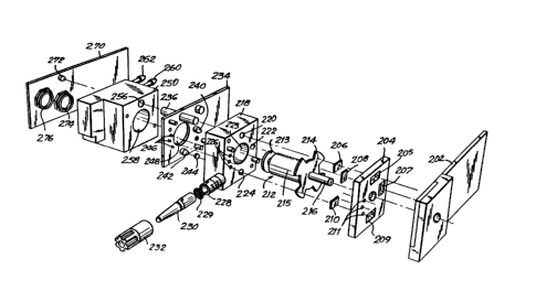
Figures 2A-2D show optical bench 109. End
cap 202 (Figure 2A) forms the top of the optical
bench. The hole through the center receives the end
of stator shaft 216.
Detector block 204 is fixed to the inwardly
directed surface of end cap 202. Detector block 204
has openings 205, 207 and 209. Infrared photo-
detectors 206, 208 and 210 are fixed in openings 205,
207 and 209, respectively. Detectors 206, 208 and
210 detect the amount of infrared light illuminating
them from their optical paths. The trio of small
holes, indicated generally at 211, have photodiodes
fixed in them. Each photodiode is in an optical
path with one of the LED's indicated generally at 246
mounted on lamp board 234. The three LED/photodiode
pairs determine and maintain a constant chopping
frequency. Detector block 204 also has an opening
that receives stator shaft 216.
-14- 1 333849
The chopper assembly 212 includes rotor 215,
end shield 213, chopper wheel 214 fixed to the end
of rotor 215 and a stator of which only stator shaft
216 is shown. The three LED/photodiode pairs accom-
plish motor speed control as will be discussed.
Block 218 contains gas inlet 228, first
gas passageway 302 (Figure 2B) and openings 220, 222
and 224 for receiving optical filters 308, 306 and
304 (Figure 2B), respectively. Openings 222 and 224
do not extend through block 218. Another opening of
a predetermined depth and aligned with each opening
is formed in the opposite side of block 218 (not
shown). These openings receive sapphire windows 238
and 244 (Figure 2B) for the N20 and C02 detection
channels, respectively.
Three bores, indicated generally at 226,
extend through block 218. These bores are part of
the optical paths for the three LED/photodiode pairs.
Central opening 223 in block 218 receives motor 212.
Associated with block 218 are flow shaper
230, in-line filter 229 and lock nut 232. Flow
shaper 230, in-line filter 229 and lock nut 232 con-
nect sample tube 108 to optical bench 109.
Lamp board 234 has infrared lamps 240 and
242, and the three LEDs indicated at 246 mounted on
one side. Agent channel 236 is shown disposed through
lamp board 234. Agent channel 236, shown as a cylin-
drical tube, has a portion received by block 218 and
a portion received by block 250, as is better shown
in Figure 2D.
When the optical bench is assembled, lamps
240 and 242 fit in the openings aligned with open-
ings 222 and 224 in the opposite side of block 218,
as is best shown in Eigure 2C. The three LEDs fit
in the bores indicated at 226 in block 218. Lamp
board 234 has opening 248 that receives chopper
motor 212.
-15- 1 333849
Block 250 contains two cavities in its
bottom surface. The first cavity receives pressure
sensor 274 mounted on pressure sensor board 270; and
the second cavity receives flow rate sensor 276
mounted on the same board. Gas passageway 376 con-
nects the first cavity to agent channel 236. The
first and second cavities are in fluid comminication
via the restriction at 277 (Figure 4A). Block 250
has gas outlet fitting 260 and backflush inlet fit-
ting 262. Both the gas outlet and backflush inlet
fittings are in fluid communication with the second
cavity in the bottom of block 250. Opening 258
receives chopper motor 212.
Pressure board 270 forms the bottom of the
optical bench. Pressure sensors 274 and 276, and
infrared lamp 272 are mounted on this board. Pres-
sure sensor 274 is configured to measure pressure.
Pressure sensor 276 is configured to measure flow
rate as will be explained.
When assembled, infrared lamp 272 seats in
the end of agent channel 236, as is best shown in
Figure 2D.
Figure 2B shows the gas passageways that
are used for the C02, N20 and agent detection
channels. This Figure shows infrared lamps 242, 240
and 272; sapphire windows 244 and 238 (C02, N20
channels only), optical filters 304, 306 and 308;
chopper wheel 214; and detectors 210, 208, and
206. These elements are combined to form the three
detection channel assemblies as will be discussed in
describing Figures 2C and 2D.
Preferably, infrared sources 240, 242 and
272 are subminiature lamps manufactured by Gilway
Company, Woburn, Massachusetts.
Optical filter 304 has a center wavelength
of 4.265 microns and a bandwidth of 2.25%. This
coincides with the absorption band of C02. Optical
-- -16- 1 333849
filter 306 has a center wavelength of 4.508 microns
with a bandwidth of 2.35%. This coincides with the
absorption band of N20. Optical filter 308 has a
center wavelength of 3.310 microns with a bandwidth
of 1%. This coincides with the absorption bands
common to the three agent gases. These filters are
commercially available from Optical Coating
Laboratory, Inc., Santa Rosa, California.
Detectors 206, 208 and 210 are lead selen-
ide infrared detectors. Preferably, the detectorshave a 3 mm square active area and are manufactured
by Optoelectronics, Inc., Petaluma, California.
Again referring to Figure 2B, the respira-
tory gas stream enters the optical bench through
flow shaper 230. In-line filter 229, preferably
constructed of expanded PTFE with a 1 micron pore
size, is disposed across the inlet passageway. The
filter stops any foreign material from entering the
optical bench. The entering gas flow has a circular
cross-sectional shape. Flow shaper 230 and the in-
line filter reshape the flow to the rectangular cross-
sectional shape of gas passageway 302 without form-
ing eddies. However, other configurations for the
inlet to accomplish flow shaping without a filter
may be used.
The arced shape of gas passageway 302
accommodates using chopper wheel 214 for signal
chopping. If other chopping methods are used, this
passageway may have other shapes.
Figure 2C depicts the C02 and N20 detec-
tion channel assemblies. The reference numbers in
Figure 2C are for the C02 detection channel. The
C2 and N20 detection channel assemblies are iden-
tical. Hence, in describing Figure 2C, the N20
detection channel component reference numbers will
follow in parentheses those for the C02 detection
channel.
_ -17- 1 33384 9
C2 channel detector 210 (208) is fixed to
one side of detector block 204. Optical filter 304
(306) for the C02 channel is fixed in opening 224 (222)
of block 218. Optical filter 304 (306) forms part
of the sidewall of gas passageway 302. Opening 301
is bored in the opposite side of block 218. Sapphire
window 244 (238) is disposed in opening 301 and forms
the side wall of gas passageway 302 opposite that
formed by optical filter 304 (306). When lamp
board 234 is fixed to block 218, infrared lamp 242
(240) is disposed in opening 301 behind sapphire
window 244 (238).
Chopper wheel 214 rotates between detector
210 (208) and optical filter 304 (306). The openings
in chopper wheel 214 are aligned with and common to
the three optical paths. Chopping results in the
generation of square wave signals indicative of the
uncorrected partial pressures of C02, N20 and agent
in the gas stream.
Figure 2D shows the agent detection channel
assembly.
Detector 206 is mounted on one side of
detector block 204. Optical filter is fixed in
opening 220 in block 218. Optical filter 308 forms
one end of the agent optical channel 236. Infrared
lamp 272 is mounted on pressure board 270. When the
optical bench is assembled, lamp 272 ingresses and
closes the other end of the agent optical channel.
Gas passageway 376 in block 250 is the gas passage-
way to the cavities containing pressure and flowsensors 274 and 276, (Figure 2A).
Preferably, the optical path length of
passageway 302, as part of the C02 and N20 detector
channels, is 0.1 inches; and the optical path length
of agent detector channel 236 is 1 inch. The agent
optical path length is longer because agents, such
-18- 1 33384~
as halothane, ethrane and forane, are weaker absorb-
ers than C02 and N20.
Figure 3 discloses the pump assembly shown
in Figure 1 at 112. The pump assembly's purpose is
to draw a respiratory gas stream through the gas
pathway at the preferred rate of 50 cc/min. and
backflush the system.
Vacuum suction line 114 is connected to
inlet fitting 404. Internal passageway 422 connects
inlet 404 to "zero" valve 406. Internal passageway 408
connects room air inlet filter 420 and "zero" valve
406. ZER0+ line 410 and ZER0- line 412 are the power
lines for "zero" valve 406. The voltage across these
lines determines which incoming passageway to "zero"
valve 406 is selected.
Internal passageway 424 connects "zero"
valve 406 to vacuum pump 414. The power lines to
pump 414 are AIRPUMP+ line 416 and AIRPUMP- line
418. The voltage across these lines controls the
speed of the pump.
Internal passage 426 connects vacuum pump
414 to backflush valve 428. The power lines to back-
flush valve 428 are BACKFLUSH+ line 430 and BACK-
FLUSH- line 432. The voltage across these lines
determines which outlet passageway is selected by
the valve.
The first outlet of backflush valve 428 is
internal passageway 434. It connects backflush
valve 428 to exhaust port 436. The other outlet is
internal passageway 438. It connects backflush
valve 428 to backflush line 116 to the optical bench
via C02 scrubber 440. The C02 scrubber prevents,
for example, any exhaled C02 from the operator from
entering the optical bench during backflush. The
timing of the selection of each output line will be
discussed subsequently.
-19- 1 333~4q
During normal operation, "zero" valve 406
is powered to select inlet passageway 422 containing
the respiratory gas stream. Backflush valve 428
under these conditions is powered to select outlet
passageway 434 that connects to exhaust port 436.
Periodically, the optical bench is back-
flushed to make a zero gas reading, determine the
barometric pressure at the optical bench's location
and clean filter 229 (Figure 2B), as well as the
patient adaptor filter (Figure 1). To backflush,
the voltage across the power lines to "zero" valve
406 and backflush valve 428 is changed. "Zero"
valve 406 is powered to select internal passage-
way 408 containing room air. Backflush valve 428 is
powered to select outlet passageway 438 that connects
to backflush line 116 via C02 scrubber 440. The
voltage across the power lines to vacuum pump 414 is
changed as necessary to clean the filters.
Figure 4A is a schematic diagram of the
circuitry and selected components of optical bench
109. The gas stream enters passageway 302 in optical
bench 109 traveling in direction A. The gas stream
first travels past the C02 detection channel assembly
comprising infrared light source 242, sapphire window
244, optical filter 304 and lead selenide detector 210.
Second, it passes the N20 detection channel assembly
comprising infrared light source 240, sapphire window
238, optical filter 306 and lead selenide detector
208. The gas stream leaves passageway 302 and enters
agent detection channel 236. The agent detection
channel assembly comprises infrared light source
272, optical filter 308 and lead selenide detector
206. Chopper wheel 214, common to all detection
channel assemblies, has openings which allow simul-
taneous detection on all channels.
Broad band optical energy from each infra-
red source is passed through the gas stream. The
~ -20- 1 33384~
filters only pass a narrow infrared band associated
with the absorption characteristics of the specific
gas. The energy streams exiting the filters are
chopped and fall on the seperate detectors. Chopping
forms a square wave output signal from each detector.
The amplitude of the respective signals is indicative
of the amount of energy within the filter's band
transmitted through the gas stream.
The output signal from C02 detector 210
is input to amplifier 470. The outputs of ampli-
fier 470 are the AC component of the C02 signal on
line 471 and the DC component of the C02 signal on
line 211. The output signal from N20 detector 208
is input to amplifier 478. The outputs of amplifier
478 are the AC component of the N20 signal on line
479 and the DC component of the N20 signal on line
209. The signal output from agent detector 206 is
input to amplifier 480. The outputs of amplifier 480
are the AC component of the agent signal on line 481
and the DC component of the agent signal on line 207.
The circuit for separating the AC and DC components
of the signals is shown in Figure 4B.
The three LEDs, indicated generally at
246, and the three photodiodes, indicated generally
at 456, detect the chopper motor ~ position. One
LED/photodiode pair is for the A ~, a second pair
is for the B ~ and a third pair is for the C ~.
These signals are used for insuring that the brush-
less motor is rotating chopper wheel 214 at the
proper speed.
The three photodiodes detect the chopped
light from the LEDs. The output of each photodiode
is a "clean" square wave signal. The three photo-
diode output signals, when combined, approximate
a standard three-phase signal.
The detected signals are output on lines
460, 462 and 464. The signal on line 460 is input
- -21- l 3 3 3 8 4 q
to amplifier 472, the signal on line 462 is input to
amplifier 474 and the signal on line 464 is input to
amplifier 476. These amplified signals are input to
comparators 486, 488, 490, respectively. The compari-
son signal for each comparator is a +5V referencevoltage.
The three comparator outputs are input to
to 3~ brushless motor commutator 498. The outputs
of commutator 498 are input to driver 500. The motor
drive voltage on line 501 is also input to driver 500.
The outputs of driver 500 are the ~A signal on line
502, the ~B signal on line 504 and the ~C signal on
line 506 which drive chopper motor 508 appropriately.
Prior to amplification of the detected ~B
signal from the center LED/photodiode pair, a branch
line inputs the signal to amplifier 484. The ampli-
fier output signal is the GAS SYNC signal on line 485.
The GAS SYNC signal synchronously demodulates the
C02, N2O and agent signals, as will be discussed.
After the gas stream leaves agent channel
236, it enters passageway 376. This passageway
connects agent channel 236 to the first cavity in
the bottom of block 250. This cavity contains pres-
sure sensor 274. The first and second cavities are
connected by the restriction at 277 (Figure 4A). A
passageway (not shown) connects the second cavity to
the gas outlet and the backflush lines.
At this point, the only signals discussed
which are ready for output from the optical bench
are the detected CO2, N2O and agent signals. The
remainder of the signals output from the optical
bench are multiplexed by multiplexer 532 and then
output from the optical bench.
The first input to multiplexer 532 is the
output of EEPROM 530. EEPROM 530 stores coefficients
relating to characterization of the optical bench
and the preferred bench temperature.
1 333849
-22-
The characterization coefficients do not
adjust or change the operation of any component of
the optical bench or the bench as a whole. These
coefficients correct the bench's measurements for
system component deviation from ideal.
The inputs to EEPROM 530 are the data bus
Dl signal on line 542, the SK (serial data clock)
signal on line 540 and the CS (chip select) signal
on line 538. The CS and SK signals control the
EEPROM's output. The Dl signal is the data input to
the EEPROM. All of these signals are output from
quad. flip flop 544. The data inputs to quad. flip
flip 544 are the D0-D3 signals on lines 552, 550,
548 and 546, respectively. The D0-D3 bar signals
are outputs of line driver 554 whose inputs are the
4 bit parallel PRED0-PRED3 bar signals on lines 556,
558, 560 and 562. These signals are from the analog
input circuitry. (The "bar" designation after a
signal name indicates the inverted state of the signal
without the bar designation, as is known by those
skilled in the art).
Quad. flip flop 544 is clocked by the output
of demultiplexer 578. The inputs to demultiplexer 578
are the A0 signal on line 572, the BUS STROBE signal
on line 574 and the Al signal on line 576. These
signals are output from line driver 570. The inputs
to line driver 570 are the PREAl signal on line 564,
PREA~ signal on line 566 and the PRESTRB signal on
line 568. These signals are received from the analog
input circuitry.
The output of demultiplexer 578 depends on
the state of the BUS STROBE signal on line 574.
When properly instructed, the EEPROM out-
puts the characterization coefficients to multi-
plexer 532 as the first input.
The second input to multiplexer 532 is theamplified OB TEMP (optical bench temperature) signal
1 333849
-23-
on line 524. This signal is output from temperature
sensing and control circuit 514. The fifth signal
input to multiplexer 532 is the HEATER DRIVER V
(heater driver voltage) signal on line 523 that is
also output from temperature sensing and control
circuit 514. The optical bench incorporates heating
resistors 510 and 512.
The heating resistors are controlled by
temperature control and sensing circuit 514. In
operation, the optical bench temperature is sensed
and its deviation from the preferred bench tempera-
ture is determined. Based on the temperature devi-
ation, the temperature control and sensing circuit
adjusts the voltage to the heating resistors via a
voltage regulator. The sensed temperature is con-
verted to a voltage and input to multiplexer 532 as
the OB TEMP signal. The voltage to the heating
resistors is input to multiplexer 532 as the HEATER
DRIVER V signal.
The third input is the amplified flow rate
signal on line 528. Flow rate through the optical
bench is measured by differential pressure trans-
ducer 276. This transducer is commercially available
from IC Sensors, Inc., Sunnyvale, California. For a
50 cc/min. flow rate, the restriction at 277 produces
a pressure drop of approximately 0.5 psi. The refer-
ence side of the pressure transducer connects to one
side of the restriction and the measurement side
connects to the other. A change in flow rate causes
a change in the pressure drop which is measured by
the transducer which generates a representative
voltage. This voltage is input to multiplexer 532.
The fourth signal input to multiplexer 532
is the amplified pressure signal on line 526. Pres-
sure sensor 274 is an absolute pressure measuringtype pressure sensor. The pressure sensor is commer-
cially, available from IC Sensors, Inc., Sunnvdale,
-24- i333~49
California. The pressure is continuously monitored
during system operation. Rapid pressure changes may
indicate various problems in the optical bench which
need attention. The pressure within the optical
bench must be considered in calculating gas concen-
trations, as more fully discussed subsequently.
The pressure sensor measures barometric
pressure at system start up. This value is stored
for later use. The stored value for barometric
pressure is updated at every zero gas reading.
The sixth, seventh and eighth signals
input to multiplexer 532 are DC coupled signals
representing the bulk resistance of the detectors.
The C02 signal output from amplifier 470 on line 211
is input as the sixth signal. The N20 signal output
from amplifier 478 on line 209 is input as the seventh
signal. The agent signal output from amplifier 480
on line 207 is input as the eighth signal.
The D0-D3 bar signals on the data bus are
the control signals input to multiplexer 532. Based
on their states, a multiplexed signal is output on
line 536 after processing by sample and hold cir-
cuit 533.
Figure 4B shows the AC/DC separation cir-
cuit associated with amplifier 470 for the C02 sig-
nal, amplifier 478 for the N20 signal and amplifier
480 for the agent signal. The circuit in Figure 4B
is identical in the three amplifiers. Accordingly,
only the circuit for amplifier 470 is described.
The C02 signal output from detector 210
is input to amplifier 470. The input signal is
biased by resistor 602. Resistor 602 preferably has
approximately 16% of the resistance of detector 210
at normal operating temperatures. The signal on
line 603 contains both the DC and AC components.
This signal is buffered by amplifier 604.
- -25- 1 3 3 3 8 4 ~
Preferably, 0.22 ~f capacitor 606 is dis-
posed in line 605 to block the DC component of the
signal and pass the AC component of the signal on
to amplifier 614. Amplifier 614 preferably comprises
op-amp 617, resistor 608 (preferably 1.5K ohms), and
resistor 619 (preferably 2M ohms). The 75 pf capaci-
tor 621 provides noise filtering. The amplifier
output is the AC component of the signal on line 471
(Figure 4A).
The DC component is filtered by resistor
616 and capacitor 618. Preferably, the resistance
value of resistor 616 is lOOK ohms and the capaci-
tance value of capacitor 618 is 2.2 ~f. The DC com-
ponent is output on line 211 for input to multi-
plexer 532 (Figure 4A).
The significance of the DC signal component
is that it represents the bulk resistance of the
detector sensitivity changes with temperature. Hence,
the DC component is a useful predictor of detector
sensitivity changes when used with the correlation
coefficients stored in EEPROM 530. This avoids errors
associated with using a separate temperature sensor
for determining detector sensitivity changes.
Figure 5 is a schematic diagram of analog
input circuitry 122 (Figure 1). A majority of the
inputs to this circuitry are the analog outputs of
optical bench 109.
The AMUX OUTPUT on line 536 from multi-
plexer 532 (Figure 4A), is input to differential
receiver 640. The output of differential receiver
640 is input to multiplexer 730.
The C02 signal on line 471, the N20 signal
on line 479 and the agent signal on line 481 from
the optical bench are identically demodulated before
input to multiplexer 730. Accordingly, the C02
channel's demodulation path will be described and
-- -26- l 3 3 3 8 4 9
the reference numbers for the N20 and agent channels'
demodulation paths will follow in parentheses.
The C02 signal on line 471 (479, 481) is
input to differential amplifier 650 (666, 678). The
output of differential amplifier 650 (666, 678) is
input to synchronous rectifier 652 (668, 680) via
switch 651 (667, 679).
The demodulating signal input to synchronous
rectifier 652 (668, 680) is the GAS SYNC signal on
line 485. The GAS SYNC signal is input to differen-
tial receiver 692, then amplified. The amplifier
output is rectified by rectifier 696 and input to
synchronous detector 652 (668, 680) to control de-
modulation of the C02 ~N20, agent) signal.
After demodulation, the C02 (N20, agent)
signal is input to a series of low pass filters 660
(672, 684). The C02 signal is amplified by amplifier
662 (674, 686) and then input to multiplexer 730.
The VOFF signal is input to amplifier 662
(674, 686) to insure that the output is never less
than zero.
Electronic switch 651 (667, 679) is disposed
in the line connecting differential amplifier 650
(666, 678) and synchronous rectifier 652 (668, 680).
This switch is opened when it is desired to determine
the system's offset voltage, as will be described
subsequently.
The GAS SYNC signal output from differen-
tial receiver 692 is also the OB SPEED TACH signal
(optical bench speed tachometer) on line 693. This
signal is input to frequency to voltage converter
710 The output voltage, VOBSpEED~
multiplexer 730 and to differential amplifier 716.
The VOBSpEED signal is a voltage signal proportional
to the chopper motor speed.
The second input to differential amplifier
716 is the OB MOTOR SPEED signal on line 718 from
_ -27- 1 333~49
analog processor circuitry 124. This signal is the
voltage set point for the chopper motor speed. The
difference in the signals input to amplifier 716 is
used to drive transistor 724, protected by protec-
tion circuit 722. The output of transistor 724 on
line 501 is input to driver 500 (Figure 4A) for use
in powering the chopper motor and to multiplexer 730.
The temperature of the analog input cir-
cuitry is determined for use in making computations.
REF-02, 698, commercially available from Precision
Monolithics, Inc., Santa Clara, California is used
for this purpose. The VT output of REF-02 is ampli-
fied and input to multiplexer 730 as the BOX TEMP
signal. Also output from REF-02 is the VOFF signal.
This signal is input to multiplexer 730. This signal
is also input to C02 amplifier 662, N2O amplifier 674
and agent amplifier 686 for insuring that their out-
puts are at least zero.
The control input to multiplexer 730 is
the parallel 4 bit input AS0, ASl, AS2 and AS3 on
lines 731, 733, r735 and 737, respectively. The
AS0-AS3 signals are generated by analog processing
circuitry 124, as will be explained subsequently.
Based on the states of control signals
AS0-AS3, multiplexer 730 provides an output from the
analog input circuitry on line 732 after processing
by sample and hold circuit 729.
The multiplexed analog output signal on
line 732 represents the detected partial pressures of
C02, N20 and the agent; the flow rate of the gas
through the optical bench; the pressure and tempera-
ture in the optical bench; the temperature of the
apparatus containing the analog input circuitry; the
speed of the chopper motor; the chopper motor driver
voltage; and the voltage for maintaining a positive
amplifier output values for selected amplifiers.
- -28- 1 33384 ~
The parallel 4 bit input to line driver
734 from analog processing circuitry 124 comprises
the PD9 signal on line 736, the PDl signal on line
738, the PA0 on line 740 and the PSTRB signal on
line 742. The parallel 4 bit output of this driver
is the PRED0 on line 556, the PREDl signal on line
558, the PREA0 signal on line 566 and the PRESTRB
signal on line 568.
The parallel 3 bit input to line driver
744 comprises the PD2 signal on line 746, the PAl
signal on line 748 and the PD3 signal on line 750.
The parallel 3 bit output of this driver is the
PRED2 signal on line 560, the PREAl signal on
line 564 and the PRED3 signal on 562.
PD0-PD3/PRED~-PRED3 are data lines to the
optical bench's 4 bit data bus. PA0 and PAl/PREA~
and PREAl are the 2 bit addresses to the optical
bench circuitry. PSTRB/PRESTRB are the strobe sig-
nals for the optical bench address bits and data
bus.
Figures 6A, 6B and 6C show analog process-
ing circuitry 124 (Figure 1). First the circuits in
the three figures will be described, then their cal-
culating functions will be described.
One component of analog processing cir-
cuitry 124 is microprocessor 808. Microprocessor
808 is a model 80186 CPU, commercially available
from Intel Corp., Santa Clara, California.
The signals input to microprocessor 808
from the circuitry in Figure 6B (to be discussed)
are the UART INT signal on line 820, the CC INT
signal on line 822, the DRQ0 signal on line 828, and
the DRQl signal on line 826. The UART INT signal is
an interrupt input from controller 1016 to micropro-
cessor 808 to indicate the transmission or receiptof data. The CC INT signal is an interrupt input
from successive approximation register 984 to indi-
- -29- l 333~49
cate completion of the conversion of a predetermined
analog signal input and that the converted signals
can be put on the data bus 966 (Eigure 6B). The
DRQa and DRQl signals are direct memory access request
inputs indicating that a character is ready to be
transmitted from memory or that a character has been
received and must be transferred to memory.
The output signals of microprocessor 808
are the PATIENT SIDE OFF signal on line 802, the
AMUX SEL signal on line 804, the PREAMP SEL signal
on line 806, the RESET signal on line 818, the UART
CLK signal-on line 830, the SAR CLK signal on line
832, the UART SEL signal on line 896, the A/D SEL
signal on line 898, the MISC SEL signal on line 900,
the CLK8 signal on line 902, the WR bar signal on
904 and the RD bar signal on line 906.
The PATIENT SIDE OFF signal is input to
the battery control circuit of power supply 158
(Figure 1) which is conventional and is not shown in
detail.
The AMUX SEL signal is one of the signals
that controls the clocking of latch 1202 (Figure 6C).
The output of latch 1202 is the parallel 4 bit con-
trol signal AS0-AS3 input to multiplexer 730 (Figure 5).
The PREAMP SEL signal is one of the signals
controlling the clocking of latch 1184 and the clear-
ing of flip flop 1192 (Figure 6C). The clocking of
the latch and the clearing of the flip flops result
in the parallel 4 bit signal PD0-PD3 for the optical
bench data bus; the 2 address bits, PA~ and PAl, for
the optical bench; and the strobe signal PSTRB for
the optical bench.
The RESET signal indicates that the micro-
processor is in a reset condition.
The UART CLK signal is a timing signal to
provide a baud rate clock for the asynchronous serial
communications channel.
_30_ l 333~4 9
The SAR CLK signal is the successive approxi-
mation register clock used to control the analog to
digital converter circuitry (Figure 6B).
The A/D SEL signal is the chip selection
input to interface 962 (Figure 6B).
The MISC SEL signal is the chip selection
signal input to interface 1042 (Figure 6B).
The CLK8 signal is the 8 MHZ clock signal
for clocking various circuit components of the pro-
cessor circuitry.
The WR bar signal is the write timingsignal indicating that the processor is writing data
into memory or into an input/output device.
The RD bar signal is a read timing signal
indicating that the processor is reading data.
The other signals associated with micro-
processor 808 are for transmission to or retrieval
from memory and will be discussed subsequently.
Memory in Figure 6A consists of four read
only memories (ROMs) 880, 882, 884 and 886; and four
random access memories (RAMs) 888, 890, 892 and 894.
All of these memories are conventionally connected
to address bus 874 and data bus 872.
Figure 6A shows three address latches,
850, 852 and 854. Each latch is enabled by the ALE
(address latch enable) signal output from micropro-
cessor 808 on line 834. Latch 850 receives a parallel
4 bit input for addresses A16/S3-Al9/S6 on line 836.
This four bit signal is shown as a single line. One
skilled in the art would understand this is a four
bit parallel input. The clocking of latch 850 will
place the values of A16/S3-Al9/S6 on address bus 874.
The parallel 8 bit information signal AD8-15,
output from microprocessor 808 on line 838 is input
to latch 852. The AD8-15 ports at microprocessor 808
are I/O ports handling both addresses and data infor-
_ -31- l 333849
mation. When latch 852 is clocked, the latched address
values are placed on address bus 874.
Similarly, the parallel 8 bit signal, AD0-7,
output from microprocessor 808 on line 840 is input
to latch 854. The ADa-7 ports at microprocessor 808
are I/O ports handling both address and data informa-
tion. When clocked, the latched values are placed
on address bus 874.
AD0-15 microprocessor I/O ports also connect
to data bus 872 via bus 855 and bus transceivers 860
and 862. Bus transceiver 860 controls transfers
between the AD0-7 I/O ports and the data bus. Bus
transceiver 862 controls transfers between the
AD8-15 I/O ports and the data bus.
Bus transceivers 860 and 862 are enabled
by the DEN bar signal on line 842. The direction of
the data transfer is controlled by the DT/R (R bar)
signal on line 844.
Demultiplexers 856 and 858 are used to
enable RAMs 888, 890, and 892, 894. The LCS bar
signal on line 846 enables both demultiplexers.
The control signals input to demultiplexer
856 (the A0 and A14 signals from address bus 874)
are decoded to provide the enabling input signals to
RAMs 888 and 890. Whether reading or writing is the
proper action is determined by the states of the RD
bar and WR bar signals input to RAMs 888 and 890.
The control signals input to demultiplexer
858, A14 signal from the address bus and the BHE bar
signal on line 848 from microprocessor 808, are
decoded to enable RAMs 892 and 894. Similarly,
whether reading or writing is accomplished depends
on the states of the RD bar and WR bar signals input
to RAMs 892 and 894.
Third demultiplexer 812 enables ROMs 880,
882, 884 and 886. The UCS bar signal output from
microprocessor 808 on line 809 enables demultiplexer
- -32- 1 333849
812. The control inputs to demultiplexer 812 are
the A17, A18 and Al9 signals from address bus 874.
The control inputs when demultiplexed are output to
enable the ROMs. When an enabled ROM is read depends
on the state of the RD bar signal input to each ROM.
Referring to Figure 6B, the signals input
to microprocessor interface 962 are the A/D SEL bar
signal on line 898, the RD bar signal on line 906,
the WR bar signal on line 904, the RESET signal on
line 818, the parallel 2 bit address signal Al and
A2 on line 878, and the parallel 8 bit signal D~-7
on line 864. The outputs of interface 962 will be
discussed subsequently in discussing the circuit.
The ANALOG OUTPUT signal on line 732 from
multiplexer 730 (Figure 5) is input to differential
receiver 952. The output of differential receiver
952 is input to differential receiver 954. The
other input to differential receiver 954 is the
system offset which is output by digital to analog
(D/A) converter 980.
The offset signal for each gas channel is
generated by opening switches 651, 667 and 679 (Fig-
ure 5). The voltage output by D/A converter 980
when each switch is open is that gas channel's voltage
offset. The individual channel's voltage offset is
the second input signal to differential receiver 954
when the corresponding gas signal in the multiplexed
ANALOG OUTPUT signal is input to differential
receiver 954.
The voltage difference output of differen-
tial receiver 954 is input to variable gain ampli-
fier 956. The gain of the amplifier is controlled
by the parallel 8 bit signal PA~-PA7 output from
interface 962. These signals are from data bus 864
(Figure 6A).
The amplified signal output from variable
gain amplifier 956 is input to sample and hold cir-
1 333849
- -33-
cuit 960. The sample and hold circuit control signal
is the S/H bar signal output from interface 962 on
line 972. The duration of this signal is long enough
for conversion of the current data in successive
approximation register 984 and placement of that
data on data bus 982.
The output of the sample and hold circuit
is input to comparator 986. The second input to
comparator 986 is the output of D/A converter 980
which is the VDAC signal on line 658. The output of
comparator 986 is input to successive approximation
register 984. The START SAR bar signal on line 976
is input to successive approximation register 984 to
start the analog to digital converter process. The
SELSAR bar signal on line 974 is input to successive
approximation register 984. This is the output
enable input to the successive approximation register
controlling placing the converted data on data bus 982.
Another output of successive approximation
register 984 is the CC INT signal on line 822 which
was discussed with respect to Figure 6A. This signal
after output is inverted by inverter 1002.
The SARCLK ENB signal output from inter-
face 962 on line 992 is the first input to NAND
gate 994. The other input to this gate is the SARCLK
signal output from microprocessor 808 on line 832.
The states of these signals control the output of
NAND gate 994. The output of NAND gate 984 after
inversion is used to turn the internal successive
approximation register clock on and off.
The inputs to interface 1042 are the MISC
SEL signal on line 900, the RD bar signal on line
906, the WR bar signal on line 904, the RESET signal
on line 818, the parallel 2 bit input comprising
signals Al and A2 from the address bus on line 878
and the parallel 8 bit input comprising signals D~-7
from data bus 864.
_34_ l 33384~
The outputs of interface 1042 are the
parallel 4 bit output PAP-3 on line 1048, the ZERO
signal on line lOSO, the BACKFLUSH signal on line
1052 and the parallel 3 bit output PCl-3 on line 1054.
The PA0-3 output on line 1048 is input to
analog switch 1102 (Figure 6C). The ZERO signal
output on line 1050 and the BACKFLUSH signal output
on line 1052 are used for actuating the pump valves.
The PCl-3 signals output on line 1054 are input to
EEPROM 1056.
The other input to EEPROM 1056 is the
parallel 8 bit output of 8 bit counter 1044. 8 bit
counter 1044 is clocked by the output of flip flop
1012. The SARCLK signal clocks flip flop 1012.
The data input and the Q bar output of this flip
flop are tied. This causes the Q output to change
state every two SARCLK clock pulses.
8 bit counter 1044 comprises two 4 bit
counters. The terminal count of one 4 bit counter is
tied to the clock input of the other 4 bit counter.
Thus, the second 4 bit counter is clocked every
sixteen clocks.
The parallel 8 bit output of EEPROM 1056
is input to 8 bit flip flop 1074. 8 bit flip flop
1074 is clocked by the same signal that clocks the
first 4 bit counter of 8 bit counter 1044. The
CLK(F) signal output on line 1082 clocks latch 1188
(Figure 6C).
Controller 1016 will now be discussed.
The Q output of flip flop 1004 clocks controller
1016. The CLK8 signal on line 902 clocks flip
flop 1004. The Q bar output and data input of this
flip flop are tied. Hence, the Q output will have a
positive-going edge to clock controller 1016 every
two CLK8 pulses.
The CLK8 signal also clocks flip flop 1006.
The RESET signal on line 818 is input to this flip
_35_ 1 ~ 3 3 8 4 q
flop's data input. When the CLK8 signal clocks this
flip flop, the state of the RESET signal is inverted
and input to controller 1016. The controller resets
one CLK8 pulse after microprocessor 808 experiences
a reset condition.
The WR bar signal on line 904 and the RD
bar signal on line 906 are input to controller 1016.
These signals control whether data is transmitted
from or received by controller 1016.
The UART SEL signal on line 896 is input
to controller 1016 for chip selection and enabling
reading from and writing into memory.
The parallel 2 bit address bus signals A12
and A13 are input to controller 1016 on line 876.
These signals and are used for its control. The
parallel 8 bit data bus signals D0-7 are input to
controller 1016 on line 864. This is the bus that
is either read from or written onto.
The DRQ0 signal on line 826 and the DRQl
signal on line 828 are input to microprocessor 808
for notifying the microprocessor that data is ready
to be transmitted from memory or that data is ready
to be sent to memory.
The other signals that are output from or
input to, or transmitted from, or received by con-
troller 1016 are primarily associated with communi-
cating with the display section or an external device.
The INT CLK signal on line 1020 is the
baud rate clock for synchronous serial communica-
tions between the analog and display processors.
The TxD INT signal on line 1022 is theline on which data is transmitted from the analog
processor to the display processor.
The RxD INT signal on line 1024 is the
line on which data is received from the display
processor.
1 333849
-36-
The TxD bar signal on line 1026, the RxD
bar signal on line 1028, the DTR bar signal on line
1030, the DSR bar signal on line 1032, the RTS bar
signal on line 1034 and the CTS bar signal on line
1036 are for digitally communicating with external
equipment.
The TxD bar signal is for transmitting
data for synchronous communication. The RxD bar
signal is for receiving data for synchronous commu-
nication. The DTR bar signal is a data terminalready control signal. The DSR bar signal is a car-
rier detection signal. The RTS bar signal is the
request to send signal. The CTS bar signal is the
clear to send data signal.
The UART CLK signal output on line 830
from microprocessor 808 is the timing signal for
providing a baud rate clock for synchronous serial
communications with the display processor.
The UART INT signal output on line 820 is
is inverted by inverter 1040. This signal is an
interrupt signal to microprocessor 808 to indicate
that data is ready to be sent or received.
Also shown on Figure 6B is VREF voltage
generator 968. The VREF voltage generator is con-
ventional. This voltage is used throughout the
analog processing circuitry.
Referring to Figure 6C, the remaining por-
tions of the analog circuitry will be described.
The VDAC signal from D/A converter 980 on
line 658 is representative of the 12 bit converted
data bus information. The VDAC signal is input to
analog switch 1102. The output signal from analog
switch 1102 on line 1114 is processed by sample and
hold circuit 1116. The output of this circuit is
the OB MOTOR SPEED signal on line 718.
The output signal of analog switch 1102 on
line 1118 is processed by sample and hold circuit
1 333849
_ -37-
1120. The output of this circuit is the AIR PUMP
SPEED signal on line 1128.
The control signals for analog switch 1102
is the parallel 4 bit signal PA0-3 output from inter-
face 1042 on line 1048.
Again referring to Figure 6C, the PREAMP
SEL signal on line 806 is input to NAND gate 1180.
The other input to this gate is the WR bar signal on
line 904. The output of NAND gate 1180 clocks 8 bit
latch 1184. The inputs to 8 bit latch 1184 are the
D0-D3 signals from data bus 864 and address bus bits
Al and A2. The signal that clocks latch 1188 is the
CLK(F) signal on line 1082. The output of 8 bit
latch 1184 is input to 8 bit latch 1188. Also input
to 8 bit latch 1188 is the Q output of flip flop 1192.
Flip flop 1192 is preset by the PSTRB signal on
line 568 and cleared by the output of NAND gate 1180.
The outputs of 8 bit latch 1188 are the
PD0 signal on line 736, the PD1 signal on line 738,
the PD2 signal on line 746, the PD3 signal on line
750, PA0 on line 740, the PA1 signal on line 748 and
the PSTRB signal on line 742. These signals are the
data bus and address signals used by the optical
bench (Figures 5, 6).
The AMUX SEL signal on line 804 is input
to NAND gate 1198. The other input is the WR bar
signal on line 904. The output of NAND gate 1198
clocks latch 1202. The inputs to latch 1202 are the
D0-D3 signals from the data bus (Figure 5). The
outputs of latch 1202 are the AS0 signal on line 731,
the ASl signal on line 733, the AS2 signal on line 735
and the AS3 signal on line 737. These are the con-
trol input signals to multiplexer 730 (Figure 5).
The primary function of microprocessor 808
of analog processing circuitry 124 is calculating
the partial pressures and concentrations of the con-
stituent gases. In calculating these, the micro-
-38- 1 333849
processor corrects for collision broadening, tem-
perature, cross correction, barometric pressure,
detector sensitivity changes and characterization.
Characterization allows for the inter-
changeability of optical benches without the needfor calibration. Characterization coefficients of
an optical bench are based on the fact that a manu-
facturer constructs each optical bench of a parti-
cular type with the same components. However,
corresponding components in two different benches
have different responses. The result is that two
different benches making partial pressure measure-
ments can derive two different values even though
both are operating properly.
Accordingly, each bench has its own speci-
fic characterization coefficients. These coeffi-
cients are stored in EEPROM 530 (Figure 4). Hence,
the application of each bench's characterization
coefficients to raw measurements of a known gas
standard bring about the same result. This result
is consistent with industry standards and made with-
out any calibration to the bench's components.
Specific characterization coefficients for
each gas channel are stored in EEPROM 530. The other
values stored in the EEPROM are the preferred tem-
perature for the bench; the collision broadening
coefficients; the cross correction coefficients; the
span factor for correcting flow measurements; the
span factor and offset for correcting pressure
measurements; and the span factor and offset for
correcting temperature measurements.
The calculation of partial pressure and
gas concentration will now be described.
The DC output voltages from C02 detector
210, N20 detector 208, and agent detector 206 are
measured and stored every time a zero gas measure-
1 333849
ment or backflush is conducted. This is represented
by the expression:
ZeroDClX] = VIXdc] (1)
where,
X = C02, N20 or agent-
VIXdc] = the measured DC voltage output of the
detector with zero gas.
ZeroDCIX] = the voltage value for the term VIXdc]
that is stored in memory for C02, N20 or agent.
The demodulated voltages for C02 on line
664, for N20 on line 676 and for the agent on line
690 are also measured and stored every time a zero
gas measurement or backflush is conducted. This is
represented by the expression:
ZerolX] = VIX] (2)
where,
X = C02, N20 or agent-
VIX] = the measured demodulated voltage for
C02, N20, or agent with zero gas.
Zero[X] = the voltage value for the term V~X]
that is stored in memory for C02, N20 or agent.
At predetermined intervals, the system
calculates updates for temperature related values
used in calculating the partial pressure of each
gas. These values are calculated according to the
following three expressions:
~T = V[Tmp] - RefTmpVolts (3)
where,
V[Tmp] = current measured voltage from the
temperature sensor.
RefTmpVolts = the voltage for the preferred
operating temperature of the optical bench
stored in EEPROM 530.
~ 333849
-40-
tcB[X] = Bo[X] + ((B1[X]) (~T)) + ((B2[X~ T )) (4)
where,
X = CO2, N2O or agent-
Bo~X], B1[X], B2[X] = the characterization
coefficients for each gas stored in EEPROM 530.
tcB[X] = the B temperature correction for each
gas.
tcc[N2O] = CO[N2O] + ((Cl[ 2 ])
+ ((C2[N2O]) (~T ))
where,
CO[N2O], C1[N2O], C2[N2O] = the C character-
ization coefficients for N2O stored in EEPROM
530.
tcC[N2O] = the C temperature correction for
N2O.
The C temperature correction is only cal-
culated for N2O. The C temperature correction for
C2 and the agent have negligible effect on the final
partial pressure of the gases, so they are not used.
At predetermined intervals, collision
broadening calculations are performed. These calcu-
lations are carried out according to the following
three expressions:
If PP[N2O] > 76 mmHg, then CB[N2/O2] = (6)5 where,
PP[N2O] = the average PP[N2O] over the update
time interval.
CB[N2/O2] = the collision broadening factor for
N2 and 2
Else, CB[N2/O2] = (cbL) (1 - (%O2/100)) (7)
where,
1 333849
-41-
CB[N2/021 = the collision broadening factor for
N2 and 2
cbL = the collision broadening coefficient
stored in EEPROM 530.
%2 = the measured %2 from a peripheral
device, or a manually set percentage, or 50% as
a default value in the programming.
CB[N20] = (cbM)(PP[N20])/760 (8)
where,
CB[N20] = the collision broadening factor for
N20 .
cbM = the collision broadening coefficent for
N20 stored in EEPROM 530.
PP[N20] = the average PP[N201 over the update
time interval.
Collision broadening is only calculated
for N20 on C02 because that is the only collision
broadening with any significant effect.
The sensitivity changes for an individual
detector is determined by the expression:
CorrZero[X]=(TOCorr[X])(V[Xdc]inst~ Zero (9)
DC[X])
where,
X = C02, N20 or agent.
TOCorr[X] = the constant for detector sensitivity
changes for changes in DC voltage with respect
to the C02, N20 or agent detector.
V[Xdc]inst = instantaneous detector voltage for
C02, N20 or agent.
ZeroDC[X] = the voltage value for the term
V[Xdc] that is stored in memory for C02, N20 or
agent.
The TOCorr[X] term is calculated during manu-
facturing characterization by measuring the detector
-42- l 33384~
sensitivity and the DC voltage at various temperatures.
The TOCorrlX] term is calculated according to the
following expression:
TOCorr[X] = / detector sensitivit~ [Xl ) (10)
change in DC volts ~Xl
Number of measurements
The absorption of light by each gas is
continuously calculated according to the expression:
V[X]inSt (11)
R[X] = -ln
Zero[X] + CorrZero[X]
where,
X = C02, N20 or agent-
CorrZero[X] = the correction for detector
lS sensitivity changes.
V[X]inst = the instantaneous demodulated gas
voltage for C02, N20 or agent.
Zero[X] = the voltage value for the term V[X]
that is stored in memory for C02, N20 or agent.
Having made the above calculations, micro-
processor 808 calculates the partial pressure of
each gas. In the expressions that follow for calcu-
lating the partial pressure for each gas, a partial
pressure shown as PP[X] is a final partial pressure
corrected for cross correction and collision broaden-
ing. A partial pressure shown as PP[Xl' is a partial
pressure corrected for collision broadening only. A
partial pressure shown as PP[X]" is corrected for
neither.
The partial pressure of C02, N20 and agent
are calculated according to expressions (12) to (20):
PP[N20] = ((tcB[N20]) (R[N20])) (12)
+ ( (tCC[N20] ) (R[N20] ) )
+ ( (D[N20] ) (R[N20] ) )
where,
1 333849
-43-
tcB[N2OI = the B temperature correction for N20.
R[N20] = N20 absorption.
tcC~N2O] = the C temperature correction for N2O.
D[N2O] = the D characterization coefficient for
N20 stored in EEPROM 530.
The uncorrected C02 partial pressure is
calculated according to the expression:
PP[C02] = ((tcB[C02]) (R[CO2])) (13)
+ ( (Co[C02 ] ) (R[C02 ] ) )
where,
tcB[C02] = the B temperature correction for CO2.
R[CO2] = C02 absorption.
CO[CO2] = the C characterization coefficient
for C02 stored in EEPROM 530.
The uncorrected CO2 partial pressure is
now corrected for collision broadening by the expres-
sion:
PP[C02] = ((PP[CO2] ) (1 + CB[N20] + CB[N2/O2])) (14)
where,
CB[N20] = the collision broadening factor for
N20 .
CB[N2/O2] = the collision broadening factor for
N2 and 2
The final CO2 partial pressure, corrected
for cross correction, is calculated by the expression:
PP[CO2] = PP[C02] - ((PP[N20] ) (15)
(CCrsCorr[N20]))
where,
CCrsCorr[N20] = the cross correction for N20 in
the C02 channel stored in EEPROM 530.
The final partial pressure for N20 is calcu-
lated by the next expression:
PP[N2O] = PP[N2O] - ((PP[CO2]) (16)
(NCrsCorr[CO2]))
1 333849
_ -44-
where,
NCrsCorr[CO2l = the cross correction for CO2 in
the N2O channel stored in EEPROM 530.
The remaining partial pressure to calculate
is the agent's. Ethrane, Forane and Halothane are
the agent considered in the present invention.
The initial partial pressure is calculated
by the following expression:
PP[A]" = (tcB[A]) (R[A]) (17)
where,
tcB[A] = the B temperature correction for the
selected agent.
R[A] = agent absorption.
The final partial pressure of the agent is
calculated by the expression:
PP[A] = PP[A]" - ((PP[C021) (18)
(ACrsCorr[CO2]))
+ ((PP[N2O]) (ACrsCorr[N
where,
ACrsCorr[C02] = the cross correction for C02 in
the agent channel stored in EEPROM 530.
ACrsCorr~N20] = the cross correction for N20 in
the agent channel stored in EEPROM 530.
Once the partial pressure for C02, N20 and
the agent are calculated, each is corrected to baro-
metric pressure according to the following expression:
PPmmHG[X] =~ PP~Xl ~IBarometric) (19)
Sample Cell PressureJ~pressure
where,
X = C02, N20 or agent.
Sample Cell Pressure = pressure measured in the
sample cell when the gas voltages are measured.
Barometric Pressure = last measured barometric
pressure stored in memory.
_ _45_ l 333849
The above expression corrects the partial
pressure for each gas to the barometric pressure
where the optical bench is located.
If desired, each partial pressure of gas
can be calculated and then displayed as a concen-
tration:
% Conc = PPmmHglXl (100) (20)
Barometric Pressure
where,
% Conc = the concentration of the C02, N20 or
the agent.
X = C02, N20 or agent.
PPmmHg[X] = the final partial pressure for C02,
N20 or agent corrected for barometric pressure.
As stated, the above calculations for
partial pressure are made by the microprocessor 808.
Once calculated, these are transmitted from the
analog processor to the display section for display,
as will be described subsequently.
The measured values for flow rate, pressure
and temperature are corrected by microprocessor 808
and also sent to the display section.
It is desirable to maintain the flow rate
at 50 cc/min. When the flow rate deviates from that
targeted value, the pump is appropriately powered to
return the system to that flow rate. The flow rate
value is calculated by the following expression:
Flow = ((V[Flo]) (FloSpan)) (21)
+ FloOffset
where
V[Flo] = the instantaneous voltage from the
differential pressure transducer 276.
FloSpan = the flow span function to
characterize the pressure transducer.
This coefficient is stored in EEPROM 530.
1 3338~9
-46-
FloOffset = the offset for the flow measurement
transducer. This is measured during backflush
with the pump off.
The pressure within the optical bench
passageways can vary between +4 psi and -4 psi. The
pressure is -4 psi when the gas stream is drawn
through the bench by the pump. It is as high as
+4 psi during backflush. The expression for calcu-
lating pressure is:
Press = ((V[Prs]) (PrsSpn)) (22)
+ PrsOffset
where,
V[Prs] = the instantaneous voltage from pressure
transducer 274.
PrsSpn = the pressure span factor to characterize
the pressure transducer. This coefficient is
stored in EEPROM 530.
PrsOffset = the offset from the pressure trans-
ducer. This coefficient is stored in EEPROM 530.
The final value calculated by microprocessor
808 for transmission to the display section is the
optical bench temperature. The optical bench tem-
perature is controlled by temperature sensor and
control circuit 514. Circuit 514 controls the
voltage applied to heating resistors 510 and 512.
The expression for calculating temperature is as
follows:
Temp = ((V[Tmpl) (TmpSpan)) + TmpOffset (23)
where,
V[Tmp] = the instantaneous voltage from
temperature sensor and control circuit 514.
TmpSpan = the temperature span factor to
characterize the temperature sensor. This
coefficient is stored in EEPROM 530.
TmpOffset = the offset for the temperature
1 333849
-47-
sensor. This coefficient is stored in EEPROM
530.
Figures 7A, 7B, 7C and 7D show the cir-
cuits contained on motherboard 137 ~Figure 1). The
circuitry on motherboard 137 communicates between
the analog processor 124 and display processor 128,
between two or more elements in the display section
circuitry and (not shown in Figure 1) between the
analog processor 124 and pump assembly 112.
Referring to Figure 7A, the signals input
to speaker driver circuit 1354 are the VVOL signal
on line 1350 and the VBEEp signal on line 1352. The
VBEEp signal is the principal signal driving speaker
driver circuit 1354. The VVOL signal adjusts the
SPK+ voltage on line 1356. The SPK- output on line
1358 connects to ground. The SPK+ and SPK- lines
connect to an external speaker.
The video amplifier circuit 1364 is for
driving the CRT cathode. The signals input to the
video amplifier circuit are the VIDEO OUT signal on
line 1360 and the VCONTR signal on line 1362. The
VIDEO OUT signal on line 1360 is the signal for
driving the display screen. The VCONTR signal on
line 1362 controls the voltage supplied to the
cathode for the purpose of screen contrast. The
output of this circuit to the cathode is on line
1366.
The H.SYNC (horizontal sync) signal on
line 1370 from CRT controller 1998 of pixel cir-
cuitry 130 is input to horizontal drive circuit
1372. Following conventional processing by this
circuit, the signal is input to horizontal output
circuit 1376. The outputs of the horizontal output
circuit are to the CRT anode on line 1380, to CRT
grids 1, 2, and 4 on lines 1382, 1384 and 1388,
respectively, and the HORIZ+ and HORIZ- signals on
lines 1340 and 1342 to the horizontal yoke.
-48- l 3 3 3 8 4 q
The V.SYNC (vertical sync) signal on line
1344 is input to vertical output circuit 1347.
Following conventional processing by this circuit,
the output signals are the VERT- and VERT+ signals
on lines 1346 and 1348, respectively. These signals
are input to the vertical yoke.
The AIR PUMP SPEED signal on line 1128 is
input to the base of transistor 1302. The output of
transistor 1302 is the AIRPUMP+ voltage on line 416.
The AIRPUMP- signal on line 418 is grounded. The
circuit is protected by fuse 1304 on line 416 and
by zener diode 1306.
The ZER0+ signal on line 410 and the
BACKFLUSH+ on line 430 are output from fused line
1305. These signals are input to valves 406 and 428
(Figure 3). Fuse 1307 and zener diode 1308 protect
the circuit.
The ZER0- signal on line 412 and BACKFLUSH-
signal on line 432 are generated from the ZER0 sig-
nal on line 1150 and the BACKFLUSH signal on line
1152. Each signal is processed by an identical cir-
cuit. So the description of the circuit for the
ZER0 signal also applies to the BACKFLUSH signal
circuit (reference numbers in parentheses). The
ZER0 signal is input to inverter 1310 (1153). The
inverted signal is input to the base of transistor
1312 (1316). The ZER0 (BACKFLUSH) signal voltage
determines whether the ZER0- (BACKFLUSH-) signal is
grounded to establish a voltage difference between
ZER0+ (BACKFLUSH+) and ZER0- (BACKFLUSH-) signals.
Diode 1314 (1318) is in a feedback loop for the
transistor.
The TxD INT signal on line 1022, the RxD
INT signal on line 1024 and the INT CLK signal on
line 1020 are signals communicated between analog
processing circuitry 124 and display processing
circuitry 128 via the motherboard. There is elec-
1 333S49
_ -49-
trical isolation between the analog side and the
display side.
Analog processing circuitry 124 transmits
the TxD INT signal to display processing circuitry
128. The data in this signal is ultimately displayed
on the CRT. The TxD INT signal is input to inverters
1323 and 1327 and then opto-isolator 1329. The TxD
INT signal on the display side of opto-isolator 1329
is renamed the RCV DATA signal on line 1328.
The RxD INT signal on line 1024 contains
data received from the display processing circuitry.
The signal starts as the XMIT DATA signal on line
1336 on the display side. The signal is input to
inverters 1334 and 1332, and then opto-isolator 1330.
As the output of opto-isolator 1330, the signal is
received on the analog side as the RxD INT signal on
line 1024.
The INT CLK signal on line 1338 is used to
synchronously control the transfer of data between
the analog and display processing circuitry. The
INT CLK signal on the display side is input to
inverters 1340 and 1342, and then input to opto-
isolator 1343. The signal is then output on line
1020 for input to the analog processing circuitry
via the motherboard.
Figures 7B, 7C and 7D show signals which
transit the motherboard without being processed by
the circuitry. Figure 7B shows signals communicated
between display processing circuitry 128 and pixel
circuitry 130. Figure 7C shows signals communicated
between display processing circuitry 128 and digital
output board 140. Figure 7D shows signals communi-
cated between the display processing circuitry and
knob board 144.
Figure 8 is a schematic diagram of display
processing circuitry 128. The principal functions
of the display processing circuitry are processing
_50_ 1 333~49
the incoming data from analog processing circuitry
124, transmittal of the data back to the analog
processing circuitry, and control of pixel cir-
cuitry 130.
The partial pressure of C02, N20 and the
agent, the pressure and temperature within the opti-
cal bench, the gas flow rate through the optical
bench and other information for display are received
as RCV DATA on line 1328 by a controller 1776 of
display processing circuitry 128. Data sent to the
analog processing circuitry is the XMIT DATA output
from controller 1776 on line 1336.
When the control signals input to con-
troller 1776 have the proper states, data is trans-
mitted to or received from the 8 bit data bus shown
as Dp-7 on line 1414.
The INT CLK signal on line 1338 synchron-
izes the transmission of data between the analog and
the display processing circuitry.
The DRQP and DRQl signals output from the
controller on lines 1730 and 1732, respectively, the
2 address bus signals A12 and A13 input to the con-
troller, the COMM INTR signal output on line 1706,
the COMM SEL signal input on line 1778, and the RD
bar and WR bar signals on lines 1402 and 1404,
respectively, operate conventionally in a manner
known by those skilled in the art. The TxD signal on
line 1510, the RxD signal on line 1512, the DTR bar
signal on line 1514, the DSR bar signal on line 1516,
the RTS bar signal on line 1518 and the CTS bar
signal on line 1520 all connect to the digital out-
put board 140. These signals are for communication
with and control of an external device.
The EXT CLK signal on line 1734 is a clock
signal for controlling synchronous communications
between the controller and an external device.
1 33384~
-51-
Microprocessor 1702 is a model 80186 CPU,
commercially available from INTEL Corporation, Santa
Clara, California. The signals input to and output
from microprocessor 1702 will now be discussed.
When microprocessor 1702 experiences a
reset condition, the RESET OUT signal on line 1704
changes state. This state change resets controller
1776. The controller is reset one clock pulse after
microprocessor 1702 experiences a reset condition
because the signal is processed by flip flop 1772.
The VERT INTR interrupt signal on line
1408, the V.SYNC bar signal on line 1344, and the
SLAVE INTR signal on line 1506 are all interrupt
signals.
The VERT INTR signal is the interrupt
signal to microprocessor 1702 to indicate when the
end of the scrolled window is reached. The V.SYNC
bar signal on line 1344 is used for driving the CRT.
The SLAVE INTR signal on line 1506 is the interrupt
signal from an external device.
The COMM INTR signal on line 1706 is the
signal input into the microprocessor from the con-
troller to indicate that data is being transferred
from or received by the controller.
The DARDY signal on line 1410 is the
asynchronous ready signal.
The UCS bar signal output on line 1710
selects the signal to be output from demultiplexer
1746. The output of this demultiplexer enables ROMs
1760, 1762, 1764 and 1766.
The D. SIDE OFF signal on line 1712 is
output to the battery control circuit to indicate
activation of the display side of the system.
The DISP SEL signal on line 1602 is output
to the knob board for placing new instructions on
the data bus and for the display and activation of
the system's audible and visual alarms.
1 3:3384~
_ -52-
The VID FCN SEL signal on line 1418, the
CRT SEL signal on line 1416, the A/D SEL signal on
line 1424, the SCROLL SEL signal on line 1420, and
the ANALOG SEL signal on line 1422 are output to
the motherboard for input to and control of pixel
circuitry 130.
The CRT SEL and VID FCN SEL signals are
input to the pixel circuitry 130. The CRT SEL signal
on line 1416 is input to CRT controller 1998 (Fig-
ure 9A) for output chip selection. The VID FCN SELsignal is input to decoder 2032 (Figure 9A) to select
a proper video display function for the CRT screen.
The A/D SEL signal on line 1424 is used to put ECG
information or battery comparison information on the
data bus for transfer to memory (Figure 9B). The
ANALOG SEL signal on line 1422 is used to control
selection among the analog output ports, the analog
signals for driving an external speaker, the control
analog signal for the video contrast input to the
CRT driver, and the analog signal for an external
ECG device.
The other signals associated with micropro-
cessor 1702 yet to be described are signals for one
of the busses or signals associated with accessing
memory to read or write data.
The signals A16/S3-Al9/S6, a parallel 4 bit
output on line 1713, are the high order address bits.
These bits are input to latch 1740. When this latch
is clocked by the ALE (address latch enable) signal
on line 1718, the address information is placed on
the address bus.
The DEN bar (data enable) signal on line
1714 is the output enable signal for bus transceivers
1752 and 1754. The DT/R (R bar) (data transmit/
receive) signal on line 1428 determines the direction
of data flow in bus transceivers 1752 and 1754.
Together, these two signals control the data trans-
1 3~384~
-53-
mitted to and received from memory on address/data
busses 1720, 1722 and 1723.
When address/data busses 1722 and 1720 are
used for address rather than data transfer, address
bits 0-7 are input into latch 1744 and address bits
8-15 are input to latch 1742. When these latches are
loaded and then clocked by the ALE signal on line
1718, the latch values for these address bits are
placed on the address bus.
RAM 1768 is enabled by the output of
demultiplexer 1794. This demultiplexer is enabled
by the output of demultiplexer 1784. Demultiplexer
1784 is enabled by the output of OR gate 1780,
address bit Al9 and the BHE bar (bus high enable) on
line 1724.
RAM 1770 is enabled by the output of
demultiplexer 1804. This demultiplexer is enabled
by the output of demultiplexer 1796. The signals
that enable demultiplexer 1796 are the output of OR
gate 1780, and the A0 and Al9 signals on line 1412
from the address bus.
The inputs to OR gate 1780 are the MCS0-
MCS3 bar signals output from microprocessor 1702 on
line 1726. As stated, the output of OR gate 1780
output enables demultiplexers 1784 and 1796. The
states of the outputs from these demultiplexers are
controlled by high-order address bits A17 and A18 on
line 1412.
The other output signals from demultiplexer
1784 are the TRNDH (trend high) si.gnal on line 1786,
the CHRENH (character/enhancement plane high) signal
on line 1788 and the GRPHH (graphic plane high) signal
on line 1790. These signals are also input to OR
gate 1792. The word high in these signal names
indicates the high-order address bits, 8-15, for a
particular memory circuit in pixel circuitry 130.
1 333849
-54-
The other output signals from demultiplexer
1796, are the GRPHL (graphic plane low) signal on
line 1802, the CHRENL (character/enhancement plane
low) signal on line 1800 and the TRNDL (trend low)
signal on line 1798. These signals are also input
to OR gate 1792. The word low in these signal names
indicates the low-order address bits, 0-7, for a par-
ticular memory circuit in pixel circuitry 130.
The output of OR gate 1792 is the DRAM SEL
(dynamic RAM select) signal on line 1406. The DRAM
SEL signal is used in conjunction with other signals
to select and write from a particular DRAM to the
pixel memory circuits.
Demultiplexer 1804 has two other outputs.
These are the COMM SEL signal on line 1778 and the
SLAVE SEL signal on line 1504 previously discussed.
These signals are output from the demultiplexer when
it is not being used to enable RAM 1770.
The BHE bar (bus high enable) signal on
line 1724 also assists in enabling RAM 1768 when the
high order bits D8-15 are written onto or read.
The CLK OUT signal on line 1508 is the
main clock signal for operating the display processor
circuitry. The CLK OUT signal, through flip flop
1781, clocks controller 1776. However, because the
data input and the Q bar output are tied, the con-
troller is clocked every two CLK OUT pulses.
ROMs 1760, 1762, 1764 and 1766 and RAMs
1768 and 1770 are connected to data bus 1414 and
address bus 1412 conventionally.
Figures 9A, 9B, and 9C show pixel cir-
cuitry 130. Figure 9A shows the circuitry that
generates a majority of the signals used by the
circuitry shown in Figure 9B.
The graphic plane refers to the scrolled
information on the display screen. The character
1 333849
_ -55-
and enhancement planes refer to the fixed characters
on the display screen.
Referring to Figure 9A, the output of 24
MHz oscillator 1902, after being inverted by inverter
1904, is the PIX CLK signal on line 1906. This is
the clock signal for clocking most of the pixel
circuitry.
The PIX CLK signal clocks 4-bit counter
1908. The output signals from the 4-bit counter are
input to EEPROMs 1910 and 1912, and latch 1926.
EEPROMs 1910 and 1912 are enabled by a pull-up
signal inverted by inverter 1940. The parallel
8-bit output of EEPROM 1910 is input to latch 1938.
This latch is clocked by the PIX CLK signal. The
following signals are output from this latch when
clocked:
PROCRDWR bar (line 1946) - processor
read/write. This provides a time window in which
the processor can read from or write into memory.
PRCALST (line 1950) - processor address-
latch strobe. It strobes the processor address
latches.
DSPALST (line 1952) - display processor
address-latch strobe. It strobes the display
processor address latches.
CAS bar (line 1954) - column address latch
strobe. It strobes the column address latches.
RAS bar (line 1956) - row address latch
strobe. It strobes the row-address latches.
THS/CHRST (line 1958) - this/character
strobe. It strobes different latches with data from
the series memories for the graphic and character
planes.
NXT/ENHST (line 1960) - next/enhancement
strobe. It strobes to latch the next graphic plane
and enhancement plane data.
1 333849
- -56-
GLSEL (line 1962) - a graphic latch select.
It selects which graphic data latch is used for a
16-pixel area of the display screen.
The 8 bit output of EEPROM 1912 is input
to latch 1964. This latch is clocked by the PIX CLK
signal on the same clock pulse that latch 1938 is
clocked. The 8 bit output of latch 1964 is input to
latch 1968. This latch is clocked a half-clock pulse
after latch 1964 because inverter 1936 is disposed
in the clock line to latch 1968. The following
signals are output by latch 1968:
RCSELP (line 1970) - row/column select for
the processor memory.
RCSELD (line 1972) - row/column select for
the display processor memory.
RCLCH (line 1974) - row/column select latch
clock.
PROCWR bar (line 1976) - processor write.
This signal is for writing data into the processor
memory.
CEPS (line 1978) - character/enhancement
plane select. This signal selects the proper char-
acter/enhancement plane.
ADVRFCT (line 1980) - the advanced refresh
count. This signal is used by the DRAMs.
HORIZ ADV (line 1982) - horizontal advance.
This signal runs the graphic plane address counter.
WNDWSTRB (line 1984) - window strobe.
This signal strobes the current graphic display
addresses.
The inputs to CRT controller 1998 will now
be discussed.
The RD bar and WR bar signals on lines 1402
and 1404, respectively, are input to OR gate 1986.
The output of this gate is inverted by inverter 1988.
The output of the inverter is input to the CRT con-
troller 1998. This input strobes the horizontal
1 33384~
-57-
address bits HIa-7 on line 2004 and the vertical
address bits VIP-7 on line 2006. The contents of
these signals are determined by the parallel 8 bit
data bus signals DP-7 on line 1414 and parallel 4 bit
address Al-A4 on line 1412.
The CRT SEL signal on line 1416 is input
to controller 1998 after inversion by inverter 1992.
This signal selects the controller's output chip.
The CHAR CLK (character clock) signal on
line 2000 is generated by the terminal count of 4 bit
counter 1908. The CHAR CLK signal is used for clock-
ing the character plane functions. After being
inverted, the CHAR CLK signal is input to the
character clock input of controller 1998. It is
also input to a data input of latch 1926 and the
clock inputs of flip flops 2020 and 2024.
The data input to flip flop 2020 is the
BLANK signal from controller 1998 on line 2002.
This signal indicates the non-active portion of the
horizontal and vertical scans. The Q output of flip
flop 2020 is input to EEPROMs 1910 and 1912. The Q
bar output of flip flip 2020 is input to the data
input of flip flop 2024. The Q output of flip flop
2024 is the H/V BLANK bar signal on line 2026. This
signal indicates the blank portions of the horizontal
and vertical scans.
There are two other outputs from CRT con-
troller 1998. The first is the V.SYNC bar signal on
line 1344 (after being inverted by inverter 2010).
The second is the H.SYNC signal on line 1370. These
signals are input to the CRT driver (Figure 7A) for
driving the screen display.
The H/V BLANK bar signal is also a data
input to latch 2028. This latch is clocked by the
PIX CLK signal. The output of the latch is delayed
4 clock pulses by a series of tied inputs and outputs
of the latch. The output of this latch is input to
~ -58- 1 333849
OR gate 2046. The other input to OR gate 2046 is
the Q bar output of flip flop 2042. This flip flop
is clocked by the output of decoder 2032 on line 2040.
This decoder selects the display video function.
The enabling input to decoder 2032 is the
VID FCN SEL signal on line 1418. Depending on the
state of address bits Al-3, one of the four functions
is selected.
If line 2034 is selected, flip flop 2050
is clocked. The Q output of flip flop 2050 is the
GPS (graphic plane select) signal on line 2052.
If line 2036 is selected, flip flop 2054
is clocked. The Q output of flip flop 2054 is the
BLINK (display blink) signal on line 2056.
If line 2038 is selected, it will clock
flip flop 2058. The Q bar output of flip flop 2058
is input to the SEL A/B (A bar) input of multiplexer
2068. The signals input to the data inputs of multi-
plexer 2068 are the VID signal on line 2062 (input
to the Aa input) and its complement (input to the
B0 input). The state of the selection input deter-
mines whether the A0 or B0 inputs is selected for
output as the VIDEO OUT signal on line 1360.
If line 2040 is selected, flip flop 2042
is clocked. The Q bar output of flip flop 2042 is
the second input to OR gate 2046.
The output of OR gate 2046 is the signal
that strobes multiplexer 2068 for output of the VIDEO
OUT signal on line 1360.
The signal input to the data inputs of
flip flops 2050, 2054, 2058 and 2042 is the D0 signal
from the data bus.
The inputs to latch 1926 are the 4 bit
output of 4 bit counter 1908, the CHAR CLK signal on
line 2000 and the GST (graphic plane strobe) signal
on line 2018. When clocked, the outputs of the latch
are the pixel address PIX0-3 signals on line 2012,
- _59_ l 333849
the FRST PX signal on line 2014 and the GOLST signal
on line 2016.
The FRST PX signa1 represents the first
pixel word on the screen. The GOLST signal is the
graphic plane output latch strobe signal. This
strobes the current graphic plane output word.
Figure 9B shows CRT memory control gate
array 2102, scroll/pixel gate array 2190 and a series
of DRAMs and latches used by both gate arrays. Many
of the signals input to and output from both gate
arrays have been described. Those signals will not
be redescribed here.
Again referring to Figure 9B, DRAMs 2118,
2120, 2122 and 2124 are used for the graphic plane.
DRAMs 2146, 2148, 2150, 2152, 2186, 2188, 2191, and
2200 are shared memory by the character and enhance-
ment planes, and by the trend section.
The parallel 8 bit GRP-7 (graphic plane
address) signal is input to latch 2114. When clocked,
the latch places the latch address values on address
bus 2116. The parallel 8 bit CERp-7 (character/
enhancement plane address) signal is input to latch
2142. When this latch is clocked, it places the
latched address values on address bus 2144. Both
latches are clocked by the RCLCH signal on line 1974.
The parallel 16 bit GMOP-15 signal on line
2126 is the 16 bit data bus that connects convention-
ally to the graphic plane DRAMs. The parallel 16-bit
CET00-15 signal on line 2160 is the 16-bit data bus
that connects conventionally to the character/
enhancement/trend DRAMs. The CAS bar (column address
strobe) signal on line 1954 and RAS bar (row address
strobe) signal on line 1956 connected to each of the
DRAMs and strobe them conventionally.
The high order data bits, D8-15, for the
graphic plane DRAMs and the character/enhancement/
trend DRAMs have separate output enable (OE bar) and
1 33384q
-60-
write enable (WR bar) controls. This is also true
for the low order bits, DO-7, for the graphic plane
DRAMs and the character/enhancement/trend DRAMs.
The following are the separate write enable and
output enable signals for the DRAMs.
OEGL (line 2104) - output enable graphic
plane low (low means bits GM00-7).
WEGL (line 2106) - write enable graphic
plane low.
OEGH (line 2108) - output enable graphic
plane high (high means bits GM08-lS).
WEGH (line 2110) - write enable graphic
plane high.
OECEL (line 2130) - output enable character/
enhancement plane low (low means bits CET00-7).
WECEL (line 2132) - write enable character/
enhancement plane low.
OECEH (line 2134) - output enable character/
enhancement plane high (high means bits CET08-lS).
WECEH (line 2136) - write enable character/
enhancement plane high.
OETL (line 2170) - output enable trend low
(low means bits CET00-7).
WETL (line 2172) - write enable trend low.
OETH (line 2174) -output enable trend high
(high means bits CET08-15).
WETH (line 2176) - write enable trend high.
The additional lines between CRT memory
gate array 2102 and scroll/pixel gate array 2190 are
the parallel 8 bit horizontal address bus HA0-7 on
line 2182; the parallel 8 bit vertical address bus
VA0-7 on line 2180; and the parallel 8 bit horizontal
graphic address bus HGA0-7 on line 2184. These
address busses are known by one skilled in the art
without further explanation.
Figure 9C is a schematic diagram of the
analog output section of pixel circuitry 130.
1 33384~
-61-
The inputs to decoder 2302 are the WR bar
signal on line 1404, the ANALOG SEL signal on
line 1422 and the control inputs address bits A4-6
on line 1412.
The WR bar and ANALOG SEL signals enable the
decoder. The address bits A4-6 select the output of
the decoder.
The output of decoder 2302 on line 2306 is
input to the WR bar input of analog switch 2316.
This signal causes the analog inputs to the switch
to be output. This output depends on the states of
the control inputs. The control inputs are the the
A1-3 signals from the address bus. The switch is
enabled by the DP signal on line 1414.
The decoder output on line 2308 is input
to the WR bar input of analog switch 2780. Similarly,
the analog inputs to the switch are output according
to the states of the control inputs, the Al-3 signals
from the address bus. The switch is enabled by the D0
signal on line 1414.
The decoder output on line 2304 is input
to D/A convertor 2310. Data bits D~-ll from line
1414 control the output of the converter. The output
of D/A convertor 2310 is amplified by amplifier 2312
and is input to the data inputs of analog switches
2316 and 2780.
When switch 2316 is enabled by the D~ signal
and the WR bar input has the proper state, the latched
values are output to the selected analog output lines.
This energizes at least one of analog output ports
shown generally at 2322 after processing by the appro-
priate sample and hold circuit shown generally at 2320.
Analog switch 2780 writes in the same
manner, if line 2308 is selected by decoder 2302.
Analog switch 2780 can select among four output lines.
The first is the VBEEp signal on line 1352. The
second is the VVOL signal on line 1350. The third
1 333849
-62-
is the VCONTR signal on line 1362. The fourth is
the ECG TRIG OUT signal on line 2398 which connects
to ECG OUT connector 2400.
Each of the four outputs is processed by
the appropriate sample and hold circuit shown
generally at 2390.
The amplified output of D/A convertor 2310
is also input to comparator 2412. The other input
to the comparator is the VBATT signal from the
battery. The comparator determines if the proper
battery voltage is present. The output of the com-
parator 2412 is input to line driver 2408.
The other input to driver 2408 is the out-
put of comparator 2404. The inputs to this comparator
are the +V volts signal and the voltage value of the
ECG TRIG IN signal received from an external device.
When the line driver is enabled by the A/D
SEL signal on line 1424, the signals input to line
driver are placed on the D0 and D7 bits of the data
bus on line 1414.
Figures 10A, 10B and 10C show scroll/
pixel gate array 2190 shown in Figure 9B.
Referring to Figure 10A, generation of the
horizontal and the vertical address bits is now
described.
The parallel 8 bit signal HI~-7 on line
2004 is input to latch 2502. The latch is enabled
by the CHAR CLK signal on line 2000. The latch is
clocked by the PIX CLK signal on line 1906. When
the latch enabled and clocked, the output is the
parallel 8 bit signal HA~-7 (horizontal address
bits) on line 2182.
The ADVRFCT signal on line 1980 is input
to the clock inputs of 4 bit counters 2506 and 2508.
4 bit counter 2506 will count out, then its terminal
count will start 4 bit counter 2508.
1 33384q
-63-
The 4 bit output of counter 2506 is input
to multiplexer 2530. Also input to this multiplexer
are the parallel 4 bit vertical addresses VI~-3 on
line 2006. Similarly, the 4 bit output of counter
2508 and the parallel 4 bit vertical addresses VI4-7
on line 2006 are input to multiplexer 2530.
The selection of the 4 bit counter input
or the VI~-3 input as the output of multiplexer 2530
is determined by the state of the H/V BLANK bar signal
on line 2026. In like manner, whether the 4 bit
counter input or the VI4-7 input is selected as output
of multiplexer 2532 is determined by the state of
the H/V BLANK bar signal.
The RCCLR signal on line 2504 is input to
counters 2506 and 2508. This signal clears the
counters.
The outputs of multiplexers 2530 and 2532
are input to latch 2536. When this latch is clocked
by the PIX CLX signal, the latched values are output
as the VA0-7 (vertical address bits) signals on
line 2180.
Referring to Figure lOB, the generation of
the HGA~-7, the GST and the VERT INTR signals will
now be described.
The SCROLL SEL signal on line 1420 and the
WR bar signal on line 1404 are the enabling inputs
to decoder 2590. Address bits Al-3 input on line 1412
control the output from decoder 2590.
One output from decoder 2590 is the RCCLR
signal on 2504. This is used in Figure lOA to clear
counters 2506 and 2508. Four other outputs of decoder
2590 determine the state of the inputs to NAND
gate 2660.
The first input to NAND gate 2660 is the
output of the OR gate 2556. The inputs to this gate
are the outputs of 8 bit magnitude comparator 2552.
1 33384~
-64-
The first input to comparator 2552 is the
parallel 8 bit signal VIa-7 on line 2006. This signal
is input to the P data inputs of 8 bit magnitude
comparator 2552. The parallel 8 bit signal D0-7
from the data bus on line 1414 is input to latch 2554.
This latch is clocked by an output of decoder 2590.
When clocked, the D~-7 signal are input to the Q
data inputs of 8 bit magnitude comparator 2552.
The output of the comparator is based on
satisfying the conditions P~Q bar and P=Q bar. These
outputs are input to OR gate 2556. The output of
this OR gate is input to NAND gate 2660.
The second input to NAND gate 2660 is the
output of 8 bit magnitude comparator 2568. The output
of this comparator is determined as follows:
The parallel 8 bit signal D0-7 from the
data bus on line 1414 is input to latch 2604. The
second output of decoder 2590 clocks latch 2604.
When clocked, the 8 bit output of latch 2604 is
input to the Q data inputs of 8 bit magnitude
comparator 2568.
The parallel 8 bit signal VI0-7 on line 2006
is input to the P data inputs of comparator 2568.
The output of this comparator is conditioned on satis-
faction of P>Q bar. When this condition is satisfied,the signal output from the comparator changes state
and is input to NAND gate 2660.
The third input to NAND gate 2660 is the
output of 8 bit magnitude comparator 2614. The output
of this comparator is determined as follows:
The parallel 8 bit signal HA0-7 on line 2182
is input to the P data inputs of 8 bit magnitude
comparator 2614. The parallel 8 bit signal D0-7
from the data bus on line 1414 is input to latch 2613.
The latch is clocked by the fourth output of decoder
2590. When clocked, the parallel 8 bit output of
latch 2613 is input to the Q data inputs of comparator
-65- 1 333849
2614. The 8 bit output of latch 2613 on line 2610
is also termed HEND~-7 (horizontal end of the graphic
plane window address).
The output of 8 bit magnitude comparator
2614 is determined by satisfaction of the condition
P>Q bar. When this condition is satisfied, the state
of the output changes. The output of comparator 2614
is input to NAND gate 2660.
The fourth input to NAND gate 2660 is the
output of OR gate 2626. The inputs to the gate are
the outputs of 8 bit magnitude comparator 2624. The
states of the comparator's outputs are determined as
follows:
The 8 bit parallel signal HA~-7 on line 2182
is input to the P data inputs of comparator 2624.
The parallel 8 bit signal D~-7 from the data bus on
line 1414 is input to latch 2623. This latch is
clocked by a third output of decoder 2590. When the
latch is clocked, the parallel 8 bit output is input
to the Q data inputs of comparator 2624. The outputs
of comparator 2624 are conditioned on satisfying P>Q
bar and P=Q bar. Satisfaction of these conditions
changes the state of the outputs. The comparator
outputs are input to OR gate 2626. The output of OR
gate 2626 is the fourth input to NAND gate 2660.
The output of latch 2623 is also termed
HBEG~-7 (horizontal beginning of the graphic plane
window address). The parallel 4 bit signal HBEG~-3
is on line 2620 and the parallel 4 bit signal
HBEG4-7 is on line 2622.
The output of 8 bit magnitude comparator
2568 is also input to flip flop 2562. This flip
flop is clocked by the WNDWSTRB signal of line 1984.
The Q bar output of flip flop 2562 is the
VERT INTR signal on line 1408. The VERT INTR signal
is input to display processor 1702 (Figure 8).
~ -66- 1 3 3 3 8 4q
The output of NAND gate 2660 is input to
flip flop 2670. This flip flop is clocked by the
WNDWSTRB signal on line 1984. The preset input to
flip flop 2670 is controlled by the Q output of flip
flop 2662. The data input to flip flop 2662 is the
D~ signal on line 1414. The clock input is SSEL-7
from decoder 2590.
The Q output of flip flop 2670 is input to
the selection inputs of multiplexers 2644 and 2658.
The Q bar output is input to the selection inputs of
multiplexers 2726 and 2728. The Q bar output is
also input to NAND gate 2582.
The Q output of flip flop 2670 is input to
the data input of flip flop 2676 and to AND gate 2686.
Flip flop 2676 is clocked by the FRST PX signal on
line 2014. The preset input to the flip flop is
connected to the Q output of flip flop 2662.
When flip flop 2676 is clocked, its Q bar
output is input to AND gate 2686. This signal also
enables 4 bit counter 2692 and is input to the
selection input of multiplexer 2694.
Having described each input to AND gate
2686, the output of this gate is the GMVE (graphic
memory video enable) signal on line 2688. This
signal causes blocking of the memory at the end of
the graphic plane window.
The inputs to 4 bit counter 2692 will now
be described.
The parallel 8 bit signal D0-7 on line 1414
is input to latch 2639. This latch is clocked by an
output of decoder 2590. When clocked, the first
4 bits are input to 4 bit counter 2692. The remaining
4 bits are input to multiplexer 2644.
The PIX CLK signal on line 1906 is input
to the clock input of 4 bit counter 2692. The
parallel 4 bit output of counter 2692 is input to
multiplexer 2694. The other input to multiplexer
1 333849
-67-
2694 is the parallel 4 bit signal PIX0-3 on line 2012.
Based on the control input to this multiplexer, either
the 4 bit parallel PIX0-3 signal or the parallel 4 bit
output of 4 bit counter 2692 is selected for output
to latch 2708. The last input to latch 2708 is the
FRST PX signal on line 2014.
~len latch 2708 is clocked by the PIX CLK
signal on line 1906, the output is the GPX0 signal
on line 2718, the GPXl signal on line 2716, the GPX2
signal on line 2714 and the GPX3 signal on line 2712.
These signals are the graphic plane pixel select
lines.
The final output of latch 2708 is the FPXL
signal on line 2710. This signal is for latching
the first pixel word.
The GPX0-3 signals are input to NAND gate
2720. The output of NAND gate 2720 is input to OR
gate 2724. The second input to that gate is the
FPXL signal on line 2710. The output of OR gate 2724
is the GST (graphic plane strobe) signal on line 2018.
4 bits of the output of latch 2639 are
input to multiplexer 2644. The other parallel 4 bit
signal input to multiplexer 2644 is the HBEG~-3 signal
on line 2620. The output selection input to multi-
plexer 2644 is the Q output of flip flop 2670.
The output of multiplexer 2644 is input to
4 bit counter 2702. This counter is enabled by the
output of NOR gate 2682. The inputs to the NOR gate
are as follows:
A first input is the Q bar output of flip
flop 2670.
Now, the second input will be described.
The parallel 8 bit signal SC0-7 on line 2576
is input to the P data inputs of 8 bit magnitude
comparator 2572. The parallel 8 bit signal HEND0-7
is input to the Q data inputs of the comparator.
The output of the comparator is conditioned on the
1 33384~
-68-
satisfaction of P>Q bar. The satisfaction of this
condition changes the signal's state.
The output of 8 bit magnitude comparator
2572 is input to inverter 2580. The inverter's output
is input to NAND gate 2582. The second input to
this gate is the WNDEE bar signal on line 2581. The
WNDEF bar signal determines if the current window
available for scrolling is scrolled or not.
The third input to NAND gate 2582 is the Q
bar output of the flip flop 2670. The output of
NAND gate 2582 is the second input to NOR gate 2682.
Once enabled by the output of NOR gate 2682,
the 4 bit counter 2702 is clocked by the PIX CLK
signal on line 1906. This signal is inverted by
inverter 2659. As such, counter 2702 is clocked one
half clock pulse after other components clocked by
the PIX CLK signal.
The parallel 4 bit output of 4 bit counter
2702 is input to multiplexer 2726. The output is
also the parallel 4 bit signal SCa-3 on line 2576.
These are used as the graphic plane count bits for
the scrolled areas.
The other input to multiplexer 2726 is the
parallel 4 bit signal HA0-3 on line 2182. Based on
the state of the Q bar output of flip flop 2670, one
of the 4 bit inputs is output as the HGA~-3 signal.
These are 4 bits of the 8 bits of the horizontal
graphic plane address.
The parallel 8 bit signal D~-7 on line 1414
is input to latch 2652. The latch is clocked by an
output of decoder 2590. When clocked, the first
4 bits are input to multiplexer 2658. The other
4 bit input to multiplexer 2658 is the parallel 4 bit
signal HBEG4-7 on line 2622. According to the state
of the Q output of flip flop 2670, one of the 4 bit
inputs is selected and output from the multiplexer.
69 1 3 3 3 8 4q
The output of multiplexer 2658 is input to
4 bit counter 2704. The terminal count of 4 bit
counter 2702 starts counter 2704. The output of NOR
gate 2682 enables 4 bit counter 2704.
The HORIZ ADV signal is input to the trigger
input of counter 2702 for controlling the count.
The output of 4 bit counter 2704 is input
to multiplexer 2728. This output is also the 4 bit
SC4-7 signal (on line 2576). These are the remaining
horizontal graphic plane count bits for the scroll
areas.
The second input to multiplexer 2728 is
the parallel 4 bit signal HA4-7 on line 2182. Based
on the state of the Q bar output of flip flop 2670,
one of the 4 bit inputs is output as the HGA4-7 signal
on line 2184.
Figure lOC shows generation of the VID
signal on line 2062. The VID signal controls the
information on the display ~creen.
With respect to the character plane, the
parallel 4 bit signal PIXa-3 on line 2012 is input
to latch 2802. This latch is clocked by the PIX CLK
signal on line 1906. When clocked, the parallel
4 bit output is input to the control inputs of the
16 bit data selector 2822. The signals output by
latch 2802 are also termed the PIX0L-3L signals on
line 2804.
The data inputs to 16 bit data selector
2822 are the CETO~-15 signals on line 2160 after
being latched twice.
The CETO~-7 signals on line 2160 are input
to latch 2806 and the CET08-15 signals on line 2160
are input to latch 2814. Both latches are clocked
by the THS/CHRST signal on line 1956. The output of
latch 2806 is input to latch 2808 and the output of
latch 2814 is input to latch 2818. Latches 2808 and
2818 are clocked by the FPXL signal on line 2710.
1 33384~
-70-
When clocked, the outputs of these latches are input
to the sixteen data inputs of 16 bit data selector
2822. Based on the states of the PIX0L-3L signals,
an output is selected. The selected output is input
to latch 2852.
With respect to the enhancement plane, the
CETOa-7 signals are input to 16 bit data selector 2848
after first being latched by latches 2826 and 2830.
Similarly, the CET08-15 signals input to 16 bit data
selector 2848 are first latched by latch 2840 and
then by latch 2844.
The first set of latches, 2826 and 2840,
are clocked by the NXT/ENHST signal on line 1960.
The second set of latches, 2830 and 2844, are clocked
by the FPXL signal on line 2710.
The parallel 4 bit signal PIX0L-3L on line
2804 is input to the control inputs of data selector
2848. The output of 16 bit data selector 2848 is
input to latch 2852.
A third input to latch 2852 is the BLINK
signal discussed previously.
The fourth input to latch 2852 is associated
with the graphic plane.
The control input to 16 bit data selector
2888 is the 4 bit GPXa-3 signal on lines 2718, 2716,
2714 and 2712.
The graphic plane data is double latched
like the character and the enhancement plane data.
The GM00-7 signals on line 2126 are latched first by
latch 2860 and then by latch 2884 before input to
data selector 2888. The GM08-15 signals on line
2126 are latched first by latch 2864 and then by
latch 2886 before input to data selector 2888. The
TH0-15 signals (on line 2862), shown at the outputs
of latches 2860 and 2864, are signal designations to
show the connection of the first set of latches to
the input lines the latches 2884 and 2886 when this
1 333849
-71-
first set of latch is clocked by the THS/CHRST signal
on line 1956.
The second set of latches, 2884 and 2886
are clocked by the GOLST signal on line 2016. When
the second set of latches are clocked, their data is
input to the 16 data inputs of 16 bit data
selector 2888.
In a second instance, the GMO~-7 signal
are latched first by latch 2880 and then latch 2884.
The GM08-15 signals are first latched by latch 2882
and then latch 2886.
In this case, the first sets of latches,
2880 and 2882, are clocked by the NXT/CHRST signal
on line 1960. The second set of latches, 2884 and
2886, are clocked by the GOLST signal on line 2016.
The two first sets of latches, namely 2860
and 2864, and 2880 and 2882, are output enabled by
an asynchronous flip flop consisting of NAND gates
2868 and 2872, and inverter 2866. One output of the
flip flop connects to the output enable inputs of
latches 2860 and 2864. The other output of the flip
flop connects to the output enable inputs of latches
2880 and 2882. The GLSEL is input to the flip flop
on line 1962. The state of the GLSEL signal deter-
mines which first set of latches is output enabled.
Once the data is input to 16 bit data
selector 2888, the output of the data selector is
enabled by the GMVE signal on line 2688. When
enabled, the selected output is input to latch 2852.
The PIX CLK signal on line 1906 clocks
latch 2852. The outputs of latch 2852 are input to
a series of logic gates. These gates are inverters
2894 and 2902, NAND gates 2898 and 2910, and NOR
gate 2922. Processing of the outputs of latch 2852
by these gates is known by one skilled in the artwithout further explanation.
1 333849
-72-
The output of NOR gate 2922 is input to
the data input of flip flop 2g30. The PIX CLK signal
on line 1906 clocks flip flop 2930. When clocked,
the Q output is the VID signal on line 2062.
Figure 11 shows the CRT memory control
gate array.
The DRAM SEL signal in line 1406 clocks
flip flop 3058. The Q output of flip flop 3058 is
the data input of flip flop 3062 which is clocked by
the PIX CLK signal on line 1906.
The Q output of flip flop 3062 is input to
the data input of flip flop 3059. This output is
also input to the data input of multiplexer 3078.
This multiplexer's output is the DARDY signal on
line 1410.
The Q bar output of flip flop 3062 is input
to the preset input of flip flop 3059, to NAND gate
3074 and to the clear bar input of flip flop 3070.
The clock input to flip flop 3059 is the PROCRDWR
signal on line 3002.
The Q output of flip flop 3059 is tied to
two inputs of NAND gate 3055. The other input to
NAND gate 3055 is the WR bar signal on line 1404.
The output of NAND gate 3055 is the ACTWR bar signal
on line 3001. The ACTWR bar signal indicates that
the microprocessor is actively writing into a DRAM.
The Q bar output of flip flop 3059 is input
to the data input of flip flop 3070. The PROCRDWR
bar signal on line 1946 clocks flip flop 3070. The
Q output of flip flop 3070 is the second input to
NAND gate 3074. The output of NAND gate 3074 is
input to the preset input of the flip flop 3058.
Generation of the high and low output
enable and write enable signals for the graphic
plane, character/enhancement plane and trend section
will be described.
1 333849
-73-
Referring to Figure 11, the write enable
signals for the graphic plane, character/enhancement
plane and trend section are determined by the outputs
of NAND gates 3004, 3006, 3008, 3010, 3012 and 3014.
Two inputs to each gate are the same. These inputs
are the ACTWR bar signal on line 3001 and the PROCWR
bar signal on line 1976. The third signal input to
a particular NAND gate is one of the six signals
generated by the display processor for use in deter-
mining the selection of the graphic plane high orlow, character/enhancement plane high or low, and
trend section high or low.
The GRPHH signal on line 1790 is the third
input to NAND gate 3004, whose output is the signal
WEGH on line 2110. The GRPHL signal on line 1802 is
the third input to NAND gate 3006, whose output is
the WEGL signal on line 2106. The CHRENH signal on
line 1788 is the third input to NAND gate 3008, whose
output is the WECEH signal on line 2136. The CHRENL
signal on line 1800 is the third input to NAND gate
3010, whose output is the WECEL signal on line 2132.
The TRNDH signal on line 1786 is the third input to
NAND gate 3012, whose output is the WETH signal on
line 2176. The TRNDL signal on line 1798 is the
third input to NAND gate 3014, whose output is the
WETL signal on line 2172.
The first input to NOR gates 3016, 3018,
3020 and 3022 is the PROCRDWR signal on line 3002.
The second input to NOR gate 3016 is the GRPHH signal.
The output of NOR gate 3016 is the OEGH signal on
line 2108. The second input to NOR gate 3018 is the
GRPHL signal. The output of NOR gate 3018 is the
OEGL signal on line 2104. The second input to NOR
gate 3020 is the CHRENH signal. The output of NOR
gate 3020 is the OECEH signal on line 2134. The
second input to NOR gate 3022 is the CHRENL signal.
1 333849
-74-
The output of NOR gate 3022 is the OECEL signal on
line 2130.
The first two inputs to NAND gate 3024 are
the PROCRDWR bar signal on line 1946 tied to two
inputs. The third input is the TRNDH signal on line
1786. The first input to NAND gate 3026 is the
PROCRDWR bar signal on line 1946. The second and
third inputs are the TRNDL signal on line 1798 tied
to two inputs.
The output of NAND gate 3024 is the OETH
signal on line 2174. The output of NAND gate 3026
is the OETL signal on line 2170.
The inputs to NOR gate 3034 are the CHRENH
signal on line 1788 and the TRNDH signal on line
1786. The output of NOR gate 3034 is the OECETH
signal on line 3042.
The inputs to NOR gate 3038 are the CHRENL
signal on line 1800 and the TRNDL signal on line
1798. The output of NOR gate 3038 is the OECETL
signal on line 3044.
Bus buffers 3045 and 3047 are for transfer-
ring data from the data bus, D0-15, to the graphic
plane memory outputs, GM00-15. The low order bits
are handled by bus buffer 3045 and the high order
bits are handled by bus buffer 3047. In like manner,
bus buffers 3102 and 3112 are for transferring data
from the data bus, D0-15, to the character/enhancement/
trend memory outputs, CET00-15. The low order bits
are handled by bus buffer 3102. The high order bits
are handled by bus buffer 3112.
The signal enabling bus buffer 3045 is the
output of NAND gate 3032. The inputs to NAND gate
3032 are the WR bar signal on line 1404, the PROCRDWR
bar signal on line 1946 and the GRPHL signal on line
1802.
The signal enabling bus buffer 3047 is the
output of NAND gate 3030. The inputs to this gate
1 33384~
-75-
are the WR bar signal on line 1404, the PROCRDWR bar
signal on line 1946, and the GRPHH signal on line
1790.
The signal enabling bus-buffer 3102 is the
output of NAND gate 3040. The inputs for the NAND
gate 3040 are the WR bar signal on line 1404, the
PROCRDWR bar signal on line 1946 and the OECETL signal
on line 3044.
The signal enabling bus buffer 3112 is the
output of NAND gate 3036. This gate's inputs are
the WR bar signal on line 1404, PROCRDWR bar signal
on line 1946 and the OECETH signal on line 3042.
Latches 3090 and 3096 are to transfer data
from the graphic plane memory outputs to the data
bus. Latches 3104 and 3110 are to transfer data
from the character/enhancement/trend memory outputs
to the data bus. All four latches are clocked by
the PROCRDWR bar signal on line 1946. However, each
of the four latches are output enabled by a different
NAND gate. One input to the four NAND gates is the
DT/R (R bar) signal on line 1428. The second signal
input to each gate will now be described.
NAND gate 3080 output enables latch 3090.
This latch transfers data from the low order bits of
the graphic plane memory outputs, GM09-7, to the low
order bits of the data bus, D0-7. The second signal
input to NAND gate 3090 is the GRPHL signal on line
1802.
NAND gate 3092 output enables latch 3096.
The latch transfers data from the high order bits of
the graphic plane memory outputs, GM08-15, to the
high order bits of the data bus, D8-15. The second
signal input to NAND gate 3096 is the GRPHH signal
on line 1790.
NAND gate 3098 output enables latch 3104.
Latch 3104 transfers data from the low order bits of
the character/enhancement/trend memory outputs,
1 33384~
-76-
CETOa-7, to the low order bits of the data bus, D0-7.
The second input to NAND gate 3098 is the OECETL
signal on line 3044.
NAND gate 3106 output enables latch 3110.
Latch 3110 transfers data from the high order bits
of the character/enhancement/trend memory outputs,
CET08-15, to the high order bits of the data bus,
D8-15. The second input to NAND gate 3106 is the
OECETH signal on line 3042.
Latch 3130 transfers the vertical address
information in the VA0-7 signals to the graphic plane
addresses, GR0-7. Latch 3146 transfers the vertical
address information in the VA0-7 signals to the
character/enhancement plane addresses, CER0-7.
Latch 3140 transfers the horizontal address
information in the HGA0-6 signals and the GPS signal
to the graphic plane addresses, GR0-7. Latch 3148
transfers the horizontal address information in the
HA0-6 signals and the CEPS signal to the character/
enhancement plane addresses, CER0-7.
The signal that clocks latches 3130, 3140,
3146 and 3148 is the DSPALST signal on line 1952.
Enablement of these four latches is deter-
mined by an asynchronous flip flop comprising NAND
gates 3116 and 3120, and inverter 3114. The output
of NAND gate 3116 of the flip flop is input to NAND
gate 3124. The output of NAND gate 3120 of the flop
flop is input to NAND gate 3128. The second input
to NAND gates 3124 and 3128 is the DSPALST signal on
line 1952.
The output of NAND gate 3124 is input to
the output enable inputs of latches 3140 and 3148
(for the horizontal addresses). The output of NAND
gate 3128 is input to the output enable inputs of
latches 3130 and 3146 (for the vertical addresses).
The RSCELD signal on line 1976 is input to
the flip flop. When the DSPALST signal has the proper
1 333849
-77-
state, the state of the RSCELD signal determines the
row or column address information transferred.
Latch 3142 transfers the row address infor-
mation in the Al-8 signals to the graphic plane
addresses, GR9-7. Latch 3150 transfers the row
address information in the Al-8 signals to the
character/enhancement plane addresses, CER0-7.
Latch 3144 transfers the column address
information in the A9-16 signals to the graphic plane
addresses, GR0-7. Latch 3175 transfers the column
address information in the A9-16 signals to the
character/enhancement plane addresses, CER0-7.
The signal that clocks latches 3142, 3144,
3150 and 3175 is the PRCALST signal on line 1950.
Enablement of the four latches is deter-
mined by an asynchronous flip flop comprising NAND
gates 3162 and 3166, and inverter 3180. The output
of NAND gate 3162 of the flip flop is input to NAND
gate 3170. The output of NAND gate 3166 of the flop
flop is input to NAND gate 3172. The second input
to NAND gates 3170 and 3172 is the PRCALST signal on
line 1950.
The output of NAND gate 3170 is input to
the output enable inputs of latches 3144 and 3175
(for the column addresses). The output of NAND gate
3172 is input to the output enable inputs of latches
3142 and 3150 (for the row addresses).
The RCSELP signal is input to the flip flop
on line 1970. When the PRCALST signal has the proper
state, the state of the RCSELP signal determines the
row or column address information transferred.
Figure 12 shows the digital output board
140 (Figure 1). The TxD signal on line 1510, the
RxD signal on line 1512, the DTR signal on line 1514,
the DSR signal on line 1516, the RTS signal on line
1518 and the CTS signal on line 1520 are for com-
munications between controller 1776 (Figure 8) and
1 333849
_ -78-
an external device connected to digital connector
3302.
The optional digital output connector 3304
is also shown in Figure 12. The RD bar signal on
line 1402, the WR bar signal on line 1404, the
parallel 8 bit data bus signal D0-7 on line 1414,
the DT/R (R bar) signal on line 1428, the parallel
3 bit address bus Al-3 on line 1412, the SLAVE SEL
signal on line 1504, the SLAVE INTR signal on line
1506 and the CLK OUT signal on line 1508 are for
communications with and control of an external device
by the microprocessor 1702 (Figure 8).
Referring to Figure 13, the knob board 144
and five button panel 148 for control of the system
of the present invention are shown.
Manual movement of knob 3410 changes the
output to flip flops 3416 and 3426. The knob output
to flip flop 3416 is processed by Schmitt trigger
3414 before input. The knob output to flip flop 3426
is processed by Schmitt trigger 3424 before input.
Flip flops 3416 and 3426 are clocked by
the V.SYNC signal on line 1344. When flip flop
3416 is clocked, the Q output is input to the data
input of flip flop 3420. The output of flip flop
3416 is also one of the inputs to exclusive OR
gate 3438.
When flip flop 3426 is clocked, the Q bar
output is input to the data input of flip flop 3430.
The Q bar output is also input to exclusive OR gates
3436 and 3440.
Flip flops 3420 and 3430 are clocked by
the V.SYNC signal on line 1344. When these flip
flops are clocked, the Q bar output of flip flop 3430
is the second input to exclusive OR gate 3440 and
the Q bar output of flip flop 3420 is the second
input to exclusive OR gates 3436 and 3438.
1 333849
_ -79-
The outputs of exclusive OR gates 3438 and
3440 are input to exclusive OR gate 3446.
The output of exclusive OR gate 3446 is
input to buffer 3204. The output of exclusive OR
gate 3436 is also input to buffer 3204. Another
data input to buffer 3204 is the Q bar output of
flip flop 3403. The Q bar output is tied to four
inputs of buffer 3204. The D~ signal on line 1414
from the data bus is input to the data input of the
flip flop.
Flip flop 3403 is clocked by the output of
NAND gate 3415. The inputs to this NAND gate are
the WR bar signal on line 1404 and the DISP SEL signal
on line 1602.
The output of NAND gate 3417 enables buffer
3204. The inputs to NAND gate 3417 are the RD bar
signal on line 1402 and the DISP SEL signal on
line 1602.
When the buffer is enabled, the outputs
from exclusive OR gates 3436 and 3446 are placed
on the data bus, D8 and D9. The output from flip
flop 3403 is input to alarm circuitry 3408 and used
to drive selected alarms.
The output of NAND gate 3417 is also the
output enable input to buffer 3484. The data inputs
to buffer 3484 are the output of alarm switch 3452,
the output of ON/STBY switch 3456, the output of
HELP switch 3460 and the outputs of BUTTONS 1-5,
shown at 3464, 3468, 3472, 3476 and 3480, respec-
tively. The buttons and switches are the operator
interface for system operation and control. When
the buffer is enabled, the values of above-described
inputs are placed on the data bus for transmission
to microprocessor 1702.
The system powering the improved gas
analyzer system is power supply 158, rectifier 160
and DC-DC converter 162. It is a split system with
a first h?lf powering the display section and the
1 333849
- 80 -
second half powering the analog section. Each half of
the system has its own battery backup. This system is
conventional and known to those skilled in the art.
Figure 14 shows a block diagram of the software
modules for the display and' analog processors. In
Figure 14, the solid lines indicate data flow and the
dashed lines indicate control'flow.
The Initialization subroutines for both the display
side and the analog side power up the system and carry
out initial start functions and tests.
The Master Control Server is display Control Server
3566. Analog Control Server 3522 is slaved to master
Control Server 3566. The Control Servers control
overall system operations. The subroutines of display
Control Server 3566 monitor the buttons, knobs and
switches of the control panel and appropriately adjust
system operations based on their positions. Both the
analog and display Control Servers provide data to their
respective Scheduler subroutines 3506 and 3562 on "what
to run".
Analog Scheduler 3506 and display Scheduler 3562
manage the processes and events for their respective
sides. The Schedulers insure the programmed functions
for each side are carried out.
The Scheduler subroutines for both the analog and
display side also include Clock Server subroutines. The
clock Server subroutines manage system timing of all
events.
Acquisition Server 3504 accesses the raw data from
the A/D converter. It provides this data to Analog
Measurement Tasks (AMT) subroutines 3528 to produce
numerical output values. It also provides this data to
Waveform Server subroutines 3530 to produce waveforms.
Waveform Server 3530 is the programming for
transforming raw data into waveform da~a. The Waveform
Server subroutines acquire data from Acquisition Server
~ 33~849
- 81 -
subroutines 3504, process it and transfer the data to
Communications Server subroutines 3552 that links the
analog and display sides.
Analog Measurement Tasks (AMT) 3528 transform the
raw data to usable information for display and output
purposes.
Display Measurement Tasks (DMT) 3560 carry out data
distribution to Trend Server subroutines 3584, Alarm
Server subroutines 3588, Display Server subroutines
3592, Digital Output Server subroutines 3596, and Analog
Output Server subroutines 3600.
Analog Data Distribution Buffer (ADDB) 3531 and
Display Data Distribution Buffer (DDDB) 3561 serve as
common locations for access to fast data.
lS Communications Server 3552 communicates data
between the analog and the display sides.
Display Server 3592 links to DMT subroutines 3560
and DDDB structures 3561. The Display Server
subroutines receive the data from the DMT subroutines
and the DDDB structures, and process the data for
numerical and graphical display.
Trend Server 3584 stores historical data from the
DMT subroutines and provides it to Display Server
subroutines 3592, Digital Output Server subroutines 3596
and Analog Output Server subroutines 3600 when ordered
by Control Server subroutines 3562 via Scheduler
subroutines 3566.
Alarm Server 3588 links to the DMT subroutines and
receives data from those subroutines. For output
purposes, the Alarm Server subroutines provide data for
both audible and visual alarms to the Display Server
subroutines.
Digital Output Server 3596 processes the data from
DMT subroutines 3560 and DDDB structures 3561 for
digital output to external devices.
Analog Output Server 3600 processes streams of
1 333849
- 82 -
output waveform and value data from the DMT subroutines
and DDDB structures 3561 for output to external devices.
The software operations will now be discussed.
At system start up, Initialization subroutines 3508
and 3572 initialize values for the system and conduct
certain tests. In this procedure, data about the system
is sent to Scheduler subroutines 3506 and 3562.
Initialization subroutines 3508 and 3572 also start the
Clock Servers subroutines 3567 and 3563, respectively.
The initialized Analog Scheduler subroutines 3506
query the analog Control Server subroutines 3522 for
what processes to run. Analog Control Server
subroutines 3522 are slaved to display Control Server
subroutines 3566. The display Control Server runs a
subroutine for a buttons and knobs check. As the result
of the buttons and knobs check, analog Control Server
subroutines 3522 determine the AMT subroutines to run
and send data to the Analog Scheduler subroutines as to
the AMT subroutines to run.
Analog Scheduler subroutines 3506 and AMT
subroutines 3S28, based on the data from analog Control
Server subroutines 3522, provide control information to
Acquisition Server subroutines 3504. The Acquisition
Server subroutines, when commanded, access the A/D
converter data on line 3502. Acquisition Server
subroutine 3504 buffers the data until the Analog
Scheduler subroutines direct that the data be sent to
AMT subroutines 3528 and Waveform Server subroutines
3530. AMT subroutines 3528 and Waveform Server
subroutines 3530 transform the data according to their
respective programming.
The Analog Scheduler subroutines acknowledge that
data is being sent to AMT subroutines 3528 and Waveform
Server subroutines 3530. The Analog Scheduler
subroutines command the AMT subroutines to ~eatures
shown and described, or portions thereof, it being
- 1 333~349
- 83 -
recognized that various modifications are possible
within the scope of the invention as claimed.