Note: Descriptions are shown in the official language in which they were submitted.
- l - 1333922
71024-92D
This application is a divisional of Canadian patent
application serial No. 570,052 filed on June 22, 1988 in the
name of NEC Corporation.
BACKGROUND OF THE INVENTION
The present invention relates to a phase controlled
demodulation system, and more specifically to a pseudo sync
detector circuit which is capable of detecting when a demodulator
that provides synchronous detection of an input signal, using a
carrier recovered from the input signal, is in a pseudo sync
state or pseudo locked state, and preventing such conditions.
A prior art demodulator circuit comprises a voltage
controlled oscillator, a quadrature demodulator which receives
an input PSK (phase shift keying) signal fed through an input
terminal and provides quadrature detection of the PSK signal
using the output signal of the voltage controlled oscillator,
and a phase detection and filtering circuit for detecting the
phase difference between the two output signals of the quadrature
demodulator and supplies a control signal in accordance with the
detected phase difference to the voltage controlled oscillator.
With this circuit arrangement, a carrier loop is formed to cause
the voltage controlled oscillator to recover the carrier of the
PSK signal and the quadrature demodulator supplies the two output
signals as demodulated signals to two output terminals,
respectively. As a result, this demodulator circuit can be
considered as a carrier recovery circuit in the sense that it
recovers the carrier of the received signal, and more correctly
it should be called a demodulator circuit in a wider sense of the
word.
13 3 3 9 2 2 71024-92D
When the frequency of the input PSK signal is in the
locking range of the carrier loop, this demodulator circuit is
said to be in a locked stage (normal lock or sync state) and the
recovered carrier is controlled so that its frequency is
maintained at a value equal to the frequency of the carrier of
the PSK signal. However, if the input frequency goes beyond the
lock range of the loop to such a degree that there is a
frequency difference ~f which is given by fs/N (where fs is the
signal speed and N is a positive integer), the recovered carrier
no longer coincides with the frequency of the input PSK signal
and becomes stabilized outside the lock range although the loop
is in a process for pulling it into the lock range. This
phenomenon is called "pseudo locked state".
For this reason, the prior art demodulator circuit is
designed to have a narrow lock range to prevent pseudo lock. As
a result, when the input PSK signal suffers a sudden change in
frequency it is impossible to keep or bring the circuit in a
sync state.
In applications, where such a demodulator circuit is
used in a transmission system having large frequency variations,
a pilot signal is exchanged between the opposite ends of the
system and an automatic frequency control circuit is provided to
control the voltage controlled oscillator in accordance with the
pilot signal.
However, the automatic frequency control circuit,
which is external to the loop, is complex and costly.
SUMMARY OF THE INVENTION
The object of the present invention is to provide a new
` 1333~22 71024-92D
and improved phase controlled demodulation system which is
capable of detecting when a demodulator that provides synchronous
detection, using a carrier recovered from an input signal, is in
a pseudo sync state or pseudo locked state, and preventing the
demodulator from falling into such conditions.
- It is found that the carrier-to-noise (C/N) ratio of a
demodulator output will vary with a deviation of the frequency
of the carrier recovered by the demodulator from the frequency of
the received carrier. A carrier-to-noise ratio detector, in
accordance with the present invention, can therefore be used
instead of the costly automatic frequency control circuit for
preventing the demodulator from being locked in a pseudo sync
state. This is accomplished by controlling the voltage controlled
oscillator provided in a closed loop of the demodulator in
accordance with the derived C/N ratio such that the latter is
maintained at a maximum level.
In accordance with the invention, there is provided a
phase controlled demodulation system for digital communication,
comprising: a quadrature detector for receiving a modulated
digital signal and generating therefrom a pair of I and Q
demodulated signals; a phase difference detection and filter
circuit for detecting a phase difference between said I and Q
demodulated signals; means for detecting a carrier-to-noise
ratio of one of said I and Q demodulated signals; means for
detecting a ratio difference between the detected carrier-to-noise
ratio and a predetermined value; and a voltage controlled
oscillator responsive to the detected phase difference and the
detected ratio difference for generating a carrier as a replica
13 3 3 9 2 2 71024-92D
of the carrier of said received digital signal and applying said
carrier to said quadrature detector.
BRIEF DESCRIPTION OF THE DRAWINGS
The present invention will be described in further
detail with reference to the accompanying drawings, in which:
Figure 1 is a block diagram of a carrier-to-noise
detector according to a first embodiment of the present invention;
Figure 2 is a circuit diagram of the absolute value
circuit of Figure l;
Figure 3 is a circuit diagram of the delay circuit of
Figure 1;
Figure 4 is a circuit diagram of the C/N ratio divider
of Figure l;
Figure 5 is a graphic illustration of the probability
density distribution of noise at various noise levels;
Figure 6 is a graphic illustration of Eb/No values
measured by the detector of Figure 1 as a function of input Eb/No
values for comparison with theoretical Eb/No values;
Figure 7 is a block diagram of the carrier-to-noise
ratio detector according to a second embodiment of the invention;
Figure 8 is a circuit diagram of the polarity inverter
of Figure 6;
Figure 9 is a graphic illustration of Eb/No values
measured by the detector of Figure 7 as a function of input Eb/No
values for comparison with theoretical Eb/No values;
Figure 10 is a block diagram of the carrier-to-noise
detector according to a third embodiment of the present invention;
13339~2 71024-92D
Figure 11 is a circuit diagram of the weighting circuit
of Figure 10;
Figures 12a and 12b are graphic illustrationsof the
probability density distributions of noise components derived
respectively from the outputs of absolute value circuit and
weighting circuit of Figure 10;
Figure 13 is a graphic illustration of Eb/No values
measured by the detector of Figure 10 as a function of input
Eb/No values for comparison with theoretical Eb/No values; and
Figure 14 is a block diagram of a pseudo sync detector
circuit in accordance with the invention.
DETAILED DESCRIPTION
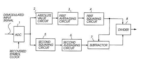
Referring to Figure 1, there is shown a C/N ratio
detector according to a first embodiment of the present invention.
The C/N detector comprises an analog-to-digital converter 1 which
is connected to receive a demodulated 2-PSK signal from a
demodulator, not shown, and driven at a clock rate used to
recover symbols by the demodulator for sampling the demodulated
signal at the recovered symbol rate. An absolute value circuit 2
is connected to the output of the A/D converter to convert the
negative value of the digital output to a positive value and
supplies an absolute value signal to a first averaging circuit 3
the output of which is connected to a first squaring circuit 4
to produce an output representing the carrier component value C.
The output of A/D converter 1 is further applied to a second
squaring circuit 5 to which a second averaging circuit 6 is
connected to produce an output representing the total component
value (C + N). A subtractor 7 is connected to the outputs of the
13 3 3922 71024-92D
circuits 4 and 6 to subtract the output of squaring circuit 4
from the output of averaging circuit 6 to obtain the noise
component value N. A division circuit 8 is connected to the
output of squaring circuit 4 and to the output of the subtractor
7 to determine the ratio C/N.
More specifically, the output of the demodulator is an
analog signal having eye patterns at the recovery timing of
symbols which corresponds to signal points. A/D converter 1
converts the sampled value into n-bit digital data stream di
(where i = 0, 1, 2, ...., n). If n is three, data bit stream
di can be represented as shown in Table 1. This data bit stream
is applied to the absolute value circuit 2 as well as to the
second squaring circuit 5.
Absolute value circuit 2 converts the data di into an
absolute value ¦di¦. As shown in Figure 2, the absolute value
circuit 2 comprises an n-bit polarity inverter 12 and an (n+l)-bit
adder 13. If n=3, polarity inverter 12 comprises exclusive OR
gates 12-1, 12-2 and 12-3 each having a first input terminal
connected to the most significant bit (MSB) position output of
A/D converter 1 and a second input terminal connected to a
respective bit position output of A/D converter 1. The polarity
inverter 12 inverts the logic state of the input of each
exclusive OR gate when the MSB is at logic 1 and applies the
inverted bits to adder 13, while it passes the inputs of all the
exclusive OR gates to adder 13 without altering their logic states
when the MSB is at logic 0. Adder 13 adds MSB of the 3-bit
inputs from A/D converter 1 to the least significant bit (LSB)
of the 3-bit inputs from the polarity inverter 12 and produces
71024-92D
1333~22
4-bit outputs. As a result, absolute values shown in Table 2
are derived.
TABLE 1
Outputs o_ A/D Conv. 1
O
nJ
TABLE 2
Outputs of A.V. Circuit 2
00:
00
00:
0~
O
O
0~ :.
01
Averaging circuit 3 averages the absolute values for a
period of N symbols which is sufficiently long to suppress short
term variations and applies an average value to squaring circuit
4. As shown in Figure 3, averaging circuit 3 comprises an adder
14 connected to the output of averaging circuit 2, a one-sample
delay 15 which is reset at N-symbol intervals and connected
between the output of the adder 14 and a second input of the
adder 15. Adder 14 and delay 15 form an integrator for integrat-
ing N symbols which is divided by a division circuit 16 by a
constant N. Since the noise component contained in digital data
has a Gaussian distribution centered on an amplitude A at zero
noise level, the noise component is cancelled out by the averaging
1 3 3 3 9 2 2 71024-92D
process just described, and therefore, the output of averaging
circuit 3 gives the amplitude of a signal point of the demodulated
signal under noiseless conditions and is represented by Equation
(1) .
N-1
Nl_o I i I (1)
Therefore, the output of squaring circuit 4 supplies a
noiseless carrier component C, or the signal power S, which can
be represented by:
S = A (2)
Since the noise component has a Gaussian distribution
with respect to the amplitude A at a noiseless signal point, the
noise component power ~2 is given by:
2 1 ~ ( ¦ d ¦ -A) 2 (3)
i=O
By substituting Equation (1) into Equation (3), the following
relation is obtained:
N-1d 2 2
N L _o i A ( 4 )
On the other hand, the output of A/D converter 1 is
squared by second squaring circuit 5 and averaged over N symbols
by the second averaging circuit 6 in a manner similar to the
20 processes performed by averaging circuit 3 and squaring circuit 4
just described. As a result, the first term of Equation (4) can
be obtained at the output of averaging circuit 6, namely,
~ + A . Subtractor 7 subtracts the signal power A at the
output of squaring circuit 4 from the (~ + A ) output of
1 3 3 3 9 ~ 2 71024-92D
averaging circuit 6 to derive a noise power a which is used by
division circuit 8 to divide the output A2 of squaring circuit 4.
As shown in Figure 4, division circuit 8 comprises a conversion
table, or a read only memory 17. A set of values S/a2 are
stored in cell locations addressable as a function of variables
S and a2.
Although satisfactory for most applications, the first
embodiment is not suited for systems severely affected by noise.
As shown in Figure 5, the probability density distribution of a
received 2-PSK signal adopts a curve 40 which is a Gaussian
distribution under low noise conditions. Thus, the polarity
inversion of the negative values by absolute value circuit 2
causes the signal point with amplitude -A to be folded over to
the signal point with amplitude A, while maintaining the symmetry
of the curve 40. However, under high noise conditions, there is
an increase in variance a2 of the Gaussian distribution and the
probability density distribution of the received signal adopts
a curve as shown at 41. Therefore, the fold-over effect of the
absolute value circuit 2 will result in a distribution curve 42
under high noise conditions with the result that the average
value of the amplitudes of received signal is shifted to a signal
point with an amplitude A'. The amount of this error increases
with increase in noise. As shown in Figure 6, Eb/No ratios
measured with the circuit of Figure 1 show increasing discrepancy
from theoretical values as the input Eb/No ratio decreases.
A second embodiment of the present invention is shown
in Figure 7. This embodiment eliminates the disadvantage of the
--10 --
1 3 3 3 ~ ~ 2 71024-92D
first embodiment by taking advantage of the forward error coding
and decoding techniques employed in digital transmission systems.
Instead of using the absolute value circuit 2 of Figure 1, the
second embodiment includes a delay 20 connected to the output of
A/D converter 1, an FEC (forward error correcting) decoder 21
for decoding the output of A/D converter 1 and correcting errors
and feeding an FEC encoder 22. The output of encoder 22 is
connected to one input of a polarity inverter 23 to which the
output of delay 20 is also applied. Polarity inverter 23 supplies
a decision threshold to the first averaging circuit 3.
FEC decoder 21 performs error decoding operation on the
output of A/D converter 1 by correcting errors according to a
known error correcting to application to the FEC encoder of a
transmitter, not shown. This signal is applied to FEC encoder 22
in the same way as the transmitter's FEC encoder. With the error
decoding and encoding processes, the output of FEC encoder 22
can be considered more akin to the output of the transmitter's
FEC encoder than the output of the receiver's demodulator is to
it. Therefore, a binary 1 at the output of encoder 22 indicates
that the received input signal is at a signal point having an
amplitude A in a probability density distribution of amplitudes
(Figure 5) and a binary 0 at the encoder output indicates that
the input signal is at a signal point with an amplitude -A.
The output of A/D converter 1 is delayed by circuit 20
by an amount equal to the total delay introduced by decoder 21
and encoder 22 so that the inputs to the polarity inverter 23
are rendered time-coincident with each other.
33~922
- 71024-92D
Polarity inverter 23 uses the output of FEC encoder 22
as a criterion to determine whether the output of the delay 20
lies at a signal point having an amplitude A or at a signal
point having an amplitude -A. In response to a binary 1 from
encoder 22, polarity inverter 23 applies the output from delay
20 without altering its polarity to averaging circuit 3 and in
response to a binary 0, it applies the output of delay 20 to
averaging circuit 3 by inverting its polarity. As shown in
Figure 8, polarity inverter 23 comprises a NOT circuit 30
connected to the output of FEC encoder 22, exclusive OR gates
31-1 to 31-n, and an adder 32. Each exclusive OR gate 31 has a
first input terminal connected to the output of the NOT circuit
30 and a second input terminal connected to a respective one of
the n outputs of the delay circuit 20. Since the output of
delay 20 is represented by 2's complements of the n-bit data,
binary 0 at the output of encoder 22 causes the logic states of
the outputs of delay 20 to be inverted by exclusive OR gates
31-1 through 31-n and summed with a binary 1 from inverter 30
which is summed by adder 32 with the LSB of the n-bit outputs
from exclusive OR gates 31, while a binary 1 at the output of
encoder 22 causes the delay 20 outputs to pass through gates 31
to adder 32 without undergoing polarity inversion.
As a result of this polarity inversion process, the
probability density distribution of the demodulated signal is
centered on the signal point having amplitude A and adopts the
curve 40 of Figure 5 and the average value of the amplitudes of
the received signal rendered equal to the amplitude at the signal
point with amplitude A.
1~ 3 3 ~ 2 2 71024-92D
In this embodiment, the output of the first squaring
circuit 4 can be expressed by the following equation:
~lN-l \2
S = ~N ~oSGN ( i)
where, SGN (di) represents the criterion data from FEC encoder
22.
Figure 9 is a graphic representation of the relationship
between the Eb/No values obtained by circuit of Figure 7 and
theoretical Eb/No values. As is apparent, there is a complete
agreement between the measured and theoretical values down to low
Eb/No input values. This indicates that C/N ratio can be
precisely determined even if the transmission system suffers
severe noise.
To allow accurate determination of C/N ratio, the use
of a powerful error correcting algorithm such as soft decision
Viterbi decoding algorithm or convolutional decoding techniques
is preferred.
Measurement of C/N ratio of a system without interrupt-
ing its service can also be effected alternatively by a third
embodiment shown in Figure 10. This embodiment differs from the
first embodiment by the inclusion of an adaptive weighting
circuit 50.
Since the probability density distribution of the
amplitudes of the received signal adopts a curve A (see Figure
12a) at low noise levels and a curve B at high noise levels
(Figure 12b), at low noise levels the averaged absolute values
of amplitudes becomes approximately equal to the amplitude at
13 3 3 ~ 2 2 71024-92D
the signal point S. However, at high noise levels, the averaged
absolute values result in an asymmetrical curve C with respect
to point S.
The absolute value of the output of A/D converter 1
is taken by absolute value circuit 2 and weighted with a
prescribed weighting factor by the adaptive weighting circuit 50.
Let S(t) represent the signal component of a received signal and
N(t) the noise component. Since noise component has a Gaussian
distribution, an average value N(t) of noise components N(t)
can be regarded as being equal to zero, namely N(t) = 0. The
output signal of the adaptive weighting circuit 50 is applied to
the first averaging circuit 3 where short term variations, i.e.,
noise component N(t) are removed to produce an output ¦S(t)¦W(u),
where W(u) represents the weighting factor, and u = ¦S(t) + N(t)¦.
Therefore, the output signal of the first squaring circuit 4 is
given by S(t) W(u) . This signal is applied to the subtractor 7
and division circuit 8.
By the squaring and averaging operations by the
squaring circuit 5 and the average circuit 6 on the output
{S(t) + N(t)} of A/D converter 1, the input signal applied from
averaging circuit 6 to the subtractor 7 is given by the following
relation:
{S(t)+N(t)}2 S(t)2+N(t)2+2S(t)N(t)
S(t)2+N(t)2+2S(t)N(t) (6)
Since N(t)=0, the third term of Equation (6) becomes zero and so
Equation (6) can be rewritten as:
- 14 - 1333~22
71024-92D
{S(t)+N(t)} =S(t) +N(t) (7)
This weighting factor is determined so that the adverse
fold-over effect produced by taking the absolute values is
minimized. The following conditions are examples of weighting
factor in which the value x represents the output of the absolute
value circuit 2 and TH is a threshold value.
(1) W(x)=x
(2) W(x)=l x >TH
=0 x <TH
(3) W(x)=l x >TH
=-a x <TH
(4) W(x)=x
Figure 11 is one example of the adaptive weighting
circuit 50 which is constructed according to the condition (3).
Weighting circuit 50 comprises a comparator 51, a multiplier 52
and a selector 53 to which the outputs of absolute circuit 2
and multiplier 52 are applied to be selectively coupled to the
division circuit 8. Comparator 51 compares between the output
of the absolute value circuit 2 and a threshold value TH and
applies a logic selection signal to the selector 53. If the
output of absolute value circuit 2 is higher than threshold
value TH, the selection signal is at logic 1 and if otherwise,
the selection signal is at logic 0. Multiplier 52 multiplies
the weighting factor -a on the output of the absolute value
circuit 2 and applies it to selector 53. If the comparator 51
output is at logic 1, the output of absolute value circuit 2 is
passed through the selector 52 to the averaging circuit 3 and if
- 15 ~ 1 3 3 3 ~ 2 2
71024-92D
otherwise, the output of multiplier 52 is passed to the averaging
circuit 3.
Due to the weighting operation, the probability density
distribution of the amplitudes of input signal adopts a curve
shown at D in Figure 12b which is shifted to the right from the
position of curve C (Figure 12a) by an amount equal to the
distance between the intermediate point 0 and the threshold
value TH. The weighting factor -a is so determined that the
noise component which would otherwise cause the most serious
fold-over effect is reduced to a minimum.
Subtractor 7 performs the following subtraction
S(t)2+NIt)2-S(t) W(u)
to produce an output which represents N(t)2, which is applied
to the division circuit 8. As in the first embodiment, the
division circuit 8 comprises a conversion table to which the
signals N(t)2 and S(t)2+N(t)2 are applied as address signals.
Figure 13 is a graphic representation of the characteristic of
the third embodiment using a threshold value 0.25, and a weight-
ing factor -0.5. Comparison between Figures 6 and 13 indicates
that precision of the circuit is improved by as much as 4 dB at
high noise levels (low Eb/No inputs).
The C/N ratio of a demodulator output is found to vary
with a deviation of the frequency of the carrier recovered by
the demodulator from the frequency of the received carrier. The
carrier-to-noise ratio detector of the present invention can
therefore be used instead of the costly automatic frequency
control circuit for preventing the demodulator from being locked
~ 16 ~ 1333922
71024-92D
in a pseudo sync state. This is accomplished by controlling a
voltage controlled oscillator provided in a closed loop of the
demodulator in accordance with the derived C/N ratio such that
the latter is maintained at a maximum level.
As shown in Figure 14, a pseudo sync detector circuit
can be implemented by the C/N ratio detector of the present
invention. A demodulator 60 includes a quadrature detector 61
which receives an input PSK signal at terminal 64 and a recovered
carrier from a voltage controlled oscillator 62 and produces
demodulated signals at terminals 65. The demodulated output
signals are applied to a phase detection and filtering circuit
63 to control the VCO 62 in accordance with a phase difference
detected between the two output signals. One of the output
signals is applied to the input of the C/N ratio detector of
the present invention which is identical to that shown in
Figure 1. The output of the division circuit 8 of the C/N ratio
detector is applied to a controller 66 including a differential
amplifier for comparison with a reference threshold. This
reference threshold corresponds to a DC voltage at which the
VCO 62 generates a carrier at the desired frequency when the C/N
ratio of the demodulator 60 is at a maximum value. The output
of the differential amplifier 66 is representative of the
deviation of the C/N ratio from its maximum value and is applied
to the control terminal of the VCO 62.
When the demodulator is in a sync state, the C/N ratio
of the demodulator is at the maximum value. However, if it goes
out of sync and enters a pseudo sync state, the noise component
- 17 - 1333922
71024-92D
increases in the outputs of the demodulator 60 and hence the C/N
ratio of the demodulator decreases, causing the output of the
differential amplifier 66 to vary correspondingly. In this way,
the VCO frequency is controlled until the output of the division
circuit 8 returns to the maximum value of the C/N ratio.
The foregoing description shows only preferred
embodiments of the present invention. Various modifications are
apparent to those skilled in the art without departing from the
scope of the present invention which is only limited by the
appended claims. Therefore, the embodiments shown and described
are only illustrative, not restrictive.