Note: Descriptions are shown in the official language in which they were submitted.
1 334299
-- 1 --
ELECTRIC LIGHTING AND POWER CONTROLLERS THEREFOR
This inventlon relates to electrical power controllers
which are for use in an AC circuit to control a
lighting load and which particularly, but not
exclusiyely, employ a controllable switch which is
operated so as to conduct during parts of half cycles
of the AC supply. The invention is more particularly,
but not exclusively, concerned with lighting
circuits including luminaires for stage, or
television or film studio, lighting.
A tungsten filament electric lamp functions
essentially as a black body radiator, and accordingly
the spectral characteristics of the lamp are dependent
upon the temperature of the filament and thus upon the
applied RMS voltage. Lamps for luminaires are
typically designed to have a colour temperature of
` 3200K when operating at their rated voltage. A problem
arises, especially in large studios or auditoria that
the large amount of lighting control gear needs to be
sited a substantial distance from the luminaires,
thus requiring lengthy runs of cable to the
luminaires. Even when properly rated cable is used lt
is not unusual for there to be, in a 240V system, a
voltage drop of 5 or even 10 volts along the cable,
1 3342qq
-- 2 --
resulting in a voltage at the luminaire of 235 or even
~30 volts, a reduction in light intensity to 93% or
even 88~, of the rated intensity, and an undesirably
low colour temperature of 3177K or even 3150K.
In a co~our television studio, great care is taken by
the camera operator to set up the camera to achieve a
good colour balance between the colour component
signals of the camera especially to ensure
satisfactory reproduction of skin tones. The colour
balance is affected by the colour temperature of the
lighting, and thus the different colour temperatures
which arise due to voltage drops in the cables present
difficulties to the camera operator in maintaining a
lS good colour balance.
In an attempt to overcome this problem, it has been
known for cables to be used for the luminaires having
- a higher rating than is conventional. High rating
cable is expensive and takes up more room.
A first aspect of the invention is concerned with
solving the above problems. In accordance with this
aspect of the invention, a voltage higher than the
rated voltage of the lamp is applied to the cable
_ 3 1~4~
leading to the lamp and the voltage is adjusted to compensate for
voltage drops in the circuit.
Preferably the compensation is carried out in dependence upon a
value representing the resistance of the cable and the current to
the lamp. Compensation may also be carried out in dependence
upon other voltage drops in the circuit, such as the static and
current-dependent voltage drops which would arise across a
thyristor or triac and a choke in the circuit.
In one embodiment, the current dependency of the compensation
relies directly upon the measured current. In another embodiment,
the current dependency relies upon a predicted value of the load
and a predicted voltage across the load to obtain a predicted
current to the load and the predicted value of the load is
progressively corrected in dependence upon the predicted current
and the measured current.
The invention in one broad aspect provides a method of controlling
power supplied from an AC supply to a lighting load by a circuit
including a controllable switch, the method comprising the steps of
measuring the supply voltage a multiplicity of times over a
half-wave cycle of the supply, producing from the measured voltages
a table indicating how the switch should be operated to obtain any
of a multiplicity of RMS output voltages, receiving a signal
indicative of a desired RMS output voltage, determining from the
table the switch operation required for the desired RMS output
voltage and operating the controllable switch in the determined
manner.
Another aspect of the invention provides a controller for an
electric lighting load, comprising a controllable switch for
connecting an AC power supply to a lighting load and means for
controlling the switch to conduct during a halfwave cycle of the AC
supply for a conduction period less than or equal to the half-cycle
supply period to produce a desired switched output RMS voltage.
The controlling means comprises means to measure the~AC supply
voltage at a multiplicity of sampling times over a half-cycle
period, means to calculate from the measured voltages
- 3A - 1 334299
for each of a plurality of sampling times the RMS voltage which
would be obtained by causing the switch to operate in accordance
with that sampling time, means to receive a signal indicative of
the desired switched output RMS voltage, means to determine the
sampling time for which the calculated RMS voltage corresponds to
the desired RMS voltage and means for operating the switch in
accordance with the determined time in a half-cycle period.
Still further the invention provides a lighting circuit, for
connection to a power supply, comprising a lighting load, a power
controller and means for connecting the lighting load to the power
supply via the power controller, the power controller being
operable to determine the current flowing to the load and to supply
an RMS voltage which is greater than a desired RMS voltage across
the lighting load by an amount dependent upon the determined
current to compensate for the voltage drop along the connecting
means. The power controller is operable to vary the output voltage
in dependence upon a predicted current to the load determined from
the desired voltage across the load and an estimated size of the
load and is operable to measure the output current to the load and
to update the estimated size of the load in dependence upon the
measured and predicted currents.
Further still the invention provides a method of controlling power
supplied from an AC supply to a ~ighting load by a circuit
including a controllable switch, the method comprising the step of
controlling the switch to conduct during each or every alternate
half-wave cycle of the AC supply for a conduction period less than
the half-cycle period to produce a desired RMS output voltage,
characterized by the steps of determining the current to flow to
the load, compensating in the switch controlling step for a voltage
drop in the circuit due to the resistance of the circuit in
accordance with the determined current and further compensating in
the switch controlling step for a voltage drop across the
controllable switch at substantially zero current.
There follows a description by way of example of a specific
embodiment of the invention and modifications thereto, with
~ reference to the accompanying drawings in which:
1 334299
-- 4 --
Figure 1 is a block diagram of a lighting system;
Figure 2 is an equivalent power circuit for each
dimmer channel;
Figure 3 is a block diagram of one of the dimmer
processors of Figure 1;
Figures 4A and 4B are flow charts of the processes
carried out by the dimmer processor of Figure 3;
Figure 5 is a block diagram of one of the dimmer units
of figure 1;
Figure 6 is a block diagram of a modified dimmer
processor;
Figure 7 is a flow chart of the processes carried out
by the dimmer processor of Figure ~;
Figure 8 is a voltage-time graph of a mains
half-cycle;
Figure 9 is a block diagram of the mains compensation
processor of Figure 1: and
- s ~ 334~qq
Figure 10 is a flow chart of the process carried out
by the main~ compensation processor of Figure 9.
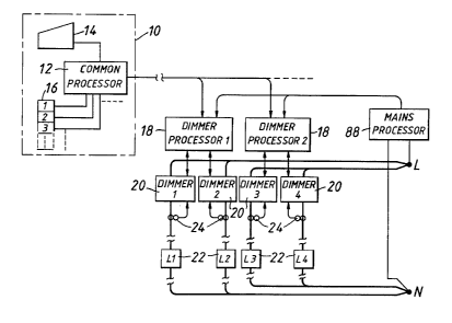
Referring to Figure 1, a lighting control system is
shown which includes a lighting control desk 10 havlng
a common processor unit 12, a data input terminal 14
and a bank of faders 16 for respective dimmers. The
common processor unit 12 sends data to one or more
dimmer processors 18, two of which are shown for
simplicity. Each dimmer processor controls one or more
dimmers 20, two of which are shown for each dimmer
processor 18. Each dimmer 20 is connected in series
with a load 22 across a mains supply L-N and is
associated with a respective current sensor 24.
Referring to Figure 2, an equivalent power circuit is
shown for each dimmer channel. An RMS voltage Vi is
~ supplied by the mains L-N to a controllable switch,
such as a thyristor 26, which is closed part-way
through each mains half-cycle and opens at the end of
the cycle, producing a switched output RMS voltage Vs.
A current-independent RMS voltage drop Vd arises
across the thyristor 26. The thyrlstor 26 and
associated dimmer components such as a filtering
inductor also act as resistor, represented by Rd,
across which there is an RMS voltage drop IoRd, where
- 6 - l 3 3 42 9 q
Io is the RMS output current. The connecting cable of
the circuit also acts as a resistor, represented by
Rc, across which there is an RMS voltage drop IoRc.
It will therefore be appreciated that the RMS voltage
Vl across the load 22 will be:
Vl = Vs - Vd - Io (Rd + Rc)
and that Vs will be a function of the supply voltage
and the conduction period in each half cycle of the
switch 26.
Referring to Figure 3, there is shown a block diagram
of one of the dimmer processors 18. The processor
includes an input/output port 28, which receives
digital signals Cl, C2, representing the settings of
the desired levels for the respective dimmer channels
1 and 2. The signals C for all of the dimmer channels
may be transmitted from the processor of the control
desk as time-division-multiplexed signals, or as
signals associated with addresses of the respective
channels, all on a single line. Alternatively, the
control signals C may be transmitted as digital or
analogue signals on separate lines. The input port
also receives output current signals Iol, Io2 from
1 33429q
the respective dimmers 20,and supplies timing signals
Tl, T2 to the respective dimmers.
The dimmer processor 18 also includes a microprocessor
30, a program ROM 32, and a RAM which stores various
tables and variable values. For each dimmer channel
there is a look-up table 34 which relates RMS load
voltage Vl to control value C (only one table 34 is
shown for simplicity). In common for all dimmer
channels controlled by the respective dimmer
processor, there are (a) a look-up table 36 which
relates predicted RMS current Ip' to the RMS load
voltage Vl for a tungsten filament load of
predetermined rating, for example lkW;- and (b) a
look-up table 38 which relates thyristor conduction
angle A to the switched output RMS voltage Vs. In
common for all of the dimmer channels, the RAM stores
a value f of the mains frequency, and for each dimmer
channel it stores the resistance values Rd, Rc and
thyristor static voltage drop value Vd, mentioned
above, and also a value W of the power of the
respective load 22.
For each dimmer channel, the dimmer processor 18
performs two processes as shown in Figures 4A and 4B.
Figure 4A shows a feed-forward loop for receiving the
?~
,J
- 8 - 1 3 3 4 299
control signal C and outputting the timing value T. In
step 40, the value of C ls taken from the I/O port 28.
In step 42, the table 34 is used to look-up the RMS
load voltage Vl to be supplied for the value C. In
S step 44, the table 36 is used to look-up an RMS
current Ip' which it is predicted would flow if the
load were a lkW tungsten filament lamp. In step 46,
the value Ip' is scaled by the factor W which is the
curently stored value of the power of the load (in kW)
to obtain the predicted current Ip to the load. In
step 48, the required switched output RMS voltage Vs
is calculated using the equation mentioned above with
reference to Figure 2 and the stored values of Rd, Rc
and Vd. In step 50, the table 38 is used to look-up
the firing angle A which is required to provide the
calculated switched voltage Vs. In step 52, the
firing timing T after the start of a half-wave cycle
is calculated from the equation T = A/(2.pi.f) using
the stored value of f. In step 54, the calculated
value T is sent via the I/O port 28 to the respective
dimmer 22. The process is then repeated.
Figure 4B shows a feed-back process performed by the
dimmer processor 18. In step 56, the value Io of the
measured output current is taken from the I/O port 28.
It is then determined in step 58 whether the measured
-
9 1 3342~9
current Io is equal to the predicted current Ip
utilised in the process of Figure 4A. If so, the
process of figure 4B loops back to ths beginning.
However, if there is an lnequality, $n step 60 the
S stored load value W is incremented by an amount
proportional to the difference between measured load
current Io and the predicted load current Ip. The
process then loops back to the beginning.
Reference is now made to Figure S which illustrates
one of the dimmers 20. A pair of thyristors 62', 62"
are connected oppositely in parallel in the power line
from the mains supply to the load. An inductor 64 is
included for filtering, and a current sensor 66, for
example in the form of a multi-turn coil of wire, is
placed on the load side of the thyristors and provides
a analogue signal proportional to the load current.
The dimmer also includes a circuit 68 including an
analogue-to-digital converter 70 to convert the
detected current signal to a digital value Io and a
register 72 for storing the detected current value.
An input/output port 74 is included for outputting the
detected current value Io to the dimmer processor 18,
and for receiving from the dimmer processor 18 the
2S firing time value T in the form of 10 bit data, which
is passed to a timing register 76. The circuit 68
` -
- 10 - 1 3 3 42 9 q
also includes a ten bit timebase 78 controlled by a
crystal 80. The timebase 78 is reset by a
zero-crossing signal provided by a zero-crossing
detector 82 connected to the supply line. Resetting
occurs at the beginning of each half-cycle of the
mains. The outputs of the timebase 78 and the timing
register 76 are compared by a comparator 84, and once
the timebase output has increased so as to equal the
content of the timing register 76, a signal is
provided to a driver circuit 86 which supplies
appropriate pulses to the gates of the thyristors 62',
62N so that the appropriate thyristor conducts for
the remainder of the half-cycle.
It will be appreciated from the above that for each
dimmer channel the respective dimmer processor
provides a conversion from the control value C to the
firing timing T taking into account the desired dimmer
transfer characteristic (Table 34) and the voltage
drop in the circuit. The voltage drop is calculated
on the basis of a predicted current in order to avoid
high errors in compensation due to transmission delays
and to processing delays in the event of the control
value C being rapidly changed. For example, if the
control value C is suddenly increased from a minimum
value to a maximum value, a current higher than the
1 33~299
11
steady state current will initially flow through the
lighting load, until the steady state temperature and
resistance of the lamp filament are reached. If the
voltage drops were determined from the measured
S current, rather than the "predicted" current, then
until the high transient current value has been
measured, transmitted and processed, under-
compensation would be provided for the voltage drop in
the circuit. Once the high transient current had been
measured and processed, over-compensation would be
provided, because by that time the transient would
have passed and the steady state reached. By utilising
a "predicted" current determined from the filament
characteristic (Table 36) and the stored load, the
errors in compensation during transients are reduced,
and by adjusting the stored load value (Figure 4B),
steady state compensation is correctly achieved.
It is possible that, in some applications, the errors
in compensation described above could be minimised and
tolerated. In this case, a simplifled system can be
used, in which the dimmer processor is modified as
shown ln Figure 6 and performs a slngle process as
shown ln Flgure 7, rather than the two processes shown
in Figures 4A and 4B. The dimmer processor of Figure
6 ls similar to that of Figure 3, with the exception
1 33429~
- 12 -
that there is no Table 36 relating RMS load voltage Vl
to predicted current Ip', and there is no storage of a
variable W. The process of Figure 7 ls simllar to
that of Figure 4A, with the exceptlon that steps 44
and 46 are replaced by the single step 45 of taklng
the measured load current Io from the I/0 port 28, and
step 48 is modified as shown in step 48' to compute
the voltage drop across the dimmer and cable
resistances Rd, Rc directly from the measured load
current Io, so that the desired switched output RMS
voltage Vs is determined from the equation:
Vs = Vl + Vd + Io(Rd + Rc)
It will be appreciated that, in order to permit the
system to compensate for voltage drops and be able to
supply -the rated voltage, say 240V, to the loads, the
input supply voltage must be greater than the rated
voltage. This is achieved by supplying power through
an auto-transformer which steps up the supply
voltage from, for example, nominally 240V to 264V, or
by using a special high voltage mains supply of, for
example, 264V.
1 33429~
- 13 -
The controlling operations of the dimmer system have
been described above, but it will be appreciated that
the system must firstly be initialised to set up the
common Tables 36, 38, the common variable f, the table
34 for each dimmer, and the variables Rc, Rd, Vd for
each di-mmer, and the initial load value W for each
dimmer. The tables 34 to 38 may be stored in
non-volatile memory associated with each dimmer
processor 18. Alternatively, they may be stored in
non-volatile memory associated with the common
processor 12 and be down-loaded to the dimmer
processors in an initialisation process. In this
case, the dimmer transfer function Table 34 to be used
for each dimmer may be selected, using the terminal
14, from any of a set of different tables providing,
for example, a square-law transfer function, a linear
function, a constant function, or a specially
programmed function. The mains frequency value f may
be measured by the dimmer processor 18 or by a mains
processor 88 (Figure 1) connected across the mains
supply L-N and supplying the frequency value f to the
I/0 ports 28 of the dimmer processors either merely
during the initialisation process, or repetitively
during the operation of the system. The values Rc,
Rd, Vd and W for each channel may be entered by the
terminal once the system is commissioned and stored in
1 33429~
- 14 -
non-volatile memory associated with the common
processor 12, and then be down-loaded to the dlmmer
processors 18 each time the system is initialised.
Alternatively, these values may be sent to the dimmer
processors when the system is commissioned and stored
in nonevolatile memory associated with the dimmer
processors.
In the system described above, it has been assumed
that the Table 38 relating desired switched output RMS
voltage Vs to required firing angle A is an invariable
table. In one modification, in order to compensate for
variations in the mains RMS voltage, the voltage Vs
used as the address for Table 38 may be scaled by a
factor of Vr/Vm, where Vr is the rated mains RMS
voltage and Vm is a measured value of the actual mains
RMS vol-tage. Whilst this may be satisfactory for some
applications, it will be appreciated that other
perturbations in the mains supply will cause
variations in the required firing angle A to produce a
desired switched output RMS voltage Vs.
Referring to Figure 8, a nominal mains half wave cycle
is denoted by reference numeral 90 and is of perfect
sine form, having a peak value which is root-two times
the rated RMS voltage. In practice, however, various
' -
1 3342q9
-- 15 --
errors arise in the mains wave form. Firstly, the
voltage may be generally low as shown by curve 92, or
even high. Secondly, the peak of the wave may be
suppressed due to saturation effects in the
transformers of the supply network, as denoted by
curve 9~. Furthermore, in a theatre, or a television
or film studio, where a large number of
dimmer-controlled loads are in use, a progressively
larger load may be imposed on the mains as the mains
half-cycle progresses, thus pulling down the supply
voltage as the half-cycle progresses, as shown by
curve 96. These various perturbations in the mains
supply all effect the switched output RMS voltage Vs
which is, in fact, obtained for a given firing angle
A. The mains processor 88 (Figure 1) is included to
compensate for these perturbations by supplying to the
dimmer processors 18 data for the Tables 38 (Figure 3)
derived from measurement and processing of the mains
wave form, rather than including in the Tables 38
fixed theoretical data for a perfect form and
amplitude of mains supply wave.
Referring to Figure 9, the mains processor 88 includes
an input from the mains L which is applied, through a
low-pass analogue filter 98, which removes any high
frequency interference on the signal, to an analogue
- 16 - 1 3 3 4 2 qq
to digital converter 100, which applies a digital
voltage signal V to an input/output port 102 for a
processor 104. The processor 104 has associated ROM
106 and RAM including storage for three tables 108,
110, 112 and for a variable f.
The process carried out by the processor 104 is
illustrated in Figure 10. In steps 114 to 118, a
variable t is reset and the voltage value V is
repeatedly tested in a loop until a zero-crossing is
detected in which the value V is substantially equal
to zero. Then, the value of V is stored at an address
corresponding to the time variable t in Table 108, in
step 120. After a predetermined delay in step 122,
the time variable for t is incremented in step 124.
Then, in step 126, a fresh value for the voltage
variable V is detected, and in step 128 it is tested
whether the value V is substantially equal to zero
indicating the end of a half-cycle period. If it is
not, then the process loops back to step 120, where
the value of the variable V is stored in Table 108 at
an address t corresponding to the incremented time
variable. It will therefore be appreciated that whlle
the loop of steps 120 to 128 is running the Table 108
is built up of the instantaneous voltage of the mains
over one half-cycle period. At the end of the
` -
- 17 - 1334299
half-cycle period, in step 130, the mains frequency f
is computed from the equation f = 1/(2t) and is stored
in the RAM. Then, in steps 132 to 138, a loop process
is performed for each value of firing angle variable
S A from pi to zero, with a step of -pi/1024. In this
loop, ~n step 134, the RMS voltage Vs over the
half-cycle period is computed for the voltage signals
in Table 108 between the time A/(2.pi.f) and the time
at the end of the half-cycle period, that is 1/(2f).
In step 136, the computed RMS voltage signal Vs is
stored in the Table 110 at an address corresponding to
the firing angle A. It will therefore be appreciated
that once the Table 110 has been completed, it stores
the switched output RMS voltage which will be obtained
for any of 1024 firing angles A over the half-cycle
period. In step 140, the processor 104 performs an
operation to invert the Table 110 and store it as
Table 122, in which required firing angle A can be
looked up for any required switched output RMS voltage
Vs. In step 142, the variable f is sent to the I/0
port 102 for transmission to the dimmer processors 18,
and in step 144, the look-up table 112 is sent to the
I/0 port 102 for transmission to the dimmer processors
and storage as Table 38 in each of the dimmer
processors (see Figure 3). Thus, each of the dimmer
processors 18 has stored a look-up table of firing
- 18 - l 3~4~9 q
angle A against switched output RMS voltage Vs which
has been derived by measuring the mains wave form,
rather than a theoretical look-up table.
Since the transmission of the Table 112 will entail
heavy data traffic, either one of two modifications
may be made to the process shown in Figure lO. In one
modification, after step 142, a low-pass digital
filter process is applied to the data in Table 112
prior to transmission in order to reduce the amount of
data. Then, when the Tables 38 are set up in the
dimmer processors 18, an interpolation operation can
be carried out to obtain values of firing angle A for
voltages Vs intermediate the values which have been
transmitted.
In the-second modiflcation, in step 148, a delta
process is applied to the data in Table 112, so that
rather than transmitting the absolute firing angle
value A for each voltage Vs, the difference between
that firing angle value A and the previous flring
angle value A ls transmitted. Therefore, less bits of
data will be required to be sent.
1 33429q
-- 19 --
Referring to Flgure 1, a single malns processor 88 has
been shown for all of the dimmer processors. In a
modification to this arrangement, in order to avoid
the heavy amount of data trafflc from the mains
processor 88, the mains processing may be carried out
by each-dimmer processor 18 so that the Table 112
produced in the mains processing also serves as the
Table 38 for the dimmer processing.
It will be appreciated that in the case where a
theatre or studio is supplied with a three-phase mains
supply, then there will be differences between the
mains wave form on each of the three phases. In order
to account for this difference, three mains processes
may be carried out, one for each phase, and the dimmer
processors may refer to the appropriate look-up table
in dependence upon which phase is being used to power
the lighting load in question.
Whilst the embodlment of the inventlon described above
utilises power control by thyristors which are gated
on and remain on for the remainder of the half-cycle,
it will be appreciated that the lnventlon is also
applicable in the case where gate turn-off thyristors
are used, or in the case where pulse-width-modulated
switching devices are employed. The invention may
- 20 - 1 334299
also be put into practice using a variable resistor or
transformer for varying the power supplied to the
load.