Note: Descriptions are shown in the official language in which they were submitted.
1 334304
The present invention relates to a packet switch
for high-speed packet communications.
In parallel with the rapid progress in the
optical fiber transmission and high-speed VLSI (Very Large
Scale Integrated Circuit) technologies, there is an
increasing demand for new communication services of the
kind using extremely fine pictures, for example. While
broadband ISDN's (Integrated Services Digital Networks) are
available as means for handling a plurality of different
kinds of information such as voice and pictures
collectively, how to multiplex and switch such various
kinds of information is a critical consideration. An STM
(Synchronous Transfer Mode) switching scheme and an ATM
(Asynchronous Transfer Mode) switching scheme have been
proposed to implement the multiplexing and switching
systems of broadband ISDN's.
With an ATM switching scheme, motion picture,
voice or similar continuous data and a still picture or
similar burst data are packetized into fixed length packets
and the packets are exchanged. The ATM switching scheme
does not require that the terminal equipment and
transmission channels be synchronous and be provided with
the same data rate. This kind of switching scheme is
therefore advantageous over an STM switching scheme with
regard to the ease of system expansion and development. An
example of packet switches applicable to an ATM switching
scheme has been taught by Thomas et al in a paper entitled
"ASYNCHRONOUS TIME-DIVISION TECHNIQUES: AN EXPERIMENTAL
PACKET NETWORK INTEGRATING VIDEO COMMUNICATION",
International Switching Symposium, (ISS) '84 Florence, May
7-11, 1984, Session 32 C, Paper 2 (Reference 1). As
described later in detail, the packet switch disclosed in
this paper has a single buffer memory which is shared by
multiple input lines and multiple output lines, and it
switches packets by controlling the write and read
addresses of the buffer memory. The address control of the
- 1 - -~
- 1 334304
buffer memory is effected by using address queues which are
assigned to individual output lines, a waiting address
queue which shows addresses of stored packets, an idle
address queue which shows idle areas of the memory, etc.
While this system can be implemented with a relatively
small buffer memory capacity because multiple output lines
share the memory, it requires complicated control for the
shared use of the memory. Specifically, idle address queue
and waiting address queues associated with the individual
output lines are required, and addresses have to be
interchanged between the idle address queue and the waiting
address queues every time a packet is written in or read
out of the buffer memory. Moreover, when a certain address
in a queue is lost or doubled by noise or some malfunction,
there occurs in the buffer memory an unused area or, in the
worst case, false data is overwritten on a packet to delete
the latter or a packet is fed out to an unexpected output
line. Such occurrences cannot be eliminated without
resorting to extra means for detecting unusual conditions
and, because such detection is difficult, the processing is
complicated.
It is therefore an object of the present
invention to provide a packet switch which is easy to
control and highly reliable.
It is another object of the present invention to
provide a packet switch configuration which can be readily
implemented as an integrated circuit.
Accordingly, one aspect of the invention provides
a packet switch, having a plurality of input lines and a
plurality of output lines for exchanging packets received
over said input lines and delivering exchanged packets to
said output lines, comprising:
(a) a plurality of first serial-to-parallel
converting means each being associated with a respective
one of said input lines for converting a packet coming in
over an associated one of said input lines to first
` 1 334304
- parallel data having a first predetermined number of bits,
while latching address information contained in said
packet;
(b) a plurality of unit packet exchanging means
equal in number to said first predetermined number, each
comprising
(i) a plurality of second serial-to-parallel
converting means each being associated with one of said
plurality of first serial-to-parallel converting means for
receiving an associated bit of said first parallel data as
input serial data, for converting said input serial data
into second parallel data having a second predetermined
number of bits,
(ii) a plurality of memory means each being
associated with one of said output lines for storing said
second parallel data, in response to a write signal, as
stored data and for outputting said stored data at a
predetermined period,
(iii) first bus means for distributing said
second parallel data to said plurality of memory means, and
(iv) a plurality of first parallel-to-serial
converting means each being associated with one of said
plurality of memory means for converting said second
parallel data to first serial data and outputting said
first serial data as an associated bit of said first
parallel data; and
(c) address controller means comprising
(i) a plurality of third serial-to-parallel
converting means each being associated with one of said
first serial-to-parallel converting means for converting
said address information to parallel address data,
(ii) a plurality of address filter means each
being associated with one of said plurality of output lines
for making a determination whether or not said parallel
address data indicates said one of said output lines and,
1 334304
- if the result of said determination is positive, outputting
said write signals, and
(iii) second bus means for distributing said
parallel address data to said plurality of address filter
means; and
(d) a plurality of second parallel-to-serial
converting means being associated with respective ones of
said plurality of output lines for reading said first
serial data from said first parallel-to-serial converting
means of said plurality of unit packet exchanging means for
converting said first serial data to second serial data and
delivering said second serial data as said exchanged
packet.
Another aspect of the invention provides a packet
switch having a plurality of input lines and a plurality of
output lines, for exchanging packets received over said
input lines and delivering exchanged packets to said output
lines, comprising a plurality of first serial-to-parallel
converting means each being associated with a respective
one of said input lines for converting a packet coming in
over an associated one of said input lines to first
parallel data having a predetermined number of bits, while
latching address information contained in said packet, a
plurality of unit packet exchange means each being
associated with a respective one of said bits of said first
parallel data, and a plurality of first parallel-to-serial
converting means being associated with a respective one of
said plurality of output lines for reading said first
parallel data out of an associated one of said memory
means, converting said first parallel data to first serial
data as an exchanged packet to an associated one of said
output lines, each of said plurality of unit packet
exchange means comprising a plurality of second serial-to-
parallel converting means each being associated with said
plurality of first serial-to-parallel converting means for
receiving associated bits of said first parallel data as
-- 4 --
1 33430~
~ input serial data, converting said input serial data into
second parallel data having a second predetermined number
of bits, combining said address information being latched
by an associated one of said first serial-to-parallel
converting means with said second parallel data to produce
third parallel data, a plurality of address filter means
each being associated with said plurality of output lines
for determining whether or not said third parallel data is
meant for said associated output line by referencing
address information of said third parallel data and, if a
result of a decision is positive, outputting said second
parallel data by removing said address information from
said third parallel data , bus means for distributing said
third parallel data from one of said second serial-to-
parallel converting means to all of said address filtermeans, memory means each being associated with said address
filter means for holding as write data said second parallel
data which is outputted by an associated one of said
address filter means and outputting said write data at a
predetermined period; and a plurality of second parallel-
to-serial converting means each being associated with said
memory means for converting said second parallel data
outputted by an associated one of said memory means to
second serial data and outputting said second serial data.
Embodiments of the present invention will now be
described, by way of example, with reference to the
accompanying drawings, in which:
Figure 1 is a schematic block diagram showing a
prior art packet switch:
Figure 2 is a schematic block diagram showing a
first embodiment of the present invention;
Figure 3 is a schematic block diagram showing a
second embodiment of the present invention;
Figure 4 is a schematic block diagram showing a
third embodiment of the present invention;
1 334304
Figure 5 is a schematic block diagram showing a
fourth embodiment of the present invention;
Figure 6 is a schematic block diagram showing a
specific LSI configuration of the packet switch shown in
Figure 4;
Figures 7a to 7c are diagrams demonstrating the
operation of the packet switch shown in Figure 6;
Figure 8 is a schematic block diagram showing a
first modification of the construction shown in Figure 6;
Figure 9 is a schematic block diagram showing a
second modification of the Figure 6 construction; and
Figure 10 is a schematic block diagram showing a
third modification of the Figure 6 construction.
In the figures, the same components and
structural elements are designated by like reference
numerals.
To better understand the present invention, a
brief reference will be made to a specific construction of
the previously mentioned packet switch proposed by Thomas
et al., shown in Figure 1. In this figure, various kinds
of data each having a predetermined packet configuration of
a fixed length come in over a plurality of input lines 2001
to 200N. A multiplexer 202 receives all of the packets
coming in over the input lines 2001 to 200N and multiplexes
them on a packet basis. Assuming that the bit rate of each
input line is V (bit/s) and that the number of input lines
is N, the bit rate of the multiplexed packet is VN (bit/s).
The multiplexed packet outputted by the multiplexer 202 is
fed to a buffer memory 203 and an address filter 204. In
response, the address filter 204 extracts output line
information (an output line address) associated with the
arrived packet and applies it to a selector 208, while
delivering a write enable signal WE to the buffer memory
203. A write address queue 205 storing the addresses of
unoccupied or empty areas of the buffer memory 203 feeds to
the buffer memory 203 and the selector 208 a write address.
~n
1 33430~
-
The buffer 203 stores the packet in response to the write
address and the write enable signal WE. Connected to the
selector 208 are read address queues 207 which are
associated with individual output lines 213 and may each be
implemented by a First-in First-out (FiFo) memory. The
selector 208 delivers the write address from the write
address queue 205 to one of the read address queues 207
which is associated with the output line address fed from
the address filter 204.
Implemented as a dual port memory, for example,
the buffer memory 203 is constructed such that packets are
read out independently of packet writing in response to a
read clock which is fed from the output line side. A
counter 209 counts the read clock and cyclically produces
the output line address.
A selector 210 is responsive to the output of the
counter 209 to select any one of the read address queues
207. When any of the address queues 207 selected by the
selector 210 does not store any addresses to be read, it
produces a special address (dummy address). For the dummy
address, use may be made of any numerical value which is
never used for the addresses of the buffer memory 203 by
way of example.
A dummy packet generator 211 receives the read
address of the buffer memory 203 via the selector 210 and
determines whether it is a dummy address or not. If the
read address is a dummy address, the dummy packet generator
211 does not read a packet out of the buffer memory 203
but, instead, delivers a dummy packet which is used for
timing extraction and synchronization of the system, to a
demultiplexer 212. If the read address is not a dummy
address, the dummy packet generator 211 applies the value
of the read address to the buffer memory 203 together with
a read enable signal RE so as to read out a packet. The
address from which the packet has been read and is
therefore empty is written into the write address queue
1 334304
- 205. The demultiplexer 212 demultiplexes the packets from
the buffer memory 203 or the dummy packet generator 211
into the output lines 2131 to 213N. The procedure
described above is repeated to execute packet switching.
This prior art packet switch has a single buffer memory
which is shared by a plurality of output lines and is
therefore successful in reducing the required capacity of
a buffer memory, it renders the address control
complicated, as discussed earlier.
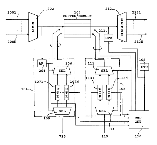
10Referring to Figure 2, a first embodiment of the
packet switch in accordance with the present invention is
shown. In the figure, fixed length packets arrive at input
lines 2001 to 200N on a time division basis. A multiplexer
202 multiplexes those packets on a time division basis and
delivers the multiplexed packets to a buffer memory 103 and
a write address controller 104. The buffer memory 103 is
divided into N memory areas each being associated with a
different output line of N output lines 2131 - 213N. These
memory areas may have the same size and may be provided
with addresses in the same manner, for example. The write
address controller 104 includes an address filter 204 for
extracting from the input packet the destination address
which is associated with the destined output line. More
specifically, the address filter 204 determines to which
output line the input packet should be directed and, for
example, produces an output line number indicating the
particular output line. The output line number is
delivered to the buffer memory 103 and a selector 106.
Connected to the input of the selector 106 are write
address counters or write address pointers 1071 to 107N
associated with the individual output lines 2131 to 213N,
and each generates a write address of the associated memory
area of the buffer memory 103. In response to the output
line number from the address filter 204, the selector 106
selectively feeds to the buffer memory 103 a value of the
associated counter as a write address. Hence, the packet
1 33430~
- is written in a particular address of a particular area as
designated by the write address from the selector 106 and
the output line number from the address filter 204. The
output line number from the address filter 204 is also fed
to a selector 109. In response, the selector 109
selectively feeds an externally derived increment clock 112
to the counters 1071 to 107N to increment the contents of
the counters.
On the other hand, packet reading is performed
independently of the packet writing in response to a read
clock which is fed from the output line side. A counter
108 counts the incoming read clock and sends its output to
a comparing circuit 110. A read address controller 105
comprises two selectors 111 and 114, and read address
counters 1131 to 113N. The comparing circuit 110 compares
the write addresses of the counters 1071 to 107N and the
read addresses of the counters 1131 to 113N in response to
the value of the counter 108. When the value of one of the
read address counters 1131 to 113N and that of the
corresponding one of the write address counters 1071 to
107N are the same, a packet to be read out does not exist
in the memory area associated with the output line as
designated by the counter 108. In this case, the comparing
circuit 110 commands a dummy packet generator 211 to
generate a dummy packet. Meanwhile, when the values of the
read and write counters are not the same, the comparing
circuit 110 delivers the value of the counter 108 to the
buffer memory 103 and selectors 111, 114. The selector 111
selects any one of the counters 1131 to 113N which is
indicated with the value of the counter 108. Hence, a
packet is read out of a particular address of a particular
memory area of the buffer memory 103 as designated
respectively by the value of particular one of the counters
1131 to 113N and the value of the counter 108.
The packets read out of the buffer memory 103 or
the dummy packets are fed to a demultiplexer 212. The
- 1 334304
demultiplexer 212 demultiplexes the packets into an
individual packet, which is supplied to the output line
indicated by the value of the counter 108. The selector
114, in response to the output of the counter 108,
selectively supplies an increment clock pulse to the
counters 1131 to 113N to increment their contents.
In the illustrative embodiment, adjustment is of
course made such that the packet read clock and the
operation clock of the demultiplexer 212 are coincident,
and such that the area for reading out a packet and the
output line to which the demultiplexer 212 distributes the
packet accurately correspond to each other.
Packet switching is accomplished by the packet
writing and packet reading described above.
An advantage attainable with this embodiment is
that since the buffer memory 103 is divided into a
plurality of memory areas each being associated with a
different output line, the addresses of the individual
areas can be controlled by counters without a complicated
address exchange which is required in the prior art.
Referring to Figure 3, a second embodiment of the
present invention is shown which assigns independent buffer
memories to the individual output lines and performs
address control line by line. In this figure, packets
coming in over a plurality of input lines 2001 to 200N are
multiplexed by the multiplexer 202 by the same procedure as
in the first embodiment of Figure 2. The multiplexed
packet is fed to buffer units 2501 to 250N each being
individually assigned to a different output line. Each
buffer unit has an address filter 120, an address
controller 124, a buffer memory 122, and a dummy packet
generator 130. The address filter 120 detects the
destination address from the packet and sends the packet to
the buffer memory 122 when the detected address represents
the address of the unit 2501 itself. The address filter
120 also delivers a write enable signal to the address
-- 10 --
1 334304
controller 124 upon the detection of the destination
address of the unit 2501. The address controller 124 has
a write address counter or pointer 126, a read address
counter or pointer 128 and comparator 127. In response to
the write enable signal from the address filter 120, the
write address counter 126 delivers the write address to the
buffer memory 122 having a FiFo configuration, and then
increments the write address counter 126 by 1.
On the other hand, packets are read out of the
buffer memories 122 on the output line 2131 in response to,
for example, a read clock which is generated by a clock
pulse generator, not shown. The comparator 127 of the
address controller 124 compares the read address of the
counter 128 and the write address of the counter 126 upon
reception of the read clock pulse.
If both read and write addresses are different
from each other, the comparator 127 feeds a read control
signal to the read address counter 128. In response to the
read control signal, the read address counter 128 supplies
the read address to the buffer memory 122 together with a
read enable signal and increments its own value by one. If
the read address from the counter 128 is identical with the
write address from the counter 126, the comparator 127
delivers a dummy packet insertion command to the dummy
packet generator 130. In response, the dummy packet
generator 130 generates a dummy packet having a
predetermined format and, in synchronism with the readout
of a packet from the buffer memory 122, delivers the dummy
packet to the output line 2131. The format of the dummy
packet is dependent upon the protocol of data transmission.
This particular embodiment of Figure 3 eliminates the need
for a demultiplexer because the buffer unit having the
address filter 120, the address controller 124 and the
dummy packet generator 130 are assigned to each of the
output lines 2131 to 213N.
-- 11 --
- 1 334304
Figure 4 shows a third embodiment of the present invention using input buffers 1401 to 140N which are
individually assigned to the respective input lines 2001 to
200N. The input buffers 1401 to 140N and the buffer units
2501 to 250N which are provided on the output lines 2131 to
213N are interconnected by a bidirectional bus 142. The
input buffers 1401 to 140N and bus 142 co-operate as the
multiplexer 202 shown in Figure 3. Each of the input
buffers 1401 to 140N temporarily stores a packet coming in
over its associated input line in response to a write clock
whose frequency is the same as the transmission speed of
the incoming packet. The input buffers 1401 to 140N also
receive a read clock which cyclically supplied from an
external clock pulse generator. In response to the read
clock, the input buffers 1401 to 140N sequentially deliver
the stored packet to the bus 142 on a time division basis
so that a multiplexed packet is on the bus 142.
The packet on the bus 142 is fed to all of the
buffer units 2501 to 250N. This is followed by the same
procedure as in the embodiment of Figure 3.
Figure 5 shows a fourth embodiment of the present
invention in which the bus is formed in a loop
configuration.
In the embodiment shown in Figure 4, a
bidirectional bus is used for the bus 142 since the
direction of the data transmission depends on the position
of input buffers along the bus 142. For example, in Figure
4, the direction of the packet which the input buffer 1401
transmits to the buffer unit 250N is different from the
direction of the packet which the input buffer 140N
transmits to the buffer unit 2501. The loop configuration
allows a unidirectional bus which is economical compared
with a bidirectional bus.
In Figure 5, each of the buffer units 2501 to
250N is assigned to each of the output lines 2131 to 213N
similarly with the embodiment shown in Figures 3 and 4.
- 12 -
C
1 334304
A characteristic feature of this particular
embodiment is that each of bus control circuits 1541 to
154N for sending data to a unidirectional bus 152 is
associated with each of the input lines 2001 to 200N. As
shown, each of the bus control circuits 1541 to 154N
comprises a first memory 150 for temporarily storing a
packet fed over associated one of the input lines 2001 to
200N, a second memory 155 for temporarily storing a packet
from the unidirectional bus 152, and a selector 153 for
routing either one of the packets stored by the first and
second memories 150 and 155 to the unidirectional bus 152
in response to an external selecting signal which is fed
thereto.
The selector 153 selects data from the first
memory 150 and sends it to the unidirectional bus 152 when
it receives the selecting signal indicative of the data
transmission timing of its associated input line, whereas,
it feeds data from the second memory 155 with no selecting
signal. For example, assuming that the number of the input
lines is N and the speed of the operation clock of the
selector 153 is U, the selector 153 receives the selecting
signal in a U/N period, which has a phase difference of l/N
for the selecting signal supplied to the adjacent selector.
By such an operation of the selector 153, packets
coming in over the respective input lines are sequentially
fed out to the unidirectional bus 152. The unidirectional
bus 152 extends across all of the bus control circuits 1541
to 154N, so that packets on the unidirectional bus 152 are
routed to all of the buffer units 2501 to 250N. The
following operation is the same as the operation previously
discussed in relation to the second and third embodiments
shown in Figures 3 and 4.
Now, the integrated circuit implementation for
the previously discussed packet switch will be considered.
Among the four different embodiments shown and described,
the embodiments shown in Figures 3 to 5 individually have
- 13 -
- 1 334304
common circuits which are provided in one to one
correspondence with respect to the input and output lines,
compared to the embodiment shown in Figure 2. Such a
configuration, however, is not satisfactory in the
integrated circuit for the following reasons. Since all of
the common circuits are connected to the bus, large scale
integration of the common circuits results in the need for
bus input and output pins the number of which is twice as
great as the width of the bus. An increase in the bus
width would bring about a pin neck problem. Further, since
all the input lines are connected to the bus, assuming that
the number of the input lines is N, an operation speed N
times higher than the transmission speed of each input line
is required. In this respect, too, causing the bus to
connect all of LSI's is not desirable. To solve this
problem, it is necessary that the bus be confined in the
LSI. Considering the fact that the construction shown in
Figure 5 is impracticable for large scale integration since
the bus extends across the common circuits, it is realistic
to use the construction shown in Figure 3 or 4. While the
constructions of Figures 3 and 4 are not noticeably
different from each other with respect to their principle
of operation, it will be seen that the Figure 4
construction has more common portions than the Figure 3
construction so long as the channel-by-channel circuit
arrangement is concerned. The following description will
therefore concentrate on the large scale integration of a
packet switch which is implemented by the configuration of
Figure 4.
Referring to Figure 6, a specific construction
suitable for the large scale integration of the packet
switch shown in Figure 4 is shown. As shown, a plurality
of unit switches each being capable of processing a part of
a packet are assigned to the input and the output lines so
as to confine a bus to an LSI, which has to operate at a
high speed, in an LSI.
- 1 334304
Fixed length packets coming in over a plurality
(N) of input lines 2001 to 200N are serially applied to
serial-to-parallel (S/P) converters 1051 to 105N. Each of
the S/P converters 1051 to 105N converts the input packet
to parallel data having a predetermined width (assumed to
have P bits), while holding a destination address
associated with an output line.
The P unit switches #l to #P, each of which is
provided in one-to-one correspondence with respect to the
P bits of the parallel data, are connected to the first S/P
converters 1051 to 105N. Each unit switch has the same
structure and the unit switches operate in parallel to each
other. Each unit switch comprises a dummy data generator
112 which generates dummy data, second S/P converters 1081
to 108N each being associated respectively with one of the
input lines, address filters 1131 to 113N each being
associated respective with one of the output lines (assumed
to be N output lines).
Each unit switch also comprises a data bus 111
which connects the second S/P converters 1081 to 108N to
the address filters 1131 to 113N, FiFo memories 1161 to
116N each being associated with a respective one of the
output lines 2131 to 213N, selectors 1151 to 115N each
being associated with a respective one of the output lines
2131 to 213N, and first parallel-to-serial (P/S) converters
1171 to 117N each being associated with a respective one of
the output lines.
On the other hand the FiFo memories 1161 to 116N
each includes a read and a write address pointers, an
address comparator and a memory means like the buffer unit
shown in Figure 3. In response to a read clock from
outside, the address comparator compares the pointers and
determines whether the memory is empty or not. If the
memory is empty, the comparator produces an empty signal
while the data are read out from the address indicated by
the read address pointer if the memory has data.
- I 334304
- The selectors 1151 to 115N each selects either
data from the associated FiFo memory or dummy data from the
dummy data generator 112 in response to the nature of a
selecting signal. For such a FiFo memory, for example, a
FiFo memory "CY7C420" described in CMOS DATA book
(Reference 2) by Cypress Semiconductor Corporation, can be
used. The outputs of the P unit switches #l to #P are fed
to their associated second P/S converters 1191 to ll9N on
an output line basis and are thereby transformed into
serial data at output line speed.
The operation of the packet switch having the
above construction will be described in more detail with
reference to Figures 7a to 7c. Assume that the
transmission speed of the input lines 2001 to 200N is V
(bit/s), the packet length is 64 bits, and eight unit
switches are provided. Further, assume that all the S/P
converters convert a serial input to an 8-bit output while
all the P/S converters convert an 8-bit input to a serial
output. By way of example, assume that a packet from the
input line 2001 is coupled to the output line 2131. The
explanation is directed to the operations of the unit
switch #l for simplification. Further, the selector 1151
and the dummy data generator 112 are ignored since they
have no effect on the data in this particular case.
A packet having a format shown in Figure 7a,
i.e., an address field from the 1st to 8th bits and data
area from the 9th to 64th arrives at the first S/P
converter 1051 over the input line 2001. The S/P converter
1051 converts the packet to eight blocks DATAl to DATA7 and
ADRS each having an 8-bit width, as shown in Fugure 7b. In
Figures 7a - 7c, respective numbers 1 to 64 attached to
each bit indicate the position of the bit in the packet.
Having an address latching function, the first S/P
converter 1051 latches only the address field of the
entered packet. The S/P converter 1051 delivers the first
bit of the respective data blocks to the unit switch #1.
- 16 -
1 334304
~ The first S/P converter 1051 also delivers the second bit
of the respective data blocks to the unit switch #2. The
second S/P converter 1081 converts the 8 first bits from
the first S/P converter 1051 to 8-bit parallel data and
adds to the parallel data the address field being latched
by the first S/P converter 1051. More specifically, the
S/P converter 1081 converts the leading bits (bits 1, 9,
17, ..., 49, 57) of the eight individual data blocks to
parallel data and then adds the address data to the
parallel data as shown in Figure 7b. By the second S/P
converter 1081, the operation speed of the bus 111 is
reduced to 1/8, compared to a case without the S/P
conversion of data blocks. Due to the S/P conversion by
the S/P converters 1051 and 1081, data whose speed is one-
sixty-fourth (=l/82) of V (bit/s) appear on the outputs of
the N second S/P converters 1081 to 108N of the unit
switches. The S/P converters 1081 to 108N feed the
parallel 16-bit data including the address field to the bus
111 in response to read clock pulses that are sequentially
fed from the outside. These read clock pulses have a bit
rate of V/64 x N, and each is different in phase by V/64
from the nearby read clock pulses. As a result, a time-
divided signal appears on the bus 111.
The address filters 1131 to 113N are provided on
the individual output lines 2131 to 213N. The data
appearing on the bus 111 are applied to all of the address
filters 1131 to 113N. When any of the address filters 1131
to 113N determines that the address is meant for it by
referencing the address field of the input data, it writes
eight bits of data which follow the address in the
associated one of the FiFo's 1161 to 116N by supplying a
write enable signal with the data (Figure 7c). The data
written in the FiFo's 1161 to 116N are read out at the same
time on all of the channels in response to a read clock
which has a bit rate of VN/64 and is fed from a clock pulse
source, not shown. As shown in Figure 7c, the 8-bit data
1 334304
~ read out of any of the FiFo's 1161 to 116N are converted to
V/8 (bit/s) serial data by the associated first P/S
converter and then fed out of the unit switches #1 to #8.
Eight sequences of serial data in total from the respective
unit switches, which forms parallel data, are transformed
into V (bit/s) serial data by the second P/S converter 1191
and then applied to the output line 2131.
On the other hand, when the read clock pulse is
supplied to the one of the FiFo memories 1161 to 116N,
which has no data to be read out, the FiFo memory supplies
an empty indicating signal as a selecting signal to the
associated selector. In response, the selector selects the
dummy data from the dummy data generator 112, which form
the dummy packet when it is outputted from the associated
output line through the associated first and second P/S
converters. For example, the dummy data generator 112
delivers to the unit switch #1 the eight bits (lst, 9th,
17th, ..., 49th, 57th) of the dummy packet, and similarly
delivers the unit switch #8 the eight bits (8th, 16th,
24th, ..., 56th, 64th) of the dummy packet.
By using a plurality of unit switches which
operate in parallel as discussed above, it is possible to
confine a bus to within the unit switch and therefore to
promote large scale integration. The number of unit
switches is readily variable to implement any desired
switch scale.
In Figure 6, each unit switch is provided with
address filters 1131 to 113N in association with the output
lines. However, considering the fact that each unit switch
processes part of a packet which is assigned thereto, if
the j-th (1 < j < N) address filter 113j of a certain unit
switch writes data in the FiFo 116j, all the other filters
116j of other unit switches will perform the same operation
as the unit switch at the same time. Hence, the sharing of
one address filter with the associated FiFo memories of
- 18 -
1 334304
unit switches permits the reduction of address filters
noticeably.
Figure 8 shows a specific construction for
implementing such an alternative scheme.
In Figure 8, all the address filters of the unit
switches are omitted and, instead, a centralized address
controller 238 is provided. Each parallel address field of
a packet latched by each of the S/P converters 1051 to 105N
is fed to the address controller 238 in the form of serial
data. The address controller 238 comprises S/P converters
2281 to 228N individually associated with the input lines
and an address bus 231 which interconnects the address
filters 2321 to 232N.
The address filters 2321 to 232N are associated
with a respective one of groups of the FiFo memories which
are associated with the same output line in each unit
switch. For example, the address filter 2321 is associated
with the FiFo memories 2171 in the unit switches #1 to #N.
Address fields are converted by the S/P converters 2281 to
228N to parallel data and are latched until read out. On
the other hand, the S/P converters 1091 to 109N in the unit
switch convert input bits to parallel data.
While the construction of Figure 6 is incapable
of making effective use of the bus because address fields
are added to the converted parallel data in the S/P
converters 1091 to 109N, the alternative construction shown
in Figure 8 assigns an exclusive bus 215 to data and
therefore promotes high-speed processing.
A read clock pulse is sequentially fed from the
outside to the S/P converters 1091 to 109N and 2281 to 228N
on a channel-by-channel basis. In the address controller
238, the address filters 2321 to 232N individually take in
the address fields which are produced on the address bus
231. If any of the address filters 2321 to 232N determines
that the input address is meant for it, it feeds a write
enable signal to the FiFo's which constitute the associated
-- 19 --
1 334304
.
FiFo group of the unit switches. In each unit switch, the
S/P converters 1091 to 109N deliver data to the data bus
215 in response to the read clock pulse and, hence, the
FiFo's 2171 to 217N write-enabled take in data from the
data bus 215. The operations of the dummy data generator
112, selectors 1151 to 115N and P/S converters 1171 to 117N
and the manner of outputting from each unit switch are the
same as in the construction of Figure 6.
The centralized address control discussed above
is successful in eliminating the need for address filters
for unit switches and in facilitating the synchronization
among unit switches.
As shown in Figure 9, the buffer memories may be
implemented by random access memories (RAM's) in place of
the FiFo's shown in Figure 8. A FiFo may be regarded as
being fabricated by adding write and read address pointers
to a RAM as described in Reference 2. On the other hand,
each unit switch performs bit-slice processing so that the
FiFo's assigned to the same channel write and read data out
of the same address throughout the unit switches. To
further simplify the unit switch configuration, therefore,
the read and write address pointers may be collectively
built in the address controller 238 of Figure 8.
In Figure 9, RAM controllers 3541 to 354N and the
address filters 2321 to 232N are provided in an address
controller 343 and assigned to the individual output lines.
Each of the RAM controllers has a similar
structure to the address controller 124 shown in Figure 3.
When the RAM controller 3541, for example, receives a write
enable signal from an address filter 2321, it delivers to
its associated RAM 3171 the value of a write address
pointer as a write address and a write enable signal and
then increments the value of the write address pointer. In
response to the write enable signal and the write address,
data on the data bus 215 are written in the RAM 3171. More
specifically, in response to a read clock pulse fed from a
- 20 -
f~
1 334304
read clock source, not shown, the RAM controller 3451, for
example, compares the values of its read and write address
pointers. If the values are different from each other, the
RAM controller 3451 delivers the value of the read address
pointer as a read address and a read enable signal to the
RAM and then increments the read address pointer. In
response to the read address and the read enable signal,
the data at the read address are read out from each RAM of
each unit switch. Meanwhile, when the read and the write
addresses are the same, the RAM controller supplies a
selecting signal to the associated selector and the read
enable signal to the associated RAM. The operations of the
selectors 1151 to 115N, P/S converters 1171 to 117N, dummy
data generator 112 and second P/S converters 1191 to ll9N
are the same as the packet switch of Figure 8.
Referring to Figure 10, a specific implementation
for eliminating the need for a large number of gates in an
LSI configuration is shown. Specifically, when the packet
switch shown in any of Figures 6, 8 and 9 is fabricated in
an LSI configuration, the number of input and output lines
available is dependent upon the number of gates which may
be integrated in a single LSI. On the other hand, in the
above construction, a majority of the LSI gates is assigned
to the address filters and FiFo's of the output side so
that an increase in the number of output lines would make
it difficult to confine the bus in an LSI. In the light of
this, the construction shown in Figure 10 distributes the
circuits associated with those output lines which consume
a relatively large number of gates. This allows the number
of output lines to be increased while accommodating the bus
in an LSI.
In Figure 10, a packet switch having four input
lines and four output lines is shown by way of example.
More specifically, a 4-input lines and 4-output lines
packet switch is constituted by dividing the output lines,
i.e., by two packet switches each having four input lines
~ ~ 1 334304
and two output lines. While the unit switches, the S/P
converters and the P/S converters shown in Figure 10
individually operate in the same manner as the packet
switch of Figure 6, it will be apparent that the
configuration of Figure 10 is applicable to any of the
embodiments shown in Figures 8 and 9.
Various modifications will become possible for
those skilled in the art after receiving the teachings of
the present disclosure without departing from the scope
thereof.
- 22 -