Note: Descriptions are shown in the official language in which they were submitted.
BACKGROUND OF T~F INVFNTION 13 3 J 691
Field of the Invention
The present invention relates to a decoding
apparatus for receiving a transmitted image or picture
signal and reproducing original image data and, more
particularly, to a decoding apparatus for receiving
transmission image data compression-encoded into image data
with the bit number less than that of the original image
data and reproducing the original image data.
Description of the Prior Art
Image data are quantized with eight bits, for
example. In this case, to compress its data amount, the
datum of each pixel is encoded with the bit number smaller
than the original quantization bit number for transmission.
As a simple example, only upper two bits of an eight-bit
pixel datum are transmitted. On the reception side, for
the encoded code of two bits, a reproduction level is
represented by the central value in the region of each
level.
The dynamic range of (0 to 255) that the original
eight-bit quantization datum has is divided into four parts
and the 2-bit encoded code is assigned to the region of
each level as follows.
133~691
C~iginal E~cod3d Deco~d
signal code value
255
I (11) 224
192
191
I (10) 160
128
127
(01) 96
64
63
()
o
Conventionally, since the original signal having
256 levels is represented by four levels, there is a
problem such that quantization distortion is large.
In order to eliminate the above-mentioned
disadvantage in the prior art, the present applicant has
proposed an adaptive dynamic range encoding system
(hereunder referred to as "ADRC system") as a compression
system of a digital video signal in the level direction (MR
86-43 reported on December 11, 1986 at the Institute of
Electronics and Communication Engineers of Japan, which is
an incorporated body).
The ADRC system is an encoding system using the
strong time and spatial correlation that a television
signal has.
Specifically, if an image is divided, each block
generally has only a small dynamic ranqe due to local
133~691
correlation. For this reason, in this ADRC system, an
image is divided into blocks, a dynamic range of each block
is obtained, and an adaptive requantizing of a pixel datum
is done according to the dynamic range. As a result, each
pixel datum is compressed into a datum with a less bit
number than its original bit number.
For methods for dividing an image into blocks, the
division in the horizontal direction (one-dimensional
ADRC), the division in a rectangular area in the
horizontal and vertical directions (two-dimensional ADRC)
and the division in consideration of a space region over
plural frames (three-dimensional ADRC) have been proposed
(for example, refer to Japanese Patent Application
Disclosure Nos. 61-1~4990, 61-144989 and 62-926620, which
are laid open to public inspection).
In the three-dimensional ADRC, a movement detection
between two frames is done for every block and data of a
subsequent frame are not sent in a still block to perform
the so-called "frame dropping". In this way, more
efficient encoding can be done. In this case, a
one-bit-movement- information code is needed for every block.
However, in a still area, data compression of 1/2 can be
made.
~ or the bit number allocation for every block at
the time of requantizing, there has been proposed a system
in which the allocated bit number for every block is
changed depending on the magnitude of a dynamic range of
each block (hereunder called "variable-length ADRC" to
1334691
which Japanese Patent Application Disclosure No. 61-147689
laid open to public inspection can be referred) in addition
to a system in which the quantization step size is varied
depending on the dynamic range of each block as a constant
value less than the bit number of the original pixel datum
(hereunder called "fixed-length ADRC" to which the above-
cited Patent Application Disclosure Nos. 61-144990, 61-
144989 and 62-926620 can be referred).
With the adoption of the above-menthoned ADRC
systems, quantization distortion is reduced surely as
compared with the system where the upper two bits of the
original digital signal quantized with eight bits are
selected and transmitted and an eight-bit datum is
reproduced from said two-bit datum. However, in this ADRC
system, quantization distortion is still apt to be present
in a block with a large dynamic range, since data
transmitted depending on the dynamic range are merely
decoded on the decoder side.
OBJECT AND SUMMARY OF THE INVENTION
Accordingly, it is an object of the present
invention to provide a decoding apparatus which can
eliminate the disadvantages of the conventional systems,
such as the occurrence of relatively large quantizing error
or distortion.
Another object of this invention is to provide an
improved decoding apparatus in which quantizing error or
distortion can be reduced without increasing the number of
1334691
bits on the encoding side, that is the transmitted data
amount.
Further object of this invention is to provide an
improved decoding apparatus combined with an adaptive
dynamic range coding apparatus.
Still another object of this invention is to
provide an improved decoding apparatus combined with a
coding apparatus allowing well balanced compression in a
spatial and level direction and in which the noise due to
the difference of the number of bits can be reduced.
According to an aspect of the present invention,
adjacent sample data of a sample datum to be decoded are
separated from transmitted data, and these data are
compared with the sample datum to be decoded. A correcting
datum is generated based on the compared output. And the
original datum is recovered from the sample datum to be
decoded and the correcting datum.
According to another aspect of the present
invention, it is provided a decoding apparatus described
above and combined with an adaptive dynamic range coding
apparatus.
The above and other objects and features of the
present invention will become apparent from the following
detailed description and the appended claims with reference
to the accompanying drawings.
BRIEF DFSCRIPTION OF T~F DRAWINGS
1~4691
Fig. 1 is a block diagram of a first embodiment of
the present invention.
Figs. 2 and 3 are schematic diagrams for
explaining the operation of Fig. 1.
Fig. 4 is a block diagram of one example of an
adaptive dynamic range coding apparatus for explaining
second and third embodiments of the present invention.
Fig. 5 is a schematic diagram for explaining a
block as a unit which is subjected to a coding process by
the coding apparatus of Fig.4.
Fig. 6 is a schematic diagram for explaining the
operation of the apparatus shown in Fig. 4.
Fig. 7 is a block diagram of the second embodiment
of the present invention.
Fig. 8 is a schematic diagram for explaining the
operation of the embodiment of Fig. 7.
Fig. 9 is a block diagram of the third embodiment
of the present invention.
Fig. 10 is a schematic diagram for explaining a
principle of a spatial sub-sampling method.
Fig. 11 is a schematic diagram for explaining the
defects of the spatial sub-sampling method.
Fig. 12 is a block diagram of an improved spatial
sub-sampling coding apparatus.
Fig. 13 is a time chart for explaining the
operation of the embodiment of Fig. 12.
Fig. 14 is a schematic diagram for explaining the
operation of the above improved spatial sub-sampling
method.
1334691
Fig. 15 is a block diagram of a decoding apparatus
for decoding data transmitted from the coding apparatus of
Fig. 12.
Fig. 16 is a block diagram of a coding apparatus
according to the improved spatial sub-sampling coding
combined with ADRC.
Fig. 17 is a block diagram of a fourth embodiment
of the present invention.
Fig. 18 is a block diagram of one example of an
adaptive adjacent sample data decoding circuit shown in
Fig. 17.
Figs. 19, 20 and 21 are schematic diagrams for
explaining the operation of the embodiment of Fig.17.
In the entire drawings, the same reference
numerals denote the same structural elements.
DETAILED DESCRIPTION OF THE INVENTION
Hereunder embodiments of the present invention will be
described referring to the drawings.
Fig. 1 shows a first embodiment of the invention,
and the invention is applied to the case where two-bit
quantization is carried out on the transmission side or the
case where the upper two bits of an image signal quantized
with eight bits are transmitted. Needless to say, the
invention is applicable to the other bit numbers than the
bit number of two bits. The image signal is a video
signal, for instance.
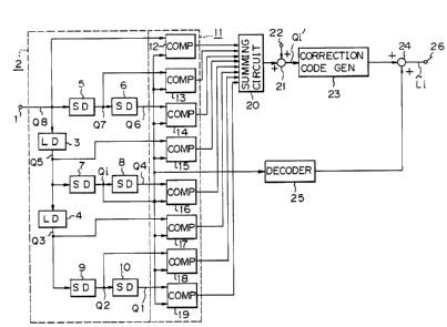
1334691
Input data from an input terminal 1 are received in
the order of television scanning.
An encoded code of two bits received at the input
terminal 1 is supplied to a peripheral data fetching
circuit 2 shown by a broken line. This fetching circuit 2
comprises: line delay circuits 3 and 4; and sample delay
circuits 5, 6, 7, 8, 9 and 10 connected to the input
terminal 1 and respective output terminals of the line
delay circuits 3 and 4.
Said circuit 2 is a circuit to simultaneously fetch an
encoded code Qi of an objective pixel indicated by a black
dot and encoded codes Q1 to Q8 of eight peripheral pixels
of the objective pixel in Fig. 2A. Namely, when the
encoded code Q8 is supplied to the input terminal l, the Qs
is output from the line delay circuit 3, the Q3 is output
from the line delay circuit 4, the Q7 and Q6 are output
from the sample delay circuits 5 and 6, the Qi and Q4 are
output from the sample delay 7 and 8, and the Q2 and Q1 are
output from the sample delay circuits 9 and 10.
The output data from the peripheral data fetching
circuit 2 are supplied to a comparator 11 shown by broken
line. Eight comparators 12 to 19 are included in the
comparator 11. The encoded codes Q8 to Q1 of the
peripheral pixels from the fetching circuit 2 are supplied
to the comparators 12 to 19, respectively, and the encoded
code Qi of the objective pixel is also commonly supplied
thereto.
The comparators 12 to 19 compare the encoded code Qi
of the objective pixel with the encoded codes Qj (j = 1, 2,
1334691
..., 8) of the peripheral pixels and generate the following
comparison outputs:
when Qj > Qi: +1
when Qj = Qi:
when Qj < Qi: -1
The output signals of the comparator 11 are supplied
to a summing circuit 20 and their outputs are added. For
instance, as shown in Fig. 2B, when the encoded code Qi is
2 = (10) and all of the Q1 to Q8 are 1 = (01), the total
value of the summing circuit 20 becomes -8. On the other
hand, as shown in Fig. 2C, when encoded code Qi is 2 =(10)
and all of the Q1 to Q8 are 3 = (11), the total value of
the circuit 20 becomes +8. As shown in Fig. 3, the total
value has seventeen kinds of values of (-8 to +8).
However, when the Qi = 3 = (11), there are nine kinds (0 to
-8) of distributions of the total values. When the Qi is 0
= t00), there are nine kinds (0 to +8) of distributions of
the total values. Therefore, the total value can take 52
kinds of values as a whole in accordance with the encoded
code Qi Of the objective pixel.
The output signal of the summing circuit 20 is
supplied to an adder 21. The datum of +8 is supplied from
a terminal 22 to the adder 21. Therefore, the total values
of (-8 to +8) are converted into (0 to +16) by the adder
21. The output signal Qi' Of the adder 21 is supplied to a
correction code generator 23. A correction code formed by
the generator 23 is supplied to an adder 24. The dëcoded
'` 13~4691
datum of the encoded data Qi Of the objective pixel is
supplied from a decoder 25 to the adder 24. A decoded balue
Li is fetched to an output terminal 26 of the adder 24.
When the number of bits is two, the decoder 25 is an
ROM (read-only memory) or a multiplying circuit to perform
the decoding by a process of (256/22 x Qi). Therefore, the
output value of the decoder 25 is set at (0, 64, 128, 192).
The correction code generator 23 is an ROM or an
arithmetic circuit to generate a correction code from the
output signal Qi' of the adder 21 by the following process.
256 x ~;~ + 0.5) + 0 5
22 X 17
From the value of the above equation, the correction
code of an integer is generated by a discarding process.
When the total value becomes +8 as shown in the example of
Fig. 2C, the output Qi' Of the adder 21 is set to +16.
The correction code generator 23 generates the correction
code of the value of 62. Thus, a decoded value Li which is
obtained from the adder 24 becomes (128 + 62 = 190). As
shown in the example of Fig. 2B when the total value
becomes -8, the output Qi'of the adder 21 is set to 0 and
the correction code generator 23 generates the correction
code of the value of 2. Thus, the decoded value Li which
is derived from the adder 24 is set to (128 + 2 = 130).
Although conventionally represented merely by central
value (e.g., 160), the level is converted into 17 kinds of
1334691
fine reconstruction levels Li on the basis of the values of
the encoded codes of the peripheral pixel as shown in the
foregoing example. Thus, the quantization distortion is
reduced.
The present invention can be also applied to a
decoding of the adaptive dynamic range coding ~abbreviated
to an ADRC) in which a picture plane is divided into a
number of blocks ~two-dimensional regions) and the
quantization is executed so as to be adaptive to the
dynamic range of each block.
Next a second embodiment of the present invention will
be explained with reference to the drawings. This
embodiment is the case where the invention is applied to
ADRC in which a video signal is converted into the
construction of a two-dimensional block and-quantized with
two bits in a manner adaptive to the dynamic range of each
block on the transmission side. For facilitating the
understanding, description of the transmission side will be
given referring to Fig. 4.
A digital video signal given to an input terminal 31
is supplied to a block segmentation circuit 32. The
circuit 32 converts the order of the television scanning
into the block order. One block has a two-dimensional area
of ~x pixels x y lines) as shown in Fig. 5. The output
signal of the block segmentation circuit 32 is fed to a
maximum value detector 33 for detecting a maximum MAX for
every block, a minimum value detector 34 for detecting a
minimum value MIN for every block and a delay circuit 35.
6 ~ 1
The detected maximum value MAX and minimum value MIN
are supplied to a subtraction circuit 36. A dynamic range
DR, which is a difference between the MAX and the MIN, is
produced from the circuit 36. The delay circuit 35 delays
data for a period of time necessary for detecting the MAX
and the MIN. The MIN is subtracted from video data at a
subtraction circuit 37 so as to provide a datum PDI with
the MIN subtracted is given to a quantization circuit 38.
The detected dynamic range DR has been supplied to the
circuit 38, which performs a quantization adaptive to the
DR to generate a two-bit encoded code DT. The quantization
circuit 38 is composed of an ROM or an arithmetic circuit.
At the circuit 38, the dynamic range DR is divided
into (22 = 4) as shown in Fig. 6A and said two-bit encoded
code DT is allotted crresponding to a level range where the
datum PDI with the minimum value subtracted belongs to. In
the conventional decoding method of ADRC, the central value
of each level range is decoded as a representative level.
The encoding shown in Fig. 6A is processing indicated by
the following equation when the value of an encoded code DT
obtained corresponding to an original level Li is Qi:
Qi= Li ~ MIN) X 2
~ ' ~
The above processing is for making an integer by
omitting fractions. This is called "non-edge matching
system".
`- 1334691
Also, for the method of quantization, a method in
which the maximum value MAX and the minimum value MIN are
provided as decoded representative levels by the
conventional decoding method as shown in Fig. 6B may be
employed. This is called "edge matching system".
An additional code consisting of the dynamic range DR
and the MIN and the encoded code DT are fed to a frame
segmentation circuit 39, which performs encoding for error
correction and an addition of a synchronization signal.
Transmission data are produced at an output terminal 40 of
the frame segmentation circuit 39.
Fig. 7 shows a structure on the reception decoding
side which receives the above-mentioned transmission data
and decodes it. The present invention is applied to this
reception side. The reception data given at an input
terminal 41 are given to a frame desegmentation or
separation circuit 42 performs the decoding of an error
correction code and provides the minimum value MIN, dynamic
range DR and encoded code DT separately. The MIN and DR
are supplied to memories 43 and 44, respectively.
The encoded code DT is given to a peripheral data
fetching circuit 45 so that encoded codes of plural, for
example, eight peripheral pixels around an objective pixel
can be taken out. The circuit 45 is a circuit for fetching
the encoded code Qi Of the objective pixel shown by a black
dot in Fig. 2A and the encoded codes Q1 to Q8 Of the eight
peripheral pixels simultaneously. The peripheral data
fetching circuit 45 has a memory for the simultaneous
fetching of the encoded codes of the peripheral pixèls.
13
. 133~691
~ata of pixels in the same block with the objective pixel
are taken out as peripheral data. In the case where a
pixel at one end of a block is the objective pixel, encoded
data of peripheral pixels are interpolated by pixels lying
within the same block, since the peripheral pixels are
contained in another block.
Output data from said circuit 45 are supplied to a
comparator 46, which comprises eight comparison circuits.
The encoded codes Ql to Q8 from the circuit 45 and the
encoded code Qi are supplied to the comparison circuits as
shown in the drawing. Each of these circuits generates the
following comparison output by comparing the code Qi and
the code Qj (j = 1, 2, ...,8):
Qj > Qi : +l
Qj = Qi : 0
Qj < Qi : -1
The output signal of the comparator 46 is given to a
summing circuit 47 for an addition of the comparison
outputs. For example, as shown in Fig. 2B, a sum a of the
circuit 47 is -8 when the encoded code Qi is 2 = (10) and
when each of the Ql to Q8 is 1 = (01). Also, when the code
Qi is 2 = (10) and when each of the Ql to Q8 is 3 = (11) as
shown in Fig. 2C, the sum a of the summing circuit 47 is
~8. In other words, the sum a takes 17 kinds of values
ranging from -8 to ~8.
The output signal ~ is supplied to a correction
code generator 48. The generator 48 is composed of an ROM
14
133~691
for performing a division of (~ = ~/17). The correction
code ~ produced at the output of the generator 48 is given
to an adder 49 and added to the encoded code Qi Of the
objective pixel.
The output signal Qi' of the adder 49 is fed to a
decoder 50 to be subjected to decoding process. The
dynamic range DR from a memory 44 has been supplied to the
decoder 50. This decoder 50 provides a decoded level
depending on the output signal Qi' Of the adder 49. The
output signal of the decoder 50 is given to an adder 51.
The adder 51 performs an addition of said output signal of
the decoder 50 and minimum value MIN from a memory 43.
A decoded level Li Of the objective pixel having a
finer level than the conventional decoded level is provided
from the adder 51. The output signal of the adder 51 is
supplied to a block desegmentation or separation circuit 52
in which the order of blocks is converted into that of the
television scanning. The decoded level is taken out at an
output terminal 53 of the block desegmentation circuit 52.
The decoding process in the above-mentioned second
embodiment will be represented by the following equation:
Qi' = Qi + ~ = Qi + (a/17)
~R X (~ ~ 0.5)
~i= 2 ~ M~N
1334691
In the conventional decoding process, the reception
encoded data Qi is employed in place of the Qi' in the
above equation.
As an example, it is assumed that an original level of
the objective pixel is represented by Li = 61 in a block
with MIN = 50 and MAX = 66 as shown in Fig. 8. The
encoding is made as follows:
Qi = (61 - 50) X 2 2
16
According to the conventional decoding process, the
encoded code Qi is decoded as follows:
^ 16 X ~ + 0.5) + 50 = 6~
In this invention, in the case of (a = +8), for
example, the following decoding is done:
Qi' = 2 + (8/17) . 2.47
Li = 16 x (2.47 ~ 0.5) + 50 61
22
Also, in the case of (a = -8), the decoding is done as
follows:
16
1334691
Qi ' = 2 + (-8/17) , 1 . 53
Li= 16 x (1.53 + 0.5) + ~ 58
22
As a result, the decoded level Li according to the
present invention takes finer steps than the conventional
ones.
In the second embodiment, the decoding is carried out
by referring to the only pixels in the same block because
other peripheral pixels become the ones in other blocks
when the decoding of a pixel at one end of a block.
However, there is a disadvantage that the correct decoding
of the pixel at one end of the block cannot be done.
Therefore, in a third embodiment shown in Fig. 9, an
adaptive decoding is done referring to pixels even if these
pixels are present in other blocks in the decoding
operation.
Reception data is supplied through the input terminal
41 to the frame desegmentation circuit 42. Decoding of an
error correction code is carried out at the circuit 42.
The minimum value MIN, the dynamic range DR and the encoded
code DT are produced separately at the frame desegmentation
circuit 42.
The code DT and the dynamic range DR from the circuit
42 are supplied to the decoder 50. The output signal of
the decoder 50 is given to the adder 51. A decoded level
` ,~ 1334691
Li (decoded value) of a pixel produced at the output of the
adder 51 is given in the following equation:
Li= DR X (~ + 0.5) + MIN
Although the decoding is completed by the above-
mentioned processing in the conventional ADRC, a block
desegmentation and a conversion into the television
scanning are performed, a spatial feature is extracted from
the relationship between the decoded value of the objective
pixel and its peripheral pixels, and an adaptive decoding
is carried out in this embodiment.
A decoded value produced at the output of the adder 51
is supplied to the block desegmentation circuit 52. The
block desegmentation circuit 52 converts data arranged in
the order of blocks into the order of TV scanning. The
output of the circuit 52 is supplied to the peripheral data
fetching circuit 45.
At the circuit 45, decoded values of plural peripheral
pixels, for example, eight peripheral pixels around the
objective pixel are taken out. The circuit 45 takes out a
decoded value Li of the objective pixel lndicated in the
black dot in Fig. 2A and decoded values L1 to L8 Of the
eight peripheral pixels around the objective pixel
simultaneously. For this purpose, the peripheral data
fetching circuit 45 is constructed by a memory or a line-
delay circuit and a sample delay circuit.
18
1334691
. .
Output data from the circuit 45 are supplied to the
comparator 46. A quantization step ~ (= DR/22) of each
block from a memory 60 is given to the comparator 46. The
step ~ is generated from the decoder 50. The comparator
comprises eight comparison circuits. Each of these
circuits is supplied with a corresponding one of the
decoded values L1 to L8 of the peripheral pixels from the
circuit 45 and an addition of the decoded value Li Of the
objective pixel and 1/2 ~. Each comparison circuit
compares (Li + 1/2 ~) and each decoded value Lj (j = 1, 2,
...,8) of the peripheral pixels to produce the following
comparison outputs. In this case, when a pixel of a
peripheral block is used as a reference pixel of the
present block, the addition/subtraction of 1/2 ~ is
performed since it is equivalent to the requantization of
the peripheral pixel based on the dynamic range of the
present block and the minimum value.
Lj > Li + 1/2~: +1
Lj = Li + 1/2~: 0
Lj < Li + 1/2~
The output of the comparator 46 is supplied to the
summing circuit 47 for the addition of comparison outputs.
A sum ~ generated from the circuit 47 takes 17 kinds of
values ranging from -8 to +8.
The output signal ~ and the quantization step ~ of
the summing circuit 47 are supplied to the correction code
generator 48. The generator 48 is composed of an ROM or an
arithmetic circuit for performing the division of
1 9
133~691
x ~) + 17}. The correction value ~ produced from the
generator 48 is given to the adder 49 and added to the
encoded code (decoded value) Li Of said objective pixel.
The output signal Li' of the adder 49 is taken out from the
output terminal 53 as a decoded output. The output signal
Li' with the correction value ~ added has finer steps than
those of a decoded value produced from the decoder 50.
The ADRC system shown in each of the above-mentioned
embodiments is intended for the compression in the level
direction. There is a technique called "intra-frame sub-
sampling" for providing better compression in the
combination with the ADRC system. The intra-frame sub-
sampling is a system for thinning out pixel data
periodically, for instance, in a line-quincunx fashion, to
attain the compression in the spatial direction. As a
result, this sub-sampling enables well-balanced compression
in the combination with the compression in the level
direction by the ADRC system.
An example of the intra-frame sub-sampling is shown
in Fig. 10.
As shown in Fig. 10, a method in which a pixel datum
is transmitted every other pixel datum in the horizontal
and vertical directions as indicated at O and pixel data
shown at X are thinned out is generally employed. With
this, when one pixel is represented by eight bits,
transmission data can be compressed to 1/2 because it
becomes equivalent to the case where all the pixels are
transmitted with four bits.
1334~9 1
In this case, the thinned-out pixel datum indicated
at X is reproduced by an interpolation using pixel data
shown at O and adjacent in the right-handed and left-handed
directions to the pixel datum indicated at X and pixel data
shown at O and lying in the upper and lower directions,
because the transmitted pixel data indicated at O make a
line-quincunx fashion.
However, when the pixel datum lying at the X
position has correlation with the pixel data lying in the
upper, lower, left-handed and right-handed directions in
the case of the above-stated sub-sampling in the frame, the
pixel datum at the X position obtained by the interpolation
comes out excellently. In the absence of said correlation,
the pixel datum at the X position cannot be reproduced.
More specifically, referring to Fig. llA when a video
signal gives an abrupt level change as indicated by a solid
line and there is no correlation between the pixel data at
the X and O positions, pixel data produced by the
interpolation takes a level shown ~ in Fig. llB, since
information on the pixel data at the X positions does not
exist. As a result, The pixel data at the X positions
cannot be reproduced. This means that pixels lying on the
line and consisting only of the pixel data at the X
positions as shown at a solid line a of Fig. 10 cannot be
reproduced.
This is because the information in the level
direction of the pixel data at the X positions disappears
to lack the balance in this direction by thinning out the
~` 1334691
pixel data at the X positions with the space compression
based on the sampling in the space.
To solve this disadvantage, the inventor of the
present application has proposed a novel transmission
apparatus capable of performing well-balanced compression
~refer to Japanese Patent Application No. 63-43363).
Fig. 12 shows an embodiment of the transmission
apparatus and Fig. 13 shows a timing chart for describing
the transmission apparatus.
Referring to Fig. 12, a video signal given through
an input terminal 101 is supplied to an A/D (analog to
digital) converter 102 and sampled by a clock CLK1 (Fig.
13A) fed via a terminal 103. The sampled value is
converted to a five-bit datum (pixel datum) in this
embodiment. The five-bit pixel datum DA of the A/D
converter 102 is directly supplied to one input terminal of
a selector 104 and a selector 105 for selecting upper three
bits. Consequently, only the upper three bits of said
datum DA are obtained and given to the other input terminal
of the selector 104. A selection signal SEL is supplied
from a selection signal generator 125 to the selector 104.
A pixel datum is produced from the generator 125 so that a
five-bit datum and a three-bit datum are obtained
alternately in the horizontal direction and in the vertical
direction for transmission from an output terminal 111.
Fig. 14 is an explanatory diagram of output pixel
data. Five-bit pixel data are indicated at O and three-bit
pixel data are indicated at ~. The pixels lying in the
line-quincunx fashion have the same bit number.
22
133~91
Turning back to Fig. 12, the select~on signal
generator 125 is constructed by flip-flops 106 and 107 and
an Exclusive OR circuit 108. The flip-flop 106 is
triggered by the clock CLKl given through the terminal 103
and reset by a signal SH (Fig. 13B) in synchronism with of
the video signal fed through a terminal 109. A signal PT
tFig. 13), which is one-half of the period of the clock
CLKl and reset at the time of the beginning of a horizontal
interval, is produced. The signal PT is supplied to the
Exclusive OR circuit 108.
The flip-flop 107 is triggered by the signal SH and
reset by a signal FL with a field period, which is given
via a terminal 110. As a result, a signal whose state is
inverted in every horizontal interval (Fig. 13D) is
produced to be supplied to the circuit 108. For this
reason, a signal in which the signal PT with its original
phase and the signal PT with its inverted phase appear in
every horizontal interval, that is, the selection signal
SEL (Fig. 13E) is obtained.
For example, if a five-bit pixel datum is provided
from the selector 105 in the presence of "1" of the
selection signal SE and a three-bit pixel datum is given
therefrom in the absence of "1" of the selection signal SE,
transmission data of an array of five-bit pixel data and
three-bit pixel data in a line-quincunx fashion as shown on
a display of Fig. 14 are provided at an output terminal.
Referring to Fig. 15 which shows the decoding side,
the three-bit or five-bit datum is given to a converter 113
I 339 691
composed of a shift register and its peripheral circuits,
for instance.
Meanwhile, a clock CLk2 with a pixel period on the
reception side is supplied to a conversion control signal
generator 116 through a terminal 114, and a signal ID
indicative of the head position of a horizontal interval or
a field is given to the generator 116 though a terminal
115.
In the case of transmission of a digital video
signal, no horizontal or vertical synchronization signal is
sent. However, since the number of pixel samples per
horizontal line is determined depending on a sampling
frequency, the head of data of a horizontal line can be
discriminated to provide the signal ID. Further, by
keeping the signal ID and the clock CLK 2 at a constant
phase relationship, the clock CLK2 can be synchronized with
a pixel datum.
It is to be noted that the signal ID for
discriminating the horizontal interval, field, etc, may be
sent with data.
A conversion control signal corresponding to the
selection signal SEL on the transmission side is developed
based on the signal ID and the clock CLK2.
In the converter 113, when a pixel datum has five
bits, the five-bit datum is directly output to a D/A
converter 117 by said conversion control signal. Also,
when the pixel datum has three bits, the three-bit datum is
shifted so that this datum takes upper three bits of the
five-bit shift register and "O's" are added to lowér two
24
13:~46~1
bits to provide a total of five bits. This five-bit datum
is output to the D/A converter 117. The clock CLK2 is
supplied to the D/A converter 117, and the five-bit pixel
datum is returned to an analog signal so that a demodulated
video signal is produced at an output terminal 118.
Since a pixel datum is sent with five bits or three
bits in the case of Fig. 12, this is equivalent to the case
where all the pixel data are sent with four bits when
viewed on a picture spatially integrated and is almost
equivalent to the case where the eight-bit pixel data in
the prior art shown in Fig. 10 are transmitted by thinning
out into the line-quincunx fashion.
However, the prior art example of Fig. 10 causes a
picture which is not reproduced as mentioned before because
there are pixels which do not send data at all in
consideration of the compression in the spatial direction.
In contrast, pixel data are sent securely in the
above-mentioned transmission apparatus in consideration of
not only the compression in the spatial direction but also
of that in the level direction. Consequently, the
apparatus enables well-balanced compression to eliminate
the disadvantage in the prior art example.
A fourth embodiment shown below is an example in
which the present invention is applied to a reception
apparatus for receiving transmission data from a
transmission apparatus based on the combination of the
above-stated encoding system and the ADRC system.
This transmission apparatus will be explained
referring to Fig.16 first.
1334691
A picture signal from an input terminal 141 is given
to an A/D converter 142, and each pixel is converted into a
datum by a clock signal CLK1 from a terminal 143, for
instance. The datum is supplied to a block segmentation
circuit 144 and divided into block for every small block
two-dimensional small block of 3 lines x 6 pixels, for
example. Data of each block are fed to a minimum
value/maximum value detector 145 to obtain a maximum value
MAX and a minimum value MIN in each block.
Data of each block from the block segmentation
circuit 144 are supplied to a subtraction circuit 147
through a delay circuit 146 for delaying for a period of
delay time in the detector 145. The minimum value MIN in
that block is given to the subtraction circuit 147. The
minimum value MIN is subtracted from each pixel datum in
said block to produce a difference datum ~DATA. The ~DATA
is fed to an adaptive encoder 148. This encoder 148
corresponds to the quantization circuit 38 shown in Fig. 4.
Meanwhile, data of the maximum value MAX and the
minimum value MIN of each block are supplied to a
subtraction circuit 149 serving as a dynamic range
detector, and a dynamic range DR in a block is detected as
MAX-MIN = DR to be given to the adaptive encoder 148. At
the encoder 148, the allocated bit number BITS in the block
is selected depending on the dynamic range inputted, the
difference pixel datum ~DATA from the subtraction circuit
147 is quantized once again into the bit number less than
the original eight bits, for example, into a datum BPL
26
` 1334~91
compressed into two bits, and the datum BPL is produced
from said encoder 148.
The output datum thus obtained is sent to a selector
150. A datum is produced at the selector 150 by a
selection signal SEL from a selection signal generator 151
so that the bit numbers for horizontally and vertically
adjacent pixels are different to be two bits and one bit in
this example. A clock signal CLK1 is fed to the selection
signal generator 151 through the terminal 143, and
information on the time point of the start of a horizontal
interval used in the block segmentation and information on
the time points of the separation in the horizontal and
vertical directions are supplied from the block
segmentation circuit 144. As a result, the selection
signal SEL is developed.
The two-bit pixel datum and one-bit pixel datum, the
dynamic range DR in the block and the minimum value MIN in
the block are given to a frame segmentation circuit 152.
The selection signal SEL from the circuit 151 is supplied
to the circuit 152 and subjected to frame segmentation.
The datum from the frame segmentation circuit 152 is
transmitted via the output terminal.
In this case, a circuit for converting ~DATA into
the two -bit output datum BPL (for example, ROM) and a
circuit for converting ~DATA into a one-bit output datum
BPL (for example, ROM) may be provided at the adaptive
encoder 148, so that the outputs BPL of these circuits may
be selectively output by the selection signal SEL. In this
case, the selector 150 becomes unnecessary but instead, a
1334691
selector for selecting one of said two circuits should be
provided at the output of the encoder 148. Besides the
datum BPL, the dynamic range DR and the maximum value MAX
in the block or the minimum value MIN in the block and said
value MAX may be employed as additional codes to be
transmitted.
Referring to Fig. 17, a reception apparatus for data
from the encoder shown in Fig. 16 is illustrated as a
fourth embodiment of the invention.
The data sent is given to a frame desegmentation
circuit 162 through an input terminal 161. Picture data
from the circuit 162 are supplied to an adaptive decoder
163. The transmitted dynamic range DR in the block is fed
to the decoder 163 from the circuit 162. The allocated bit
number BITS is obtained depending on the dynamic range DR
at the adaptive decoder 163 so that adaptive decoding can
be made using this information BITS.
The minimum value MIN in the block from the frame
desegmentation circuit 162 is supplied to an adder 165.
In this case, means I (for instance, ROM) for
adaptively decoding a two-bit datum and means II (for
example, ROM) for adaptively decoding a one-bit datum are
provided at the adaptive decoder 163. Two bits and one bit
are given to these means I and II as the allocated bit
number BITS.
A signal associated with the selection signal of the
selection circuit 150 on the encoder side is given from the
circuit 162 to a timing signal generator 164. At the
generator 164, a selection control signal in synchronism
28
1~34691
with the transmitted two-bit and one-bit pixel data is
developed. The control signal is given to the decoder 163
to select the means I or the means II. Consequently, the
respective two-bit pixel datum and the one-bit pixel datum
are adaptively so as to produce an eight-bit difference
datum ~DATA* at the adaptive decoder 163. The ~DATA* is
fed to the adder 165 to provide a decoded pixel datum
DATA*. Since the decoded pixel datum is a datum for each
block, block desegmentation is performed at a block
desegmentation circuit 166 so that said pixel datum is
returned to a pixel datum of its original sequence.
A digital video signal from the circuit 166 is
supplied to an adjacent-pixel-adaptive decoder 167. A
dynamic range DR in a block given from the frame
desegmentation circuit 162 is given to the block
desegmentation circuit 168 so that the dynamic range DR is
adjusted to the time sequence of the digital video signal.
In other words, for each pixel data, a dynamic range DR of
the block to which it belongs is given. The dynamic range
DR from the circuit 168 is fed to the decoder 167. This
decoder 167 corrects a pixel datum sent with two bits
referring to pixel data sent with one bit and lying in its
vicinity as mentioned later.
Also, in this example, the pixel datum sent with one
bit is corrected referring to the pixel data in its
neighborhood as mentioned later.
To select correction processing of the two-bit pixel
datum or correction processing of the one-bit pixel datum
in synchronizm with the input pixel data of the adjacent-
29
`- 1334691
pixel-adaptive decoder 167, the conversion control signal
from the timinq signal generator 164 is supplied to the
decoder 167.
Each correction value from the decoder 167 is fed to
a D/A converter 169 and converted into its original analog
signal in response to the clock signal CLK2 from the timing
signal generator 164 to be taken out from an output
terminal 170.
Fig. 18 shows an example of the above-mentioned
adjacent-pixel-adaptive decoder 167. Description of the
circuit 167 will be given referring to Figs. 19 to 21.
Referring to Fig. 18, a pixel datum (eight bits)
from the block desegmentation circuit 166 is supplied to an
extracting circuit 181 for peripheral pixel data. The
circuit 181 is made up of serially coupled delay circuits
811 and 812 each consisting of a memory corresponding to
one line pixel data. In this case, considering the pixel
position of an output pixel datum SA of the delay circuit
811 to be a reference, an input pixel datum SB of the delay
circuit 811 is a datum of the pixel lying just above the
datum SA, an output pixel datum SC of the delay circuit 812
is a datum of the pixel lying just below the datum SA, an
output datum SD lying after one pixel from the datum SC is
data of the pixel adjacent to the datum SA in the left-
handed direction, and a pixel datum SE prior to one pixel
from the input datum SA given from the delay circuit 812 is
a datum of the pixel adjacent to the datum SA in the right-
handed direction.
1~34691
A dynamic range DR in each of divided blocks from
the block desegmentation circuit 168 is supplied to an
adaptive dynamic range generator 182 for each pixel datum.
The generator 182 is constructed by a series circuit of
delay circuits 821 and 822 each consisting of memory of one
line. As the output datum of delay circuits 821, a dynamic
range DRA corresponding to the pixel datum SA is provided
from the generator 182. A dynamic range DRB corresponding
to the pixel datum SB is given as the input datum of the
delay circuit 821 from the generator 182. Similarly, a
dynamic range DRC corresponding to the pixel datum SC is
provided as the output datum of the delay circuit 822, a
dynamic range DRD corresponding to the pixel datum SD is
generated as the output datum lying after one pixel from
the output datum of the delay circuit 821, and as the
output datum lying prior to one pixel of the input datum
from the delay circuit 822, a dynamic range DRE
corresponding to the pixel datum SE is provided,
respectively.
Also, an upper limit/lower limit generator 183
provides an upper limit UQA2 and a lower limit LQA2 in the
range of quantization levels when the pixel datum SA is a
two-bit pixel datum shown at O of Fig. 19. The pixel datum
SA from the extracting circuit 181 and the adaptive dynamic
range DRA are given to the generator 183.
In addition, the upper limit/lower limit generator
184 provides the upper limits U~A1, U~B, U~C, U~D and U~E
of the respective quantization level ranges of the pixel
data SA, SB, SC, SD and SE and the lower limits L~Al,L~B,
31
` 1334691
L~C, L~D and L~E of said ranges when those data are one-bit
pixel data shown at ~ of Fig. 19. The pixel data SA, SB,
SC, SD and SE and the adaptive dynamic ranges DRA, SRB,
DRC,-DRD and DRE from the generator 182 are supplied to the
generator 184.
For example, the development of the upper and lower
limits in the case of the datum BPL encoded by the non-edge
matching technique will be described.
Fig. 20 shows the case of BITS = 2 in the non-edge
matching technique. Fig. 21 shows the case of BITS = 1 in
the same technique and the case of MIN = O, MAX = 4.
As is clear from Figs, 20 and 21, since decoded
values L0, Ll, L2 and L3 are the central values of the
respective quantization level ranges, the upper limit and
the lower limit become the values equal to an addition or
subtraction of the decoded value of its pixel and k = DR x
1/2x where x is a division number of the dynamic range DR.
k = DR X l/2BITs + 1
In the generator 183, a corresponding dynamic range
DRA with respect to the two-bit pixel datum SA from the
delay circuit 821 is given to an arithmetic circuit 831 to
execute a calculation of DRA x 1/8 and provide a value k2.
The value k2 iS supplied to an adder 832 and a subtraction
circuit 833. Meanwhile, the pixel datum SA, which is a
decoded value, from the extraction circuit 181 iS fed to
the adder 832 and the circuit 833. Therefore, the upper
limit I~A2 of the quantization level range on the datum SA
is produced from the adder 832, while its lower limit L~3A2
is given from the subtraction circuit 833. -
't 133~691
Further, in the generator 184, five circuits each
having an arithmetic circuit 841 for dividing a
corresponding dynamic range from the generator 182 by four
and another five circuits each consisting of an adder 842
and a subtraction circuit 843 for performing an addition
and a subtraction between an output kl from the circuit 841
and each pixel data from the circuit 181 are provided
corresponding to the pixel data SA, SB, SC, SD and SE.
Said two circuit groups produce the upper limits U~A1, U~B,
U~C, U~D and U~E and the lower limits L~A1, L~B, L~C, L~D
and L~E, respectively.
Also, in Fig. 18, switching circuits 185B, 185C,
185D and 185 E and 186B, 186C, 186D and 186E are switched
in synchronism with pixels indicated by circles O of Fig.
19 and pixels indicated by triangles ~ by a control signal
from the timing signal generator 164. When the pixel datum
SA is a pixel shown by a circle, the switching is made into
the shown state, whereas when the datum is a pixel shown by
a triangle ~, the switching is done toward the reverse
state with that shown in the drawing. Those switching
circuits 185B to 185E and 186B to 186E provide pixel data
and information on the upper and lower limits selectively.
Specifically, in the switching state shown in the
drawing, the switching circuits 185B, 185C, 185D and 185E
provide the pixel datum SA, the upper limits U~B, U~C, U~D
and U~E and the lower limits L~B, L~C, L~D and L~E,
respectively.
- 133~91
Moreover, the switching circuits 186B, 186C, 186D
and 186E give the pixel datum SA and the upper limits U~A2
and the lower limit L~A2, respectively.
On the other hand, in the reversely switched state
with that shown in the drawing, the switching circuits
185B, 185C, 185D and 185E provide the pixel data SB, SC,
SD and SE, the upper limit U~A1 and the lower limit L~A1,
respectively.
In addition, the switching circuits 186B, 186C,
186D and 186E give the pixel data SB, SC, SD and SE, the
upper limit U~A1 and the lower limit L~A1, respectively.
Decision circuits 187B, 187C, 187D and 187E are made
up of comparators 871B, 871C, 871D and 871E for comparing
the outputs of the switching circuits 185B, 185C, 185D and
185E and information on the upper limits, comparators 872B,
872C, 872D and 872E for comparing said outputs of the
circuits 185B to 185E and information on the lower limits,
and selection signal generators 873B, 873C, 873D and 873E
for generating selection signals SWB, SWC, SWD and SWE for
selectors 188B, 188C,188D and 188E, which will be mentioned
later, in response to the outputs of the above-mentioned
comparators.
The selectors 188B, 188C, 188D and 188E select one
of three data, i.e., a pixel datum, upper limit and lower
limit given from the switching circuits 186B, 186C, 186D
and 186E based on the selection signals provided by the
decision circuits 187B, 187C, 187D and 187E and send the
selected one datum to a weighted mean circuit 189.
34
1334691
The weighted mean circuit 189 adequately performs
the weighting of the outputs of the selectors 188B, 188C,
188D and 188E, calculates the mean value of the weighted
values, and produces the mean value to an output terminal
190 as a correction pixel datum.
Next, an adaptive decoding operation of the above-
mentioned adjacent pixel adaptive decoder will be
explained.
First, description will be given to the case where a
two-bit pixel datum indicated by a circle O in Fig. 19 is
corrected by referring to one-bit pixel data indicated by
triangles ~.
In the following description, the case where the
decoded value of a pixel A at the position indicated with
hatching in a circle sent with two bits is corrected with
pixels b, c, d and e in its vicinity sent with one bit
indicated by triangles ~ is taken as one example. In Fig.
l9, a thin line shows a block dividing line, and in Fig.
l9A, the pixels A, b and d belong to the same block,
whereas the pixels e and c belong to separate blocks.
Now it is considered that the pixel datum SA from
the extracting circuit 181 is a datum of a two-bit pixel A
shown by an circle in Fig. l9A. In this case, the pixel
data SB, SC, SD and SE become the one-bit pixels b, c, d
and e shown by triangles. For convenience of explanation,
it is assumed that these are pixel data Sb, Sc, Sd and Se.
In this state, the switching circuits 185B, 185C,
185D and 185E and 186B, 186C, 186D and 186E are switched
into the state shown in the drawing.
1334691
As a result, at the decision circuit 187B, the
reception pixel datum Sa is compared with the upper limit
U~B of a quantization level range of the datum Sb of the
pixel b and with the lower limit L~B of said range in the
comparators 87 lB and 872B, and decisions are made on:
whether the pixel datum SA lies in the quantization level
range; whether it is larger than the upper limit U~B; and
whether it is smaller than the lower limit L~B. On the
basis of said decisions, the selection signal SWB is
obtained from the selection signal generator 873B. The
reception pixel datum SA is directly given from the
selector 188B by said selection signal SWB when the datum
SA lies in the quantization level range of the datum Sb.
When the datum SA is larger than the upper limit UQB, the
upper limit U~3A2 of a quantization level range of the
reception pixel datum SA is provided from the selector
188B, while the lower limit of said range of the datum SA
is obtained when the datum SA is smaller than the lower
limit L~B .
When the reception pixel datum SA lies outside of
the quantization level range of the pixel datum Sb,
providing the upper limit U~A2 or the lower limit L~A2 of
the quantization level range of the datum SA is because it
is considered that a correction value of the pixel b in the
vicinity of the datum SA lies in the quantization level
range of the datum SA.
Similarly, at the decision circuits 187C, 187D and
187E, the reception pixel datum SA is compared with the
upper limits U~C, U~D and U~E of the quantization level
36
133~691
ranges of the data Sc, Sd and Se of the pixels c, d and e
and their lower limits L~C, L~D and L~3E, and decisions are
made on: whether the datum SA lies in the quantization
level ranges of the data Sc, Sd and Se; whether it is
larger than the upper limits U~C, U~D and U~E; and whether
it is smaller than the lower limits L~C, L~D and L~lE. As
their decision outputs, the selection signals SWC, SWD and
SWE are produced. By these selection signals, the datum SA
itself is obtained from the selectors 188C, 188D and 188E
when the datum SA lies in the quantization level ranges of
the data Sc, Sd and Se. When the datum SA iS greater than
the upper limits U~C, U~D and U~E, the upper limit U~3A2 of
the quantization level range of the datum SA is obtained,
whereas the lower limit L~A2 of the quantization level
range of the datum SA is provided whether the datum is
smaller than the lower limits L~C, L~D and L~3E.
A correction pixel datum thus obtained from the
selectors 188B, 188C, 188D and 188E is supplied to the
weighted mean circuit 189 where a weighted mean is
calculated. As a result, a correction value of the pixel
datum SA is lead from the output terminal 190.
Here, weighting coefficients at the circuit 189 are
selected so that those having strong correlation with the
pixel A are approaching 1 by referring to distances between
the pixel A and the peripheral pixels b, c, d and e, etc.
In this case, if the decoded value of the pixel A is
L3 = 3. 5 in Fig. 20 and the decoded values of its
peripheral pixels b, c, d and e are all Ll = 3 in Fig. 21,
all the outputs of the selectors 188B, 188C, 188D ar~d 188E
37
1334691
assume L3 = 3.5. As a result, the output of the weighted
mean circuit 189 becomes nearly 3.5. If simple mean is
calculated, the correction value is quite equal to 3.5.
Also, when the decoded value of the pixel A is L3 =
3.5 in Fig. 20, the decoded values of the peripheral pixels
b, c and d are L1 = 3 in Fig. 21, the decoded value of the
pixel e is LO = 1 in Fig. 21, the decoded value L3 = 3.5 of
the pixel A is obtained from each of the selectors 188B,
188C and 188D as it is. The lower limit L~A2 = 3 that can
take the decoded value L3 in Fig. 20 is obtained from the
selector 185E in place of the decoded value 1. The
correction value of the decoded value of the pixel A is
(3.5 X 3 + 3)/4 = 3.375.
Next, it is considered that the output pixel datum
of the extracting circuit 181 is a one-bit datum of the
pixel a indicated at ~ with hatching in Fig. 1 9B. In this
case, the pixel data SB, SC, SE and SE of the circuit 181
are two-bit data of its peripheral pixels B, C, D and E in
Fig. l9B. For simplicity of explanation, it is assumed
that a datum of the pixel a and data of the pixels B, C, D
and E are Sa and SB, SC, SD and SE, respectively.
In this state, the switch circuits 185B, 185C, 185D,
185E and 186B, 186C, 186D, 186E are switched in the reverse
state with the state shown in the drawing.
AS a result, at each of the decision circuits 187B,
187C, 187D and 187E, decisions are made on: the levels of
the respective input pixel data SB, SC, SD and SE lie
within a range W of a quantization level of the pixel datum
Sa: whether they have higher than the upper limit U~A1 in
38
1~34691
the range W; and whether they have lower than the lower
limit L~A1 in the range W. On the basis of said decisions,
the selection signal generators 873B, 873C, 873D and 873E
generate the selection signals SWB, SWC, SWD and SWE.
The selectors 188B, 188C, 188D and 188E are
controlled by the selection signals SWB, SWC, SWD and SWE
given from the decision circuits 187B, 187C, 187D and 187E.
When the levels of the input pixel data SB, SC, SD and SE
lie in the range W of the the quantization level of the
pixel datum Sa, the input pixel data SB, SC, SD and SE are
directly obtained from the selectors 188B, 188C, 188D and
188E. Also, when said levels lie out of the range W and
are larger than the upper limit U~A1, this limit U~A1 is
given from the selectors 188B, 188C, 188D and 188E, whereas
when said levels lie out of the range W and are smaller
than the lower limit L~A1, this lower limit L~A1 is
provided from the selectors 188B, 188C, 188D and 188E.
The outputs of these selectors are supplied to the
weighted mean circuit 189. In a manner similar to that
mentioned above, this circuit performs the weighting of the
outputs of the selectors 188B, 188C, 188D and 188E and
produces their average value by calculation in
consideration of the strength of correlation between the
pixel a and its neighboring pixels B, C, D and E. In this
way, the correction datum of the pixel a is provided from
said circuit 189.
In this case, when the decoded value of the pixel a
is L1 = 3 in Fig. 21 and each of the decoded values of its
peripheral pixels B, C, D and E is L3 = 3.5 in Fig. 20, all
39
13~1691
the outputs of the selectors 188B, 188C, 188D and 188E
assume L3. As a result, the output of the weighted mean
circuit 189 almost becomes L3 = 3.5. With simple mean, the
correction value becomes 3.5.
Further, when the decoded value of the pixel a is L1
= 3 in Fig. 21, each of the decoded values of the pixels B,
C and D among the peripheral pixels is L3 = 3.5 and the
decoded value of the pixel E is L0 = 0.5 in Fig. 20, the
selectors 188B, 188C and 188D give the decoded values L3 =
3.5 directly. The selector 188E provides the lower limit
L~Al = 2 which can take the decoded value L1 in Fig. 21, in
place of the decoded value 0.5. This is because it is
considered that the decoded value of the pixel a exists
only in the quantization level range of the decoded value
Ll when the decoded value of the pixel a is Ll. At this
time, the correction value of the decoded value of the
pixel a is (3.5 x 3 + 2)/4 = 3.125.
Similarly, when the decoded value of a pixel a is L0
= 1 as shown in Fig. 21 and when any one of the peripheral
pixels B, C, D and E is larger than the upper limit of the
decoded value L0, the maximum value existing as decoded
values of the pixel a, that is, the upper limit U~A1 of its
quantization level range is used in place of the decoded
values of the pixels B, C, D and E.
Although the foregoing is directed to the non-edge
matching case, the values k2 and kl can be produced by
calculating an operation of DR x 1/(2BITS + 1 -2) in the
arithmetic circuits 831 and 841 of the upper limit/lower
limit generators 183 and 184 in the edge matching case. In
p 1334691
this case, if the decoded value is the maximum value MAX or
the minimum value MIN, the upper limit and the lower limit
are likely to be larger than MAX by kl or k2 or smaller
than MIN by kl or k2 when these upper limit and lower limit
are obtained by an addition or subtraction between said
decoded value and kl or k2. For this reason, the
generators 183 and 184 produce said MAX and MIN as the
upper limit and the lower limit when the decoded value is
the MAX and MIN. At this time, the MIN is provided by the
block desegmentation of the minimum value MIN in the block
from the frame desegmentation circuit 162, and the MAX is
given by the sum of the dynamic range DR subjected to block
desegmentation and the minimum value MIN subjected to block
desegmentation.
Although data having a large bit number and data
having a low bit number are sent in a line-quincunx fashion
as shown in Fig. 19 in the above-mentioned embodiments,
they may be transmitted by periodically switching those
data.
Also, the bit number may be changed for every plural
pixels in place of varying said number for every one pixel.
Further, the bit number of one pixel or plural pixels may
by changed for every plural pixels. In addition, three or
more kinds of bit numbers may be selectively used instead
of the above-mentioned two kinds.
Also, only pixels lying at the upper, lower, left-
handed and right-handed portions are referred to as
peripheral pixels in the above embodiments. However, when
pixels having small and large bits in the diagonal
1 3 3 4 6 9 1
direction, a correction value may be obtained by taking the
weighted mean. Even in this case, the weighted mean is
calculated by weighting the pixels in the diagonal
direction in consideration of the distances between these
pixels in the diagonal direction and the objective pixel to
be corrected and so on.
According to the present embodiment, in the
reception of a digital video signal transmitted in the
well-balanced compression in the space direction and in the
level direction, a pixel datum with a large bit number is
decoded referring to pixel data lying in its neighborhood
and having small bit numbers. As a result, noises
appearing on a picture due to a difference of bit numbers
are subdued to provide an exellent reception picture.
42