Note: Descriptions are shown in the official language in which they were submitted.
-
1 334726
This invention relates to an apparatus, such as an
optical printer, for optically writing information. The
invention also relates to an apparatus, such as an optical
image reader, for optically detecting or reading information.
a~
1 334726 -`-
In the accompanying drawings:
Figure 1 is a schematic view, in longitudinal section,
showing an optical printer embodying the present invention;
Figure 2 is a sectional view taken on lines II-II in
Figure 1;
Figure 3 is a view illustrative of an lens arrangement;
Figure 4 is a schematic view similar to Figure 1 but
showing an optical reader also embodying the present invention;
Figure 5 is a plan view showing a lens array plate
usable in the printer of Figure 1 or the reader of Figure 4;
Figure 6 is a front view of the lens array plate shown
in Figure 5;
Figure 7 is a plan view similar to Figure 5 but showing
another lens array plate;
Figure 8 is a front view of the lens array plate shown
in Figure 7;
Figure 9 is a perspective view showing another optical
printer using a modified lens holder;
Figure 10 is a sectional view taken on lines X-X in
Figure 9;
Figure 11 is a sectional view taken on lines XI-XI in
Figure 10;
Figure 12 is a plan view showing a conductor pattern for
the optical printer of Figure 1 or 9;
Figure 13 is an enlarged plan view showing a portion
XIII in Figure 12;
1 334726
Figure 14 is a sectional view taken on lines XIV-XIV in
Figure 13;
Figure 15 is a block diagram showing control circuits
for driving the optical printer of Figure 1 or 10;
Figure 16 is a block diagram representing more details
with respect to each of the circuits shown in Figure 15;
Figure 17 is a circuit diagram showing a gate voltage
setting circuit incorporated in the control circuit shown in
Figure 16;
Figure 18 is a schematic diagram showing how the gate
voltage setting circuit of Figure 17 is used;
Figure 19 is a graph showing the characteristic achieved
by the gate voltage setting circuit of Figure 17;
Figure 20 is a plan view showing a modified conductor
pattern suitable for matrix control of the optical printer
shown in Figure 1 or 10;
Figure 21 is a sectional view taken on lines XXI-XXI in
Figure 20;
Figures 22a and 22b are timing charts for the matrix
control of the optical printer; and
Figure 23 is a schematic view showing an array chip
arrangement according to the prior art.
1 334726
Generally, optical printers include a row of light
emitting diodes (LED) arranged to face a photosensitive drum
in parallel thereto, and a lens system arranged between the
diode row and the drum. The row of diodes, when driven for
lighting, forms a row of luminescent dots in various patterns
depenA;ng on the driving control. The lens system serves to
form an image of the luminescent dot row on the drum in
rotation, thus effecting intended printing in accordance with
the driving control.
Most commonly, the lens system for the optical printer
is constituted by an array of self-focusing microlenses
commercially available for example from NIPPON SHEET GLASS
CO., LTD. The array of self-focusing microlenses is designed
and arranged to form an actual size image of a lllmine~cent dot
row on the photosensitive drum without image inversion. In
other words, the dot image row on the photosensitive drum
exactly corresponds in size and dot arrangement to the actual
ll-m;ne~cent dot row. Therefore, in order to conduct correct
1 334726 .~
printing with high quality, it is necessary to arrange the
LEDs at constant minute spacing throughout the entire length
of the LED row.
As shown in Figure 23 of the accompanying drawings, on
the other hand, the LED row, which can be very long in some
applications, is constituted usually by arranging a plurality
of LED array chips 100 in intimate end-to-end contact with
other other. Each array chip 100 incorporates an array of
LEDs lOOa at constant minute spacing. Thus, the spacing y
between each two adjacent LEDs lOOa within each single array
chip 100 must be exactly equal to the spacing x between two
adjacent end LEDs of two different array chips in order to
make the dot spacing constant over the entire length of the
LED row, as required to ensure high printing quality.
However, it is in fact virtually impossible to satisfy this
spacing requirement for the following reasons.
First, in manufacture of LED array chips, each unit chip
is diced or cut from a long wafer carrying a number of LEDs.
However, inevitable limitations on dicing accuracy result in
that a dot spacing irregularity occurs at the position where
each two adjacent array chip 100 are held in intimate
end-to-end contact. An attempt to increase the dicing
accuracy to an acceptable level, on the other hand, will lead
to an unacceptable cost increase.
Second, a similar spacing irregularity also occurs due
to mounting errors in bonding the array chips onto a
substrate. Further, mounting the array chips in intimate
end-to-end contact inheretly involves the risk of arrangement
1 334726
disorder, chip damaging and chip contamination.
In this way, the prior art optical printer incorporating
the row of constantly spaced LEDs and the array of
self-focusing microlenses is disadvantageous in the difficulty
of ensuring high printing quality. Further, the prior art
printer is also disadvantageous in that the self-focusing
microlens array is relatively expensive.
Obviously, the problems discussed above hold with
respect to conventional optical image sensors or readers
wherein a plurality of sensor array chips are arranged in a
row so that all image sensing elements (light receiving
elements) are constantly spaced over the entire length of the
chip row.
1 334726
According to one aspect of the present invention, there
is provided an apparatus for optically writing information
comprising: at least one row of LED array chips arranged as
spaced from each other along the chip row, each array chip
including a plurality of light emitting diodes constantly
spaced along the chip row to provide luminescent dots; a
photosensitive surface arranged in facing relation to the row
of LED array chips in parallel thereto; and a lens system
disposed between the photosensitive surface and the row of LED
array chips, the lens system including a row of convex lens
elements arranged in corresponding relation to the row of LED
array chips, the distance between the row of convex lens
elements and the row of LED array chips being larger than the
focal length (f) of each lens element but less than double the
focal length so that images of the ll~r;n~cent dots of each
LED array chip are formed on the photosensitive surface in an
inverted and magnified arragement, the magnification of the
respective convex lens elements being such that all of the dot
images on the photosensitive surface are constantly spaced
without image overlapping.
According to another aspect of the present invention,
there is provided an apparatus for optically detecting
information comprising: at least one row of sensor array chips
arranged as spaced from each other along the chip row, each
array chip including a plurality of light receiving elements
-- 1 334726
constantly spaced along the chip row; an image surface
arranged in facing relation to the row of sensor array chips
in parallel thereto, the image surface providing an overall
effective width divided into unit array width portions which
correspond in number to the sensor array chips and are
constantly spaced from each other, each unit width portion
containing picture element width portions which are arranged
at a constant pitch and correspond in number to the light
receiving elements of the corresponding sensor array chip, the
pitch being equal to the spacing between the unit width
portions; and a lens system disposed between the image surface
and the row of sensor array chips, the lens system including a
row of convex lens elements arranged in corresponding relation
to the row of sensor array chips, the distance between the row
of convex lens elements and the row of sensor array chips
being larger than the focal length (f) of each lens element
but less than double the focal length, each lens element
functioning to provide image reduction and inversion so that
the distance between the farthest picture element width
portions within the corresponding unit array width portion
exactly corresponds to the distance between the farthest light
receiving elements within the corresponding sensor array chip.
The present invention will be more fully understood
from the following detailed description given with
reference to the accompanying drawings.
- ~ 334726
DETAILED DESCRIPTION
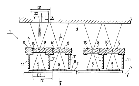
Referring now to Figures 1 and 2 of the accompanying
drawings, there is illustrated an optical printer 1 which
comprises an LED print head 2 arranged in facing relation to a
photosensitive drum 3 in parallel thereto. A lens system 4 is
disposed between the print head and the drum.
The LED print head 2 includes a plurality (e.g. 16) of
LED array chips 5 fixed in a longitl~; n~l row on a substrate 6
as constantly spaced from each other. Each chip 5 comprises a
plurality (e.g. 64 or 128) of light emitting diodes disposed
at constant minute spacing in a longitudinal array on a
strip-form GaAsP wafer of a rectangular cross-section. When
lit, each diode forms a luminescent dot. The print head
further includes a heat sink 7 for preventing excessive
heating of the LED array chip and the substrate.
In manufacture, a single wafer having a large length is
cut into chip lengths by dicing to provide a number of LED
arrays chips at one time.
The spacing between the array chips 5, which is
constant, is determined in dependence on the magnification
provided by the lens system 4. On the other hand, the spacing
between the luminescent dots in each chip 5 is fixed
irrespective of the magnification of the lens system.
The distance between the print head 2 and the drum 3 is
also determined by the characteristic and arrangement of the
lens system 4.
The lens system 4 includes a plurality of convex lenses
8 arranged in exact correspondence with the respective array
1 334726
chips 5. Thus, the pitch between the lenses is exactly the
same as that between the array chips. Each lens may be
aspherical and made of a hard resinous material to have little
or negligible aberration.
The lenses 8 are retained in place by an elongate lens
holder 9 formed with lens holding bores 10 in exact
correspondence with the array chips 5. The lens holder may be
supported at both longitudinal ends (not shown in Figures 1
and 2) on the heat sink 7 in a manner such that the holder is
minutely adjustable in level. The holder may be made either
of a synthetic resin or a metal.
The lens holder 9 is formed with light shielding
partition walls 11 each extending toward a point between two
adjacent array chips 5. Further, the holder has a pair of
light shielding longitudinal walls 12. Thus, each array chip
is substantially enclosed in a box space, so that the light
from that particular chip will not leak into adjacent box
spaces. Such light shielding serves to prevent deterioration
in printing quality.
In accordance with the present invention, the lens
system 4 is arranged so that the distance between each lens 8
and the corresponding array chip 5 (object point) is larger
than the focal length (f) of the lens but smaller than 2f (see
Figure 3). With this arrangement, real images of the
luminescent dots are formed on the opposite side of the lens,
but the image point is located farther from the lens than the
object point. In other words, the lens serves to form
magnified images, in inverted arrangement, of the luminescent
-- 10 --
1 334726
dots at the image point. The photosensitive drum 13 is
located so that its image receiving surface is located at the
image point.
As shown in Figure 1, the pitch between two adjacent
chips 5 is represented as D1, whereas the distance between the
two end dots (farthest dots) in each chip is denoted as D2.
Further, the distance between the two end dot images of the
same chip is represented as D2', whereas the spacing between
two adjacent dot images of the same chip is designated as Y.
Obviously, the distance between the images of two
corresponding dots (correspondingly located or numbered dots)
of two adjacent chips is always equal to D1 regardless of the
magnification provided by the lenses 8. Represented by
reference character X is the spacing between nearest two end
dot images of each two adjacent chips.
According to the present invention, the magnification of
the lenses 8, which is defined as D2'/D2, is set to satisfy
the following equation.
D2'/D2 = (D1-Y)/D2
From the above equation, it is understood that D2'=D1-Y,
so Y=D1-D2'=X. In this way, it is possible to ensure constant
spacing between all dot images even when each two adjacent
chips 5 are reasonably spaced, as illustrated in Figure 1.
The lens holder 9 may be minutely adjusted in level within a
range of allowable image blurring, thereby making the dot
image spacing X exactly equal to Y.
According to the present invention, there is no need to
arrange the respective array chips 5 in end-to-end contact
1 334726
with each other. Therefore, strict dicing accuracy is no
longer called for when manufacturing a number of array chips
from a long wafer. As a result, the dicing step is much more
simplified while drastically increasing the yield of
production. Further, the reasonable spacing between the chips
5 reduces the likelihood of damaging or contaminating contact
between them during chip bonding, thereby facilitating the
bonding operation and ensuring a higher quality of the print
head 2.
The convex lenses 8 can be manufactured at a lower cost
than the self-focusing microlenses which are currently in wide
use. There has been established a technique for accurately
manufacturing aspheric plastic lenses with little aberration.
Thus, it is possible to enhance the quality of the optical
system 4 to a sufficient extent for providing good printing
quality.
The provision of the lens holder 9 having level
adjustability facilitates accurate mounting or positioning of
the lenses 8. Further, the light shielding partition walls ll
serve as reinforcing ribs to prevent deformation of the holder
in addition to preventing light leakage, thereby contributing
greatly to retention of good printing quality.
Figure 4 shows an apparatus for optically reading or
detecting information according to another embodiment of the
present invention. The optical reader l' comprises a reading
head 2' disposed in parallel to an image surface 3' to be
detected. A lens system 4' retained by a lens holder 9' is
arranged between the reading head and the image surface.
1 334726
The reading head 2' includes a plurality (e.g. 16) of
sensor array chips 5' arranged in a longitudinal row on a
substrate 6' as constantly spaced from each other. Each
sensor array chip comprises a plurality (e.g. 64 or 128) of
light receiving elements, such as phototransistors, arranged
at constant minute spacing in an array on a unit wafer which
may be diced from a longer wafer.
The lens holder 9' having lens holding bores 10' and
light shielding partition walls 11' retains aspheric convex
lenses 8' in exactly corresponding relation to the respective
array chips 5'. The arrangement and magnification of the lens
system 4' may be determined in relation to the chips 5' and
the image surface 3' in substantially the same manner as
previously described in connection with the optical printer 1
(Figure 1). However, it should be appreciated here that the
image surface 3' is located at the object point of each lens
8', whereas each chip 5' is located at the image point. Thus,
an image on the surface 3' is reduced when recognized by the
sensor chips 5'.
According to the arrangement shown in Figure 4, the
image surface 3' provides an overall effective width W which
is divided into unit array width portions D2' corresponding in
number to the sensor array chips 5', a constant spacing X
being formed between each two adjacent unit array width
portions D2'. Further, each unit width portion D2' is equally
subdivided into picture element width portions corresponding
in number to the light receiving elements of each sensor array
chip 5'. The pitch Y between each two adjacent picture
- 13 -
I 334726
element width portions is equal to the spacing X described
above. The image reduction provided by each convex lens 8' is
such that the distance between the two farthest picture
element width portions within each unit array width portion
exactly corresponds to the distance between the two farthest
light receiving elements within each sensor array chip 5'.
Thus, by virtue of the image reduction provided by the convex
lens system 4', the entirety of an image or images contained
within the overall effective width W can be scanned at
constant minute pitch Y (equal to X) by the photosensors of
the respective chips 5' even if the chips are longitudinally
spaced as illustrated.
In either of the optical printer l and the optical
reader l', the convex lens system 4, 4' serves to form an
inverted image with respect to each of the respective array
chips 5, 5'. Thus, in order to make a normal printing or
reading, it is necessary to feed serial data or signals to
each chip 5, 5' in reverse order. Such reverse data fee~;ng
will be explained hereinafter in connection with the optical
printer.
In Figures l and 4, the convex lenses 8, 8' are all
separate and individually ret~;ne~ in place by the lens holder
9. Alternatively, a single lens array plate having a required
number of integral lens portions may be used. Further, a
plurality of lens array plates each having a plurality of
integral lens portions may be used in combination to provide a
required number of lens portions.
- 14 -
1 334726
In Figures 5 and 6, there is shown an example of lens
array plate 13. The lens array plate is generally rectangular
in plan view, and has four integral lens portions 13a which
are also rectangular in plan view. The lens portions 13a are
shown as distinctly spaced longitudinally of the plate. The
lens array plate further has a pair of longitudinal margins
13b which are used for mounting purposes, as described later.
Preferably, the lens array plate is made of a plastic.
In assembly, four of such lens array plates 13 for
example are used in combination to provide sixteen lens
portions 13a in total. Alternatively, the lens array plate
may be modified to have sixteen integral lens portions.
Obviously, the use of such a lens array plate or plates
simplifies the construction, and facilitates assembly.
Figures 7 and 8 show another lens array plate 14 which
has three integral lens portions 14a, and a pair of
longitudinal margins 14b for mounting purposes. As opposed to
the example shown in Figure 5, the lens portions 14a have
round configuration in plan view, and merges with each other.
The lens array plate or plates 13 (or 14) described
above may be advantageously held in place by an elongate lens
holder or housing 9" shown in Figures 9 to 11. More
specifically, the lens holder 9" has an upper longitudinal
opening 15 which is rectangular in plan view. The
longitudinal opening 15 is formed with a pair of longitll~;n~l
grooves 15a for receiving the longitudinal margins 13b of the
lens array plate 13. Preferably, the lens array plate or a
terminal lens array plate has an elongated end portion 13c
1 3347~6
which is anchored in a corresponding transverse groove 17 at
each end of the holder. Thus, the lens array plate is
prevented from displacing in any direction relative to the
lens holder.
Above the lens array plate 13 is arranged a transparent
guard plate 18 which is preferably made of an acrylic resin.
The guard plate may be mounted to the lens holder 9" in a
manner similar to the lens array plate. The guard plate
serves to prevent entry of foreign substances such as dust,
thereby protecting the lens array plate and other important
components against contamination and damages.
The lens holder 9" has a lower interior space 19 defined
by a pair of longitudinal walls 12" and a pair of end walls 9a
(only one shown). The interior space is separated by a
plurality of light shielding partition walls 11" extending
transversely of the holder. These partition walls serve to
prevent undesirable light leakage, as already described.
In Figures 9 and 10, the end walls 9a of the lens holder
9" are shown to be supported on the heat sink 7 of the LED
print head 2. Indicated at 20 is a printed circuit board, and
at 21 an electrical connector. The lens holder 9" may be made
of a synthetic resin, whereas the heat sink may be made of a
heat conducting metal such as aluminum. The holder may also
be made of a metal such as aluminum, thereby assisting heat
dissipation provided by the heat sink.
Figures 12 to 14 show a conductor arrangement on the
substrate 6. The conductor arrangement includes a common
cathode strip 22 formed at each end with a terminal lead 22a
- 16 -
1 334726
for grounding. Each LED array chip 5 incorporating an array
of light emitting diodes is mounted on the cathode strip 22
with the cathode of each diode held in conduction therewith.
The chip carries anode pads 23 disposed in a staggered
arrangement on both sides of the diode array, each pad being
held in conduction with the anode of a corresponding diode.
Such a staggered arrangement of the anode pads are necessary
because the diode array density is very high.
The conductor arrangement further includes a pattern of
anode leads 24 extending on the substrate 6 for connection to
relevant control circuits IC (Figure 12) which are provided
for separately driving the respective array chips 5. Again
due to the high density of the diode array, the anode leads
have enlarged connection ends 24a located on both sides of the
cathode strip 22. Thus, a half number of the anode leads must
extend under and across the cathode strip 22 with an
insulation layer 25 interposed between the cathode strip and
the anode leads, as better illustrated in Figure 14. The
connection ends of the anode leads are connected to the
respective anode pads 23 through wires 26.
According to the present invention, there is a
sufficient spacing between each two adjacent array chips 5.
Therefore, this spacing can be utilized to branch out, from
the common cathode strip 22, an auxiliary cathode lead 22b for
grounding. According to the prior art wherein all array chips
are disposed in end-to-end contact with each other, it is
difficult to provide such a branching cathode lead because of
densely arranged anode leads hindering to do so.
- 17 -
~ ~3~7~6
The common cathode strip 22 must be made long when a
large number to LED array chips are used to provide a large
printing width. If the cathode strip 22 has no auxiliary
grounding lead, the internal resistance of the cathode strip
becomes non-negligible with respect to those array chips 5
which are located away from the terminal grounding lead 22a.
In some cases, the intermediately positioned array chips may
suffer a brightness drop of 10-20% due to the increased
internal resistance of the cathode strip.
The auxiliary cathode leads 22b serve to prevent a
brightness drop with respect to all array chips 5 by
separately grounding them though shortest possible paths. If
desired, such an auxiliary cathode lead may be provided only
with respect to one array chip 5 which is located farthest
from the terminal cathode lead 22a.
As previously described in connection with Figure 1,
each lens 8 forms an inverted image, on the photosensitive
drum 3, of the luminescent dot arrangement of a corresponding
LED array chip 5. Thus, some measure must be taken to
compensate for such image inversion in order to carry out
correct printing. A first solution is to feed serial control
signals in reverse order to each control circuit IC (Figure
12). A second solution is to feed serial control signals in
normal order to the control circuit wherein the signal series
is registered in reverse order. Figure 15 illustrates the
second solution.
In Figure 15, each LED array chip 5 is shown to
incorporate an array of light emitting diodes L1-L64. Each
- 18 -
1 334726
control circuit IC comprises a shift register SR, a latch
circuit LA and a drive circuit DR. The shift register SR has
memory cells corresponding in number to the diodes of the chip
for receiving a relevant series of data. The latch circuit LA
has latch cells for parallel latching of the registered serial
data upon reception of a latch signal. The drive circuit DR,
which is connected to the anodes of the respective diodes
L1-L64 via the anode leads 24, functions to supply the latched
data to the diodes upon reception of a strobe signal.
According to the arrangement shown in Figure 15, each
shift register SR is oriented reversely to the data
transmitting direction between each two adjacent shift
registers, so that the serial data supplied in normal order
are registered in reverse order. More specifically, the data
transmission between the two adjacent shift registers SR
occurs in the rightward direction in Figure 15, whereas the
data shifting within the single shift register SR occurs in
the leftward direction. For this purpose, the last memory
cell (numbered 64) of the first shift register (the lefthand
register in Figure 15) is connected in series to the first
cell (numbered 1) of the second shift register, and the last
cell of the second shift register is connected in series to
the first cell of the third shift register, such connection
being repeated up to the last shift register (not shown).
By using the control circuit arrangement shown in Figure
15 in combination with the print head 1 shown in Figure 1, it
is possible to conduct correct printing in spite of the image
inversion provided by the convex lens system 4. In so doing,
-- 19 --
1 334726
the serial data input per se may be carried out in normal
order because data reversal is realized by reverse orientation
of the shift register SR within each control circuit IC.
Figure 16 illustrates a more specific circuit
arrangement for each control circuit IC. The shift register
SR of the control circuit is again shown to include memory
cells SR1-SR64 arranged to store, in reverse order, the serial
data supplied in normal order though a data input terminal
DIN, as previously described. The latch circuit LA includes
latch cells LA1-LA64 for parallel latching of the registered
data of the shift register upon feeding of a latch signal
through a latch terminal LIN. It should be noted that the
memorized or latched data are "1" for those cells
corresponding to the LEDs (Figure 15) to be lit, whereas the
data are "0" for those cells corresponding to the LEDs not to
be lit.
According to the example illustrated in Figure 16, the
control circuit DR includes a gate circuit GA, a logic circuit
LG, a drive transistor circuit TR, and a gate voltage setting
circuit 27.
The gate circuit GA comprises AND gates GA1-GA64. When
a strobe signal is fed through a strobe terminal STR, each AND
gate produces a high or low output "1" or "0" depending
respectively on the "1" or "0" state of the corresponding
latch cell.
The logic circuit LG incorporates logic gates LG1-LG64,
whereas the drive transistor circuit comprises MOSFETs (metal
oxide semiconductor field effect transistor) TR1-TR64 whose
- 20 -
I 334726
output terminals D1-D64 are connected to the respective LEDs
L1-L64 (Figure 15). Each logic gate functions to apply a gate
voltage VG to the gate of the corresponding MOSFET in response
to the "1" output from the corresponding AND gate. As a
result, a voltage equal to a difference between the gate
voltage VG and a source voltage VDD is applied across the
MOSFET for activation thereof, thereby lighting the
corresponding LED L1-L64 (Figure 15) for intended printing.
On the other hand, a voltage equivalent to the source voltage
VDD is produced by the logic gate in response to the "O"
output from the AND gate, so that the MOSFET remains inactive.
As is known, the drive current passing through the LEDs
L1-L64 of each array chip 5 (Figure 15) varies depending on
the magnitude of the gate voltage VG and the characteristic of
the corresponding control circuit IC. Thus, in order to
equalize the average brightness of each LED with respect to
all of the array chips 5, it is necessary to adjust the gate
voltage VG separately with respect to all of the control
circuits IC.
A conventional way for such voltage adjustment is to
provide a voltage dividing circuit arranged outside each
control circuit IC for applying an adjusted gate voltage.
More specifically, the voltage dividing circuit enables
voltage adjustment through changing the voltage division`ratio
by selecting resistors to be incorporated into the circuit.
However, according to this manner of voltage adjustment, it is
difficult to minutely adjust the gate voltage because there is
a limitation on the kinds of available resistors. Further,
-` 1 334726
this manner of voltage adjustment is time-taking.
According to the arrangement shown in Figure 16, the
gate voltage setting circuit 27 incorporated into the drive
circuit DR of each control circuit enables minute voltage
adjustment with ease. Figure 17 represents the detailed
arrangement of the gate voltage setting circuit.
As shown in Figure 17, the gate voltage setting circuit
27 comprises a first group of series resistors Ra, Rb, and a
second group of parallel resistors Rl-R7. The resistor Ra in
the first group is connected to the voltage source VDD, and an
intermediate position between the two resistors Ra, Rb is
connected to a terminal GSO. The resistors R1-R7 in the
second group are connected commonly to the resistor Rb in the
first group, but separately to grounding terminals GSl-GS7.
The connection between the first resistor group and the second
resistor group is further connected to the gate voltage supply
terminal VG. Assuming now that the resistivity of the
resistor Rl is taken as R (i.e. Rl = R), the relative
resistivities of the respective resitors may be set as follows.
Ra = 1.6R Rb = 1.9R R1 = l.OR R2 = 1.6R
R3 = 2.2R R4 = 2.8R R5 = 3.4R R6 = 4.OR
R7 = 4.5R
In use, selected three for example of the grounding
terminals GSl-GS7 are commonly grounded through a common
grounding resistor Rc, as illustrated in Figure 17. The gate
voltage terminal VG is connected to the gate input of each
logic gate LG1-LG64.
- 22 -
1 334726
According to the arrangement of Figure 17, the gate
voltage VG is determined by voltage division of the source
voltage VDD which is provided by the first group resistors Ra,
Rb, the selected three of the second group resistors Rl-R7,
and the common grounding resistor Rc. The second group
resistors R1-R7, seven according to the illustrated example,
provide various combinations (thirty five combinations) for
selecting three of them. Thus, it is possible to minutely
adjust the gate voltage VG, thereby enabling all of the
control circuits IC to uniformly drive the respective LED
array chips 5 (Figure 15) even if there are variations in the
characteristic of the individual control circuits. Further,
the gate voltage setting circuit 27 utilizes only a limited
number of second group resistors in an identical arrangement
for each control circuit, but yet provides various resistor
combinations to enable minute voltage adjustment. Apparently,
this is much more advantageous than the prior art which
requires various kinds of resistors for intended adjustment.
Figure 18 shows an example wherein differently selected
three of the grol~n~;ng terminals GSl-GS7 of the respective
control circuits IC are connected to the c~ ~n grolln~;ng
resistor Rc. In this way, the associated LED array chips 5
are controlled so that the average brightness of each array
chip is maintained within a limited range.
Figure 19 shows a diagram which represents the
achievable range of the gate voltage VG by various
combinations of three grounding terminals when the voltage
across the common grounding resistor Rc (Figure 17) is set at
- 23 -
1 334726
0.5V. In Figure 19, the curve A indicates various gate
voltages available when only the resistor Ra of the first
group is made effective, that is, when the terminal GSO is
shorted to the gate voltage terminal VG. On the other hand,
the curve B indicates various gate voltages obtainable when
the two resistors Ra, Rb of the first group are made
effective. It is understood from Figure 19 that the gate
voltage VG may be varied or adjusted minutely within a wide
range of 1.90-2.90V.
Obviously, the second resistor group of the gate voltage
setting circuit 27 may include more or less than seven
parallel resistors. Further, any number of the second group
resistors Rl-R7 may be selected to increase the range of gate
voltage adjustment.
Referring again to Figure 17, each logic gate LG1-LG64
is shown to include a pair of MOS field effect transistors Ta,
Tb which are opposite in polarity. One transistor Ta is
activated to supply the source voltage VDD to the
corresponding MOSFET TR1-TR64 of the drive transistor circuit
when the signal from the corresponding AND gate GA1-GA64 is
high. The other transistor Tb is activated to supply the gate
voltage VG when the signal from the AND gate is low.
Figure 20 shows a modified arrangement wherein all of
the LED array chips 5 are driven in succession by a single
control circuit IC on the basis of time division. This m~nner
of drive control is called "matrix control", and often used
for LED print heads which are incorporated in cheaper printers
not requiring a high printing speed.
- 24 -
1 334726
As shown in Figure 20, the substrate 6 is formed with
separate cathode strips 22' on each of which is mounted a
corresponding LED array chip 5 incorporating an array of light
emitting diodes L1-L64. Each cathode strip 22' has a terminal
lead 22a for grounding. The cathode of each diode is held in
conduction with the cathode strip, whereas the anode of the
diode is held in conduction with an associated anode pad 23.
A pattern of parallel anode leads 24' connected to the
single control circuit IC extends under and across the
respective cathode strips 22' in a manner such that the anode
leads do not intersect with each other, as shown in Figure
20. For this purpose, each anode lead is made to bridge
between two reversely corresponding diodes of each two
adjacent chips 5. For example, the anode lead extending
immediately under the first diode L1 of one chip is made to
extend ;~m^~; ately under the last diode L64 of the next chip.
The anode leads 24' are connected to the anode pads 23'
by wires 26'. An insulating layer 25' is interposed between
the pattern of anode leads and each cathode strip 22', as
better shown in Figure 21.
In the arrangement of Figures 20 and 21, the terminal
leads 22a' of the respective cathode strip 22' can be taken
out without intersecting with the pattern of anode leads 24'
by utilizing chip spacings at an interval of every two chips,
as shown in Figure 20. Further, the sufficient spacing
between each two adjacent chips 5 makes it easier to keep the
cathode strips electrically independent from each other,
thereby enabling the matrix control of the respective chips.
- 25 -
1 334726
The single control circuit IC comprises a shift register
SR, a latch circuit LA, and a drive circuit DR. Contrary to
the example of Figure 15, the shift register SR for the matrix
control may be oriented to store each series of data in the
order as received for an external data feeding circuit.
In operation according to the matrix control, each
series of data is fed in the shift register SR in synchronism
with a corresponding series of clock signals, as shown in
Figures 22a and 22b. The thus registered series of data is
latched by the latch circuit LA upon feeding of a latch
signal. Upon feeding of a strobe signal, the latched series
of data is supplied for driving the LEDs L1-L64 of a
particular array chip 5 which is made active by feeding of a
block signal VK.
According to the matrix control, all of the LED array
chips 5 may be driven by successively activating them in timed
relation with feeding of successive series of data. However,
due to the image inversion provided by the convex lens system
4 (Figure l) as well as due to the specific anode lead
connections (causing data inversion at every two chips 5), the
successive series of data must be supplied to the shift
register SR alternately in normal and reverse orders to ensure
correct printing. According to the arrangement shown in
Figure 20, specifically, those series of data for the
odd-numbered chips 5 are supplied to the shift register SR in
reverse order, whereas those data for the even-numbered chips
are supplied in normal order.
- 26 -
1 334726
The supplying of alternately inverted series of data can
be carried out by an external data feeding circuit.
Alternatively, the control circuit IC itself may be modified
to register, alternately in normal and reverse orders,
successive series of data which are always supplied in normal
order.
The present invention being thus described, it is
obvious that the same may be modified in many other ways.
Such variations are not to be regarded as a departure from the
spirit and scope of the invention, and all such modifications
as would be obvious to those skilled in art are intended to be
included within the scope of the followings claims.
- 27 -