Note: Descriptions are shown in the official language in which they were submitted.
1 334830
This invention relates to a color sc~nn;ng system which
converts a color image into electric signals, and more
particularly to a color sc~nn;ng system which can enhance the
quality of a read image.
Fig. 1 is a side view schematically showing a
conventional color scanner for explaining a prior-art
example;
Fig. 2 is a plan view showing an image sensor for use in
the color scanner in Fig. l;
Fig. 3 is an enlarged plan view of the detector area of
the image sensor shown in Fig. 2;
Fig. 4 is an enlarged plan view showing the detector
area in Fig. 3 in more detail in order to explain a prior-art
example;
Fig. 5 is a timing chart showing a method of driving the
image sensor in Fig. 4;
Fig. 6 is a timing chart showing a method of driving the
image sensor in a prior-art system;
Fig. 7 is an explanatory diagram showing the positional
relationships between the image sensor and an original in the
prior-art system;
Fig. 8 is an explanatory diagram showing the
relationships between the storage intervals and output
producing times of the detectors in the prior-art system;
- 1 -
1 334830
Fig. 9 is a block diagram showing a method of converting
colors in the prior-art system;
Fig. 10 is a block diagram showing a color signal
conversion circuit in the first embodiment of this invention;
Fig. 11 is a function table for explaining the
operations of selectors included in the color signal
conversion circuit in Fig. 10;
Fig. 12 is a block diagram showing interpolation means
in the second embodiment of this invention;
Fig. 13 is an enlarged plan view showing the layout of
the detectors of an image sensor for use in the embodiment in
Fig. 12;
Fig. 14 is a block diagram showing a signal processing
portion in the third embodiment of this invention;
Fig. 15 is an explanatory diagram showing the operation
of the signal processing portion in Fig. 14;
Fig. 16 is an enlarged plan view showing the
combinations of detectors which constitute the n-th picture
element;
Fig. 17 is an enlarged plan view of the detector area of
an image sensor in the fourth embodiment of this invention;
Fig. 18 is a timing chart showing a method of driving
the image sensor shown in Fig. 17; and
- la -
1 334830
Fig. 19 is an explanatory diagram showing the positional
relationships between the image sensor and an original in the
fourth embodiment.
Throughout the drawings, the same symbols indicate
S identical or equivalent portions.
Fig. 1 is a schematic side view showing a conventional
color scanner. Referring to the figure, an original 1 is
placed on a platen 2. Arranged under the platen 2 is a
fluorescent lamp 3 which is illumination means for
illuminating the original 1. In addition, a rod lens array 5
which is focusing means for focusing the color image of the
original 1 on an image sensor 4 is arranged near the
fluorescent lamp 3.
In the conventional color scanner constructed as stated
above, the original 1 put on the platen 2 is illuminated by
the fluorescent lamp 3, and the color image of the original 1
is focused into an erect real image with the same size as
that of this color image on the image sensor 4 by the rod
lens array 5. The fluorescent lamp 3, image sensor 4 and rod
lens array 5 are unitarily moved relative to the original 1
and platen 2 in the direction of arrow A. Therefore, the
image information
- lb -
1 334830
items of the original 1 are converted into electric
signals sequentially every scanning line.
Figs. 2 and 3 are a plan view of the image
sensor 4, and a plan view showing the layout of
color filters in the photodetective area of the
image sensor 4, respectively. In Fig. 2, the image
sensor 4 is configured of an insulator substrate
41, and a plurality of CCD (charge-coupled device)
image sensors 42 which are disposed straight on
the insulator substrate 41. In Fig. 3, one picture
element 43 is composed of detectors 431 - 434 which
are disposed on one CCD image sensor 42. The detector
431 is a detector which has no color filter (W),
and the detectors 432, 433 and 434 are detectors
whose front surfaces are formed with the color
filters of yellow (Y), green (G) and cyan (C), respectively.
Light having fallen on the detectors 431 - 434
is converted into electrlc signals, whlch are
externally derived by CCD channels (not shown)
disposed on both the sides of the detector array.
Now, there will be explained a method by
which output values derived as stated above are
converted into (R, G, B) values being ordinary
color signals. When Anw, Any, Ang and Anc are
respectively let denote the output values of digital
1 334830
signals obtained by the A/D (analog-to-digital)
conversion of the output signals from the detectors
431 - 434 constituting the n-th picture element
43, the (R, G, B) values are given by the following
equation (1):
~R ~ / 11 M12 M13M14~/Anw ~
G ¦ =M21 M22 M23M24 Any (1)
\ B/ \M31 M32 M3334 Ang
~ Anc/
The matrix of 3 rows and 4 columns used in Eq. (1)
is called a "transformation matrix M", which has
the following elements by way of example:
/1 0 0 --1 ~
M = ~ O 0 1 0 / (2)
\1 --1 0 0 /
Next, operations in the prior-art color filter
array will be explained. Assuming by way of example
that light of yellow whose magnitude is "2" has
entered one picture element 43, the output values
Anw, Any, Ang and Anc of the respective detectors
431 - 434 within the picture element 43 become:
Anw = 2, Any = 2, Ang = 1, Anc =
By substituting these values into Eqs. (1) and
(2), the R, G and B values are obtained as follows:
R = 1, G = 1, B = O
-
1 334830
and it is found that the color of the light having
entered the picture element 43 is yellow.
However, the image of the original 1 is not
limited to one sort of color, but it has the boundary
of colors without fail. How the R, G and B values
are on this occasion, will be explained on a case
where the boundary of colors lies substantially
in the middle of the picture element (at a line
L in Fig. 3). Assuming by way of example that
light of white having a magnitude of "3" has entered
the detectors 431 and 433 and that light of black
having a magnitude of "O" has entered the detectors
432 and 434, the output values Anw, Any, Ang and
Anc of the respective detectors 431 - 434 become:
Anw = 3, Any = O, Ang = 1, Anc = O
In accordance with Eqs. (1) and (2), the R, G and
B values are calculated as follows:
Rn = 3, Gn = 1, Bn = 3
These values indicate a color of magenta group,
and it is understood that noise develops in which magenta
mixes on the boundary line between white and black.
As stated above, the color scanning system
in the prior art has had the problem that, in such
a case where the boundary part of colors on the
original 1 comes to lie in the middle of one picture
t 334830
element 43 in the operation of reading a color
image, the photoelectric conversion outputs of
the picture element 43 exhibit a color quite different
from the colors of the original 1, to incur noise
in the contour part of a read image.
For the purpose of reducing the aforementioned
noise, it is sometimes practised to make the start
times of the storage periods of the CCD image sensor
different and to provide buffer memory circuits
which compensate the attendant shifts of the output
signals. This measure will now be explained with
reference to Fig. 4 thru Fig. 9.
In Fig. 4 which is a more detailed layout plan correspond-
ing to Fig. 3, numerals 141 and 142 designate transfer
gates through which charges generated by input
light in the detectors 431, 432 and the detectors
433, 434 are respectively transferred to CCD channels
151 and 152.
In addition, Fig. 5 is a timing chart showing
the conventional operation of the CCD image sensor 42.
The CCD image sensor 42 operates as follows:
When the transfer gate 141 is in its "off" state,
the light entering the detectors 431, 432 is converted
into the charges, which are stored in these detectors.
Subsequently, when the transfer gate 141 falls
1 334830
into its "on" state, the stored charges are transferred
to the CCD channel 151. Potential wells (not shown)
corresponding to the individual detectors 431, 432
exist in the CCD channel 151. By impressing two-phase
clock pulses 01 and 02 on the CCD channel 151, the
charges transferred thereto from the detectors are
successively shifted to the adjacent potential wells
until they are derived as analog signals out of
the CCD image sensor 42 by a floating diffusion
amplifier (not shown) provided at the final stage
of the CCD channel 151. In actuality, as illustrated
in the timing chart of Fig. 5, transfer gate pulses
0T are input at a period of a time TS (Fig. 5; (a))
while the two-phase clock pulses 01 and 02 (Fig. 5,
(b) and (c)) are being continuously impressed. In
this case, the charges transferred to the CCD channel
151 by the second transfer gate pulse 0T are equal
to the charges stored in the detectors 431, 432
during the preceding time TS. Accordingly, signals
whose magnitudes are proportional to the quantities
of the light having entered the detector 431 formed
with no color filter and the detector 432 formed
with the yellow color filter can be alternately
derived as time series signals from the floating
diffusion amplifier at the final stage of the CCD
1 334830
channel 151. The operations of the detectors 433,
434, transfer gate 142 and CCD channel 152 on the
other side are similar to the operations stated
above.
In a prior-art example, the method of preventing
the noise at the boundary part of the read image
proceeds as stated below:
Symbols 01 and 02 shown at (a) and (b) in
Fig. 6 denote two-phase clock pulses which are
normally and continuously impressed on the CCD
channels 151 and 152 in Fig. 4. Symbols 0TGA and
0TGB shown at (c) and (d) in Fig. 6 denote transfer
gate pulses which are impressed on the transfer
gates 142 and 141, respectively. The periods TSA
and TSB of the respective transfer gate pulses
0TGA and 0TGB become storage times. When the lower
part of Fig. 4 with respect to a center line L'
is defined as channel-A and the upper part as channel-B,
it can be said that the storage time of the channel-A
is the time TSA, while the storage time of the
channel-B is the time TSB. In this prior-art example,
the periods TSA and TSB are equal, but the start
times of the storage times of the individual channels
differ by a time interval TD. As shown at (e)
and (f) in Fig. 6, accordingly, output signals
1 334830
DA and DB from the channel-A and channel-B are respectively
delivered in the order of signals A1g, A1c, A2g, A2c,
... and in the order of signals A1w, A1y, A2w, A2y,
... immediately after the impressions of the transfer
gate pulses 0TGA and 0TGB.
Next, the operation of the color boundary
part will be explained. Fig. 7 shows those positions
(in a vertical line scan direction) of the original
1 (in Fig. 1) at which the detectors of the channel-A
and channel-B in the color scanner exist with the
lapse of time. Letter P in Fig. 7 designates a
vertical line scan pitch. It is assumed that, at
a point of time to indicated in Fig. 7, the detectors
433, 434 of the channel-A lie at a position yO,
while the detectors 431, 432 of the channel-B lie
at a position yO - (P/2). In the color scanner,
the individual detectors 431 - 434 are moved relative
to the original 1. A line S1 in Fig. 7 indicates
the moved states of the detectors 433, 434 of the
channel-A, and a line S2 the moved states of the
detectors 431, 432 of the channel-B. When the
storage time is started at the point of time to~
light which enters the detectors 433, 434 of the
channel-A during the storage time TSA is the reflected
~lght of a part from the position yO to a position yO + P
1 334830
on the surface of the original 1. The detectors
431, 432 of the B-channel photoelectrically convert
the image of a part from the position yO - (P/2)
to a position yO + (P/2) on the surface of the
original 1. This operation has been the major
cause of the generation of the noise at the color
boundary part. Therefore, the start time of the
storage time TSB of the channel-B is set at to + (TSA/2).
Thus, the part from the position yO to the position
yO + P on the surface of the original 1 can be
photoelectrically converted also for the channel-B
as seen from Fig. 7. Accordingly, even when the
color boundary part of the original 1 lies between
the positions yO and yO + P, merely the neutral
tint of the colors on both the sides of the boundary
appears, and no noise can be formed.
The output signals of the individual channels
delivered from the CCD image sensor 42 in this
way are process as stated below: Fig. 8 is a timing
chart showing the storage times TSA, TSB of the
respective channels and the timings of the deliveries
of the output signals DA, DB.
The respective output signals DA, DB begin
to be successively delivered immediately after
the corresponding storage times have ended. In
- 9 -
1 334830
Fig. 8, the delivery intervals of the output signals
DA, DB are indicated by hatched lines. The picture
element signals of the picture elements G, C of
the output signal DA and those of the picture elements
W, Y of the output signal DB shift by a time interval
TD. In converting the output signals into the
(R, G, B) values on the basis of Eq. (1) stated
before, therefore, it is necessitated that the
output signal DA is delayed for the time interval
TD into a signal DA' as illustrated in Fig. 8,
whereupon Eq. (1) is calculated using the signals
DA' and DB.
Fig. 9 is a fundamental block diagram of a
color conversion circuit which converts the picture
element signals G, C, W and Y into the R, G and
B values. The output signal DA delivered from the CCD channel
151 as shown at (d) in Fig. 5 has only its output
signal components sampled and held by a sample-
and-hold circuit 171 in Fig. 9. Thereafter, the
time series signals G and C are separated into
individual signals G and C by a demultiplex circuit
181. Numerals 191 and 192 designate the buffer
memory circuits which serve to delay the respective
individual signals G and C for the time interval
TD. Symbols G' and C' in the figure denote image
-- 1 0
1 334830
signals delayed for the time interval TD with respect
to the respective signals G and C.
The output signal DB delivered from the CCD
channel 152 as shown at (e) in Fig. 5 is similarly
separated into individual signals W and Y through
a sample-and-hold circuit 172 and a demultiplex
circuit 182. The individual signals G', C', W
and Y sampled and held by the above processing
are input to a matrix calculation circuit 110 for
calculating Eq. (1) mentioned before, thereby to
be converted into the R, G and B values.
As thus far explained, the prior-art signal
processing method is such that the start times
of the storage intervals of the respective channels
of the CCD image sensor are made different in order
to reduce the noise of the color boundary part,
and that the attendant shift of the output signals
is compensated by the buffer memory circuits disposed
externally.
Since the prior-art system is constructed
as described above, it requires the buffer memory
circuits which realize the different start times of
the storage intervals of the CCD image sensor for
the purpose of reducing the noise of the color
boundary part and which compensate the attendant
1 334830
shift of the output signals. Therefore, the prior art has
had the problems that the circuit arrangement is complicated
and that the scanner becomes expensive.
This invention provides a color scanning system in which
noise at the color boundary part of a read image can be
reduced by a simple construction.
In one aspect the invention provides a color scanning
system comprises illumination means for illuminating an
original, a plurality of detectors by which a color image
formed by illuminating the original is converted into
electric signals, focusing means for focusing the color image
on said detectors, a plurality of color filters which
discriminate colors of the focused color image and which are
disposed on some of said detectors, and color signal
conversion means; said color signal conversion means
including brightness signal extraction means for setting
signals from the detector with no color filter, as brightness
signals and for deriving the brightness signals corresponding
to (n ~ th, n-th and (n + 1)-th picture elements where n
denotes a plus integer, as brightness signals existing at an
identical time, detection means for detecting differences
between the (n + l)-th and n-th derived brightness signals
and between the n-th and (n - 1)-th derived brightness
signals, interpolation means for interpolatingly processing
color signals of identical color corresponding to the n-th
picture element and the (n - 1)-th or (n + 1)-th picture
element, so as to find a color signal during the meantime,
- 12 -
1 334830
and selection means for delivering one of the n-th color
signal, the (n - 1)-th or (n + l)-th color signal and the
interpolated signal produced by said interpolation means, as
an n-th color signal output in accordance with the detected
difference signals produced by said detection means.
In a further aspect the invention provides a color
sc~nn;ng system comprising illumination means for
illuminating an original, a plurality of detectors by which a
color image formed by illuminating the original is converted
into electric signals, focusing means for focusing the color
image on said detectors, a plurality of sorts of color
filters which discriminate colors of the focused color image
and which are disposed on said detectors, and interpolation
means for imaginarily setting sampling points on the
plurality of detectors and for obtaining individual color
signals at the sampling points through interpolations from
the output signals of said detectors nearby.
In a still further aspect the invention provides a color
scanning system comprising illumination means for
illuminating an original, a plurality of detectors by which a
color image formed by illuminating the original is scanned
and is converted into electric signals, focusing means for
focusing the color image on said detectors, N color filters
(where N denotes an integer of at least 3) which discriminate
colors of the focused color image and which are disposed on
said detectors, comparison means for comparing for one
particular picture element provided with at least one color
filter in each of the respective colors and composed of the M
detectors (where >= N holds) adjacent to one another,
-
1 334830
brightness signals of a plurality of picture elements near
the particular picture element, and selection means for
selecting said M detectors constitutive of the particular
picture element and deciding the colors of the particular
picture element on the basis of signals from said comparison
means.
The invention also provides in a color scanner having a
plurality of detectors which convert a color image into
electric signals, and focusing means for focusing the image
of an original on the detectors, wherein the detectors are
arrayed in a plurality of rows, and the detectors in the
respective rows start accumulating charges generated by
incident light, at points of time different from each other
and accumulate the charges for predetermined accumulation
times, the accumulated charges being delivered as outputs; a
color scanning system characterized in that the accumulated
charges are kept stored in storage means till a predetermined
output time point, whereby output start time points of the
charges accumulated in said detectors of said respective rows
can be set identical.
.,
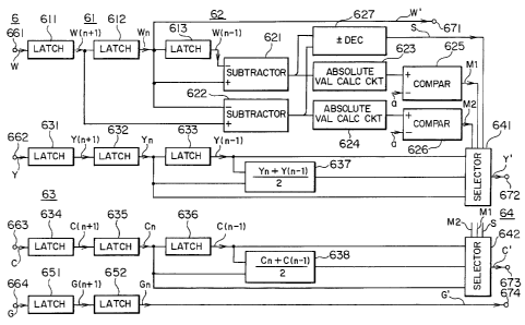
1 334830
Now, the first embodiment of this invention will be
described with reference to the drawings. Fig. 10 is a block
diagram showing a color signal conversion circuit which is
the signal processing portion of a color scanning system
according to
- 15 -
1 334830
this embodiment. The color signal conversion circuit
generally indicated by numeral 6 constructs color
signal conversion means. This color signal conversion
circuit 6 is configured of latches 611 - 613 which
constitute brightness signal extraction means 61;
subtractors 621, 622, absolute value calculation
circuits 623, 624, comparators 625, 626 and a sign
decision circuit 627 which constitute detection
means 62; latches 631 - 636 and interpolation circuits
637, 638 which constitute interpolation means 63;
selectors 641, 642 which constitute selection means
64; and latches 651, 652 which temporarily hold
green (G) signals to delay them. Besides, an input
terminal 661 is supplied with a signal W obtained
by the A/D (analog-to-digital) conversion of a
signal from a detector 431 having no color filter as shown
in Fig. 3, and input terminals 662, 663 and 664
are respectively supplied with signals Y, C and
G similarly obtained by the A/D conversions of
signals from detectors 432, 434 and 433 whose front
surfaces are formed with color filters of yellow
(Y), cyan (C) and green (G). These signals W, Y,
C and G are respectively received in synchronIsm
with unshown reference clock pulses sequentially
from the output of the first detector 431. In
- 16 -
-
1 334830
addition, output terminals 671, 672, 673 and 674
deliver processed color signals W', Y', C' and
G', respectively.
The first embodiment is constructed as stated
above, and the operation thereof will now be described in
detail by referring also to Fig. 11 which is an
explanatory diagram showing the operations of the
selectors 641, 642 of the color signal conversion
circuit 6.
In this embodiment, the signal W from the
detector 431 formed with no color filter is regarded
as a brightness signal. The signals W of the (n ~ th,
n-th and (n + 1)-th picture elements applied to
the input terminal 661 become signals W(n - 1),
Wn and W(n + 1) existing at the same point of time,
through the latches 611 - 613. These signals W(n - 1),
Wn and W(n + 1) are input to the subtractors 621
and 622. The subtractors 621 and 622 subtract
the input signals, and the former 621 delivers
a subtracted signal Wn - W(n - 1), while the latter
622 delivers a subtracted signal W(n + 1) - Wn.
The sign decision circuit 627 operates as an exclusive-
OR circuit, and it takes out only the most significant
bits of the received subtracted signals Wn - W(n - 1)
and W(n + 1) - Wn and calculates (W(n + 1) - Wn) x (Wn - W(n - 1))
1 334830
so as to deliver the sign of the calculated result
as a signal S. This signal S indicates whether
the brightness signal W of a read image is monotonically
increasing or monotonically decreasing in the vicinity
of the n-th picture element, or whether or not
it has an extreme value. In Fig. 11, the signs
of the signal S are denoted by + and --. On the
other hand, the subtracted signals (W(n -- 1) -- Wn)
and (Wn -- W(n + 1)) which are the outputs from the
corresponding subtractors 621 and 622 are respectively
turned into absolute value signals Iw(n + 1) -- Wn
and ~Wn -- W(n + 1)¦ through the absolute value
calculation circuits 623 and 624. These absolute
value signals are respectively compared with a
predetermined value a by the comparators 625 and
626, the respective output signals M1 and M2 of
which are delivered to both the selectors 641 and 642.
Meanwhile, the signals Y of the (n -- 1)-th, n-th and
-(n + 1)-th picture elements applied from the detector
432 to the input terminal 662 are turned into signals
Y(n -- 1), Yn and Y(n + 1) at the same point of
time through the latches 631 - 633. Owing to the
interpolation circuit 637, an interpolated signal
Yn, (n -- 1) corresponding to (Yn + Y(n -- 1))/2
is obtained and is delivered to the selector 641.
- 18 -
1 334830
This selector 641 selects one of its input signals
Y(n -- 1), (Yn + Y(n -- 1))/2 and Yn in accordance
with the aforementioned signals S, M1 and M2 as
illustrated in Fig. 11, and it delivers the selected
signal as the output signal Y' from the output
terminal 672.
Further, the signals C applied to the input
terminal 663 are processed quite similarly to the
signals Y stated above. The selector 642 selects
one of its input signals C(n -- 1), (Cn + C(n -- 1))/2
and Cn in accordance with the signals S, M1 and
M2 as illustrated in Fig. 11, and it delivers the
selected signal as the output signal C' from the
output terminal 673.
In addition, regarding the signal W received
at the input terminal 661 and the signal G received
at the input terminal 664, the n-th signals are respectively
delivered as the output signals W' and G' from
the output terminals 671 and 674 as they are.
How noise at the contour part of the read
image can be relieved by the color signal conversion
circuit 6, will be described in detail below.
First, there will be elucidated a case where
the contour part of the read image is very acute.
Assuming that, as shown in Fig. 3, the contour
- 19 -
1 334830
part of the read image lies at a position corresponding
to the interstice between the detector of the (n ~ th
picture element and the detector 431 of the n-th
picture element having no color filter, the position
is considered to overlie that detector of the (n - 1)-th
picture element whose surface is formed with the
yellow color filter Y(n - 1). In this case, the
read image does not change greatly between the
positions Wn and W(n + 1). Accordingly, even when
the color signals for the n-th picture element
are set at the signals Wn, Yn, Gn and Cn, the noise
of the contour part does not develop. At this
time, the inputs of the comparators 625 and 626
satisfy the following relations:
¦Wn - W(n - 1)¦ > a (3)
~ W(n + 1) - Wn¦ < a (4)
Therefore, the signal M1 becomes greater, and the
signal M2 becomes smaller, with the result that
the signals Yn and Cn are delivered as the respective output
signals Y' and C' in view of the table of Fig. 11.
Assuming that the contour part of the read
image lies at a position corresponding to the interstice
between the n-th picture element and the detector
of the (n + 1)-th picture element having no color
filter, the position is considered to overlie that
- 20 -
1 334830
detector of the n-th picture element whose surface
is formed with the yellow color filter Yn. On
this occasion, the read image does not change greatly
between the positions W(n - 1) and Wn. Therefore,
when the color signals for the n-th picture element
are set at the signals Wn, Y(n - 1), Gn and C(n - 1),
the noise of the contour part does not develop.
In this case, the inputs of the comparators 625
and 626 satisfy the following relations:
¦Wn - W(n - 1)¦ < a (S)
¦W(n + 1) - wnl > a (6)
Therefore, the signal M1 becomes smaller, and the
signal M2 becomes greater, with the result that
the signals Y(n - 1) and C(n - 1) are respectively
delivered as the output signals Y' and C' in view
of the table of Fig. 11.
Next, there will be elucidated a case where
the contour part of the read image is smooth. In
this case, the color signals do not change greatly
among the (n - 1)-th, n-th and (n + 1)-th picture
elements, and the following relations hold:
¦Wn - W(n - 1)¦ < a (7)
¦W(n + 1) - wnl < a (8)
Accordingly, both the signals M1 and M2 become
smaller. Thus, even when the color signals for
- 21 -
1 334830
the n-th picture elements are set at Wn, Yn, Gn
and Cn, the noise of the contour part does not
develop. When the contour part of the read image
fulfills the following relations:
Wn - W(n - 1)¦ > a (9)
!W(n + 1) - wnl > a (10)
it is considered that the image changes comparatively
greatly in the areas W(n - 1), Y(n - 1), Wn, Yn
and W(n + 1). Accordingly,whether the color signals
for the n-th picture element are set at the signals
Wn, Yn, Gn and Cn or at the signals Wn, Y(n - 1),
Gn and C(n - 1), a color which is not contained
in the original (1 in Fig. 1) appears. Therefore,
as indicated by the case of Fig. 11 where the signal
S is +, the signal M1 is greater and the signal
M2 is greater, the color signals of the n-th picture
element are set at Wn, (Yn + Y(n - 1))/2, Gn and
(Cn + C(n - 1))/2, and the output signals Y' and
C' of the positions Yn and Cn are predicted by
the interpolations and are used as the values of
the n-th picture element. Then, the noise of the
contour part can be reduced.
Besides, although the signal S is usually
"+", it can become "-" in a case where the image
hardly changes and where the signs of the difference
- 22 -
1 334830
signals (W(n + 1) - Wn) and (Wn - W(n - 1)) differ
due to noise, and a case where the image is extraordinarily
fine. The former case may be handled quite similarly
to the case where the signal S is "+". The latter
case is a case where the read limits of the scanner
of the pertinent type are exceeded, so that the
signals Wn, Yn, Gn and Cn are used as the output
signals of the n-th picture element. Since, on
this occasion, the change of one picture element
is concerned, the quality of the read image hardly
changes in itself.
Incidentally, the foregoing embodiment has
exemplified the case where one picture element
is composed of the detectors whose surfaces are
formed with the four kinds of color filters. However,
the combination of the color filters is not restricted
thereto, but the same effects as in the embodiment
are achieved even with color filters of red, green,
blue, etc.
In addition, although the output signal from
the detector having no color filter has been employed
as the brightness signal in the foregoing embodiment,
any of signals (Wn + Gn), (Yn + Cn), Gn, etc. may
well be employed, and the same effects as in the
embodiment are achieved.
- 23 -
1 334830
The second embodiment of this invention to
be described below consists in comprising interpolation
means for imaginarily setting sampling points on
a plurality of detectors and for finding individual
color signals at the sampling points by interpolations
from the output signals of the detectors near them.
Fig. 12 is a block diagram showing the interpolation
means 7 for interpolatingly processing the output
signals of the detectors. Referring to the figure,
the input terminals 711 - 714 of the interplation
means 7 are respectively supplied with digital
signals Aw, Ay, Ag and Ac obtained by the A/D conversions
of the output signals from the detectors 431 - 434
(in Fig. 3). For each of the individual channels
of the digital signals Aw, Ay, Ag and Ac, the interpolation
means 7 comprises in equivalent fashion, latches
72, 73 in each of which the corresponding signal
is once heldj a 3/4 multiplier 74 which multiplies
the signal by 3/4, a 1/4 multiplier 75 which multiplies
the signal by 1/4, and an adder 76. Output signals
Wn, Yn, Gn and Cn in white (W), yellow (Y), green
(G) and cyan (C) are respectively derived from
the output terminals 771, 772, 773 and 774 of the
interpolation means 7.
Fig. 13 is a plan view showing the layout
-- 24 --
1 334830
of color filters on an image sensor 4 (in Fig. 1)
likewise to Fig. 3. The detectors 431 - 434 in
Fig. 13 are disposed on the CCD image sensor 42
(in Fig. 2). The detector 431 has no color filter,
whereas the other detectors 432 - 434 are respectively
formed with the color filters of yellow, green
and cyan at the front surfaces thereof. In Fig. 13,
marks o indicate the centers of the respective
detectors 431 - 434, and marks x indicate the imagninary
sampling points.
The second embodiment is constructed as stated
above, and the operation thereof will be described
in detail below. As clarified from the explanation
of the prior-art example, the cause of the noise
at the boundary part of an image lies in the fact
that the detectors shown in Fig. 13, for example,
those 431 - 434, which read the respective color
components perform the photoelectric conversions
of image information items at the different positions
of the original (1 in Fig. 1). Accordingly, the
sampling points are imaginarily set as indicated
by the marks x in Fig. 13, and the signal outputs
of the respective color components at these sampling
points are found by the interpolations of the output
signals from the detectors nearby, whereby the output
1 334830
signals of the image sensor 4 can be given as if
the detectors for the respective color components
lay at the imaginary sampling points at all times.
By way of example, when the imaginary sampling
point n is set at the middle between the detector
431 of area Wn and the detector 432 of area Yn
as shown in Fig. 13, the signals Wn and Yn at the
imaginary sampling point n can be respectively
evaluated by the following equations (11) and (12):
Wn 3 Awn + Aw(n + 1) (11)
Yn = Ay(n 1) + 3 Ayn (12)
Likewise, the signals Gn and Cn at the imaginary
sampling point n at the middle between areas Gn
and Cn can be found by the following calculations:
Gn = 3 Agn + Ag(n + 1) (13)
Cn = Ac(n 1) + 3 Acn (14)
Here, the aforementioned equations (11) - (14)
are realized by the interpolation means 7 of the
embodiment shown in Fig. 12. More specifically, regarding
the output signal Aw from the detector 431 in Fig. 3,
the signal Awn of the n-th picture element and
the signal Aw(n + 1) of the (n + 1)-th picture
-- 26 --
1 334~30
element are obtained at the same point of time
by the latches 72 and 73. Subsequently, the signal
Awn is input to the 3/4 multiplier 74, while the
signal Aw(n + 1) is input to the 1/4 multiplier
75. The processed results of these multipliers
are added by the adder 76, whereby the output signal
Wn is obtained at the output terminal 771. Likewise,
the output signals Yn, Gn and Cn can be respectively
obtained for the input signals Ay, Ag and Ac. Color
signals Rn, Gn and Bn produced by subjecting the
output signals Wn, Yn, Gn and Cn to the transformations
of the following equation afford color image signals
free from the noise at the boundary part of the
image:
/Rn~ ~M11 M12 M13M14\ IWn\
Gn =M21 M22 M23 24 Yn (15)
\ Bn/ ~ 31 M32 M33M341 Gn
~Cn/
Although the foregoing embodiment has been
described as to the case of employing the color
filters of the colors W, Y, G and C and arraying
the detectors in two rows, the colors and layout
of the color filters may well be any others. By
way of example, color filters of colors R, G and
-- 27 --
1 334830
B may well be arrayed in one row, and the same
effects as in the embodiment are achieved.
The third embodiment of this invention to
be described below consists in comprising comparison
means for comparing for a particular picture element,
the brightness signals of a plurality of picture
elements near the particu1ar element, and selection
means for selecting M detectors constitutive of the
particular picture element and deciding the colors
of the particular picture element on the basis
of a signal from the comparison means.
Fig. 14 ls a bloc~ diagram showing a signal
processing portion in this embodiment. The signal
processing portion is configured of at least two
latches 91, 92, two subtractors g3, 94 and two
absolute value circuits 95, 96, and one comparator
97 which constitute comparison means g; and one
selector 90 which constructs selection means. Numerals
911, 912, 913 and 914 designate input terminals
for detected color picture information, which correspond
respectively to white (W), yellow tY~, green tG)
and cyan (C). In addition, numerals 921, 922, 923
and 924 designate output terminals which correspond
respectively to the input terminals 911, 912, 913
and 914. The input terminals 911, 912, 913 and
- 28 -
1 334830
914 are respectively connected to the corresponding
input terminals of the latch 91, and they are collectively
connected to one input terminal of the selector
90. In the latter case, the input terminal of
the selector 90 is supplied with a signal D1 from all
of the input terminals 911 - 914. Besides, a signal
W1 is applied from the input terminal g11 to one
input terminal of the subtractor 93. Similarly, the output
terminals of the latch 91 are ~espectively connected
to the input terminals of the latch 92, and they
are collectively connected to another input terminal
of the selector 90 so as to apply a signal D2 thereto.
Further, the output terminal of the latch 91 corresponding
to white ~W) is connected to the other input terminal
of the subtractor 93 and one input terminal of
the subtractor 94 so as to apply a signal W2 thereto.
~he output terminals of the latch 92 are all connected
to still another input terminal of the selector
90 so as to apply a signal D3 thereto, and the
output terminal thereof corresponding to white
(W) is connected to the other input terminal of
the subtractor 94 so as to apply a signal W3 thereto.
The output terminals of the subtractors 93 and
94 are respectively connected to the absolute value
circuits 95 and g6, the output terminals of which
1 334830
are respectively connected to the input terminals
of the comparator 97. The output terminal of the
comparator 97 is connected to the selector 90. The
absolute value circuits 95 and 96 apply signals
ID1 and ID2 to the comparator 97, respectively,
and the comparator 97 applies a signal SEL to the
selector 90.
This embodiment is constructed as stated above,
and the operation thereof will now be described in
detail with reference to a timing chart in Fig, 15
and a layout plan in Fig. 16 showing detectors
constitutive of picture elements. Signals W, Y,
G and C from the image sensor 4 shown in Fig. 2
etc. are respectively applied to the input terminals
g11, 912, 913 and 914 shown in Fig. 14. As illustrated
at W1 in Fig. 15, the signals W1 of the input terminal
911 are given as Wn-1, Wn, Wn+1, Wn+2, Wn~3 ...
with the lapse of time. Here, letter n denotes
the n-th picture element 43 as shown in Fig. 16.
The signal W1 is changed into the signal W2 as
shown in Fig. 15 by passing it through the latch
91, and the signal W2 is changed into the signal
W~ as shown in Fig. 15 by passing it through the
latch g2. More specifically, letting Wn+1 denote
the white signal W1 applied to the input terminal 911
- 30 -
1 334830
at a point of time tn, the signal W2 ~ecomes Wn
and the signal W3 becomes Wn-1 as indicated in
~ig. 15. These signals are input to the subtractors
93 and 94, the outputs of which are respectively
given as Wn - Wn~1 and Wn - Wn-1. These outputs
are further input to the absolute value circuits
95 and 96, the outputs ID1 and I~2 of which become
ID1 = Iwn - Wn+1¦ and ID2 = Iwn - Wn-1I as indicated
in Fig. 15. The absolute value signals are further
input to the comparator 97 so as to compare the
magnitudes thereof, whereupon a signal Sn is obtained
as the select signal SEL. The signal Sn in this
case is determined by the following conditions:
¦Wn - Wn-1¦ < ¦Wn - Wn+1I (16)
IWn - Wn-1¦ = IWn - Wn~1I (17)
¦Wn - Wn-1I > IWn - Wn+1~
The select signal SEL produced according to these
conditions is sent to the selector 90, and is used
for controlling the selecting operation thereof.
Meanwhile, the collective signal of the signals
W, Y, G and C applied from the image sensor 4 to
the respective input terminals 911, 912, 913 and
g14 become the signal D1 immediately after having
been applie~, the signal D2 after having passed
through the latch 91, and the signal ~3 after having
1 334830
passed through the latch 92, and these signais
D1 - D3 are respectively lnput to the selector
90. The signals ~1, D2 and D3 change as indicated
in Fig. 15 with the lapse of time. At the point
of time tn, they become D1 = Dn+1, D2 = Dn and
D3 = Dn-1 (where Dn denotes the combined output
of white (W), yellow (Y), green (G~ and cyan (C)
of the n-th picture element). According to the
aforementioned conditions of the select signal
SEL and in response to the input signals D1, D2
and D3, the selector 90 delivers the following
outputs Wn', Yn', Gn' and Cn':
~ n' = Wn, Yn~ = Yn-1, Gn' = Gn, Cn' = Cn-1
for Iwn - Wn-1¦ < Iwn - Wn+1I (16);
Wn' = Wn, Yn' = Yn, Gn' = Gn, Cn' = Cn
for Iwn - Wn-1¦ z ¦Wn - Wnl1¦ (11); and
Wn' = Wn+1, Yn ' = Yn, Gn' = Gnl1, Cn' = Cn
for ~Wn - Wn-1¦ > ¦Wn - Wn+1I ~18).
The above results become as shown in Fig. 16
in terms of the combinations of the detectors on
the image sensor 4. In the figure, a part (I)
corresponds to the case of ¦Wn - Wn-1¦ < ¦Wn - Wn~
In this case, the combination 98 of the n-th picture
element is shi~ted in the direction of decreasing
the number n in an amount of one column of the
~ 33~830
detectors relative to the n-th picture element
43 constituting the sensor 4 as shown in Fig. 3.
A part (II) corresponds to the case of ¦Wn - Wn-1¦
= Iwn - Wn+1¦. In this case, the combination 99
of the n-th picture element agrees with the n-th
picture element 43 in the sensor construction. A
part (III) corresponds to the case of ¦Wn - Wn-1¦
> ¦Wn - Wn+1¦. In this case, the combination 100
of the n-th picture element is shifted in the plus
direction in an amount of one column of the detectors
relative to the n-th picture element 43 in the
sensor construction. In a case where the boundary
of colors lies substantially centrally of the picture
element 43, ¦Wn - Wn-1¦ < ¦Wn - Wn+1¦ holds, and
the picture element at this time is composed of
the filter elements (Wn, Yn-1, Gn, Cn-1). Thus,
the noise of the color boundary can be almost eliminated.
In the third embodiment, the latches 91 and
92 have been employed. Since, however, they serve
to delay the image signals, the same effects as
in the embodiment are achieved even when sample-
and-hold circuits or an analog shift register such
as CCD or BB~ are/is used instead.
The fourth embodiment of this invention to
be described below consists in that charges stored
- 33 -
1 334830
in individual detectors are kept stored in storage
means till a predetermined time, whereby the output
start times of the stored charges can be set at
the same point of time.
Fig. 17 shows the construction of the essential
portions of this embodiment.
Numeral 141 designates a transfer gate for
transferring charges generated in detectors 431
and 432 by incident light, to a CCD channel 151.
Numeral 16 designates a line shift gate ~storage
means) for accepting or temporarily storing charges
generated in detectors 433 and 434 by incident
light.
Shown at numeral 142 is a transfer gate for
transferring the charges temporarily stored ln
the line shift gate 16, to a CCD channel 152.
~ ig. 18 is a timing chart showing the setting
of the storage time of each row in the detector
arrayal of two rows as depicted in Fig. 17.
Now, the operation of this embodiment will
be described. Symbols 01 and 02 at ~a) and (b)
in Fig. 18 denote two-phase clock pulses which
are impressed on the CCD channels 151 and 1~2 in
Fig. 17, respectively, and these clock pulses
are applied continuously at all times. Symbol 0V
1 334830
at (c) in Fig. 18 denotes pulses which are impressed
on the line shift gate 16 in Fig. 17. This line
shift gate 16 has potential wells for temporarily
storing the stored charges of the respective detectors
431, 432, 433 and 434. More specifically, when
the line shift pulse 0V is at a high voltage (high
level), the charges of the detectors 433 and 434
are transferred into the line shift gate 16. On
the other hand, when the line shift pulse 0V is
at a low voltage (low level~, the transferred charges
are temporarily stored in the line shift gate 16.
Symbols 0TGA and 0TGB at ~d) and (e) in Fig. 18
denote transfer gate pulses which are impressed
on the transfer gates 142 and 141, respectively.
When the lower part and upper part of the detector
arrayal with respect to a center line ~' indicated
in Fig. 17 are termed channel-A and channel-B, the
storage times TSA and TSB of the channels correspond
to the periods of the pulses 0V and PTG~ in Fig. 18,
respectively.
Next, there will be described how to move
the stored charges of the respective channels shown
in ~ig. 17. The detectors 433 and 434 of the channel-A
in Fig. 17 store the charges generated by the incident
light, during the interval (interval TSA) from
- 35 -
1 3~ 3~
the high level (at a point of time to) to the next
high level (at a point of time t2) of the pulse
0V shown at (c) in Fig. 18. The stored charges
enter the potential wells within the line shlft
gate 16 in Fig. 17 at the point of time t2 so as
to be stored therein. Thereafter, when the pulse
0TGA at (d) in Fig. 18 as impressed on the transfer
gate 142 in Fig. 17 becomes its high level (at
a point of time t3), the charges stored in the
line shift gate 16 are transferred to the CCD channel
152 in Fig. 17, and the transferred charges are
successively delivered as outputs since the point
of time t3.
On the other hand, the detectors 431 and 432
of the channel-B in Fig. 17 store the charges generated
by the incident light, during the interval (interval
TSB) from the high level ~at a point of time t1)
to the next high level (at the point of time t3)
of the pulse ~TGB shown at (e) in Fig. 18. The
stored charges are transferred to the CCD channel
151 through the transfer gate 141 in Fig. 17 at
the point of time t3, and the transferred charges
are successively delivered as outputs since the
point of time t3.
Next, there will be described the operation
- 36 -
1 334830
of this embodiment at a color boundary part. Fig. 19
show those positions (in the direction of vertical
line scan) of an original (1 in Fig. 1) at which
the detectors of the channel-A and channel-B in
the color scanner exist with the lapse of time.
Letter P denotes the pitch of the vertical line
scan. It is assumed that, at a point of time
to indicated in Fig. 19, the detectors 433 and
434 of the channel-A lie at a position yO, while
the detectors 431 and 432 of the channel-s lie
at a position yO -- ~P/2). In the color scanner,
the detectors 431 - 434 are moved relative to the
original 1. Symbol S1 in Fig. 19 denotes the moved
states of the detectors 433 and 434 of the channel-A,
and symbol S2 the moved states of the detectors
431 and 432 of the channel-B.
Points of time to~ t1~ t2 and t3 in Fig. 19
correspond to the points of time indicated by the
same symbols in Fig. 18, respectively.
In this embodiment, the start times of the
storage times TSA and TSB of the respective channels-
A and B are the same as in the prior-art example
stated before. That is, the start time t1 of the
storage time of the channel-B is set at to + (TSA/2).
Thus, noise to develop at the color boundary part
-- 37 -
1 334830
is eliminated as in the prior-art example.
This embodiment is further contrived so that
the charges stored in the channel-A during the
interval TSA may begin to be temporarily stored
in the line shift gate 16 in Fig. 17 at the end
point of time t2 of the storage time TSA and may
begin to be output at the point of time t3 in Fig. 1g.
This point of time t3 is identical to the output
start time of the charges stored in the channel-B.
That is, the char~es stored in both the channels-A
and B during the respective storage times TSA and
TS~ are output at the same point of time.
As thus far described, according to this embodiment,
the buffer memory circuits having hitherto been
required for reducing the noise of the color boundary
part are dispensed with, so that the color scanner
of simple circuit arrangement and low cost can
be provided.
Although the foregoing embodiment has indicated
the case where the storage times TSA and TSB of
the respective channels are equal, they may well
be unequal time intervals. In addition, although
the embodiment has indicated the case where the
detectors 431 - 434 ~re linearly moved relative
to the orlginal 1, the moving method is not restricted thereto.
- 38 -