Note: Descriptions are shown in the official language in which they were submitted.
1335190
In the past few years there has been a tremendous
amount of activity in the area of replacing "subtractive"
printed circuit boards with "additive" printed circuit
boards. There are major environmental, economic, and
marketing reasons for the interest expressed in this
technology. Two of the more important reasons are the
growth of the electronic industry and the environmental
problems associated with traditional copper "substantive"
- circuit boards which consume resources, such as the copper
foil itself, as well as the process itself which generates
hazardous waste.
In an effort to overcome or minimize the
disadvantages associated with the production of
"subtractive" printed circuit boards, membrane switch
circuit boards were developed in the late seventies and
early eighties. These circuit boards were generally silver
loaded resin inks printed on polyester films. However,
they exhibited rather low voltage and current carrying
capabilities and were employed principally in the field of
simple switches and not as true printed circuit boards.
It is also important to distinguish additive
technologies, such as CC-4 boards which rely on
electrodeless copper plating to achieve an additive circuit
board from the present invention. The former, which indeed
is an additive process, nonetheless continues to produce
undesirable effluents even though it offers some cost
advantages over the more conventional subtractive
techniques. On the other hand, the present invention not
only avoids the production of undesirable effluents but
also provides economic advantages over systems heretofore
employed in the production of printed circuit boards.
Two of the more significant advantages secured by
the present invention, not achievable heretofore, are
(1) a low cost silver based ink providing low
resistance values and being W -curable and
1335190
(2) a low cost silver based solderable ink which
also provides low resistance and is W -curable. In both
instances the present invention provides a circuit trace
whose cross-section involves a W -curable material in
combination with either silver coated glass or silver
coated magnetite spheres.
An inherent problem associated with W technology
resides in the fact that the W material itself is non-
conductive and represents a significant percentage of the
conductive ink composition. In many cases this can be as
high as 30% W -curable resin and 70% conductive material.
While the advantages of the present invention are
applicable to planar boards or substrates, it will be
appreciated that these same advantages can be secured with
non-planar substrates such as, for instance computer
keyboards and the like.
The present invention thus relates to systems for
securing the above noted advantages and for avoiding the
disadvantages associated with known methods of producing
printed circuit boards.
One of these systems involves curing the W -
curable resin component of the W -curable ink containing
spherical conductive particles by subjecting the same to a
W source in a pulsing manner.
Another of these systems involves the use of a
magnetic field and while under the influence of the
magnetic field curing the W -curable resin containing
spherical magnetite conductive particles by subjecting the
same to a W source whether or not in a pulsing manner.
Accordingly, one aspect of the invention provides
a method for producing a circuit board having conductive
circuit elements with a specific resistivity of less than
about 0.05 ohm-cm patterned on a non-conductive substrate
comprising:
a. printing a W -curable ink onto the non-
conductive substrate in a desired circuit pattern; and
1335190
b. effecting W radiation cure of the W -curable
ink by exposing said W -curable ink to a W source having
an output of from about 360 nm to 420 nm in a pulsing
manner comprising from 5 to 8 one-half second exposure
periods, each exposure period followed by a non-exposure
period of from about 2 to 3 seconds.
The features and advantages of the present
invention will be more clearly appreciated from the
following description taken in conjunction with the
accompanying drawings in which:
Figure 1 is a schematic cross-section through an
ink film containing conductive spheres, which ink film is
not treated in accordance with the present invention;
Figure 2 is a schematic cross-section through an
ink film also containing conductive spheres, which ink film
has, in accordance with the present invention been
subjected to a W source in a pulsing manner or to a W
source under the influence of a magnetic field whether or
not the W source is applied in a pulsing manner;
Figure 3 is a schematic view illustrating the
packing of identical spheres whereby adjacent layers
thereof are capable of slipping past one another;
Figure 4 is a schematic view illustrating the
packing of identical spheres whereby adjacent layers
thereof are not capable of slipping past one another;
Figure 5 is a schematic view illustrating the
present invention wherein spheres vary in diameter by at
least plus or minus 15 microns thereby permitting
additional packing without undue reduction in fluidity yet
providing high conductivity;
Figure 6 is a schematic of one embodiment of the
magnetic device of the present invention;
Figure 7 appears following Figure 8 and is a
frontal schematic of another embodiment of a magnetic
device of the present invention;
133S19
Figure 8 is a side view of the magnetic device of
Figure 7.
In Figure 1, which illustrates a typical
dispersion of spherical particles 12 in a resin 10, the
problem of having large interstices between the particles
filled with resin which is an insulator can be easily seen.
On the other hand, in Figure 2, which is representative of
the present invention, the spherical particles 12 are
closely packed with only a small amount of resin 10 filling
the interstices therebetween.
General DescriPtion of a First System
The inventor has now discovered that when a W
source with an output of from about 360 nm to 420 nm is
employed in a pulsed mode, a shrinkage of the conductive
ink circuitry film occurs whereby shrinkage is facilitated
evenly throughout the conductive ink film thickness. This
causes the conductive particles to move into closer contact
with regard to one another, thus resulting in the
conductive ink circuitry or trace being capable of carrying
a greater operating current, as well as lowering the
current resistance.
Specific De~cription of the First System
One embodiment of the present invention thus
relates to a method for producing a circuit board having
conductive circuit elements with a specific resistance of
less than about 0.05 ohm-cm patterned on a non-conductive
substrate comprising
(a) printing a W -curable ink onto the non-
conductive substrate in a desired circuit pattern and
(b) effecting a W radiation cure of the W -
curable ink by exposing said W -curable ink to a W source
having an output of from about 360 nm to 420 nm. The
-- 4
- 133~190
exposure of the ink to the W source is effected in a
pulsing manner which comprises from 5 to 8 one-half second
exposure periods, each exposure period being immediately
followed by a non-exposure period of from about 2 to 3
seconds. When the ink is cured in accordance with the
present invention a shrinkage of the ink film thickness
occurs and is facilitated evenly throughout the conductive
ink film thickness. This causes the particles to move into
closer contact with one another, thus resulting in the
patterned conductive circuit elements being capable of
carrying a greater operating current as well as exhibiting
a lower resistance.
The W source employed in the present invention
is electrodeless. Instead of using electrodes to feed
energy into the discharge, the discharge tube absorbs
microwave energy via waveguides into a microwave chamber in
which the tube is housed. The lamp system employed in the
present invention is modular and consists of two parts, an
irradiator and a power supply. The irradiator contains a
microwave chamber formed by an anodized aluminum reflector
of semi-elliptical cross-section with flat ends. The lamp
itself is a closed, 10 inch-long tube of transparent
vitreous silica varying in internal diameter from 8 mm near
the ends to 6 mm at the center. The lamp is located so
that its axis lies at the focus of the ellipse and it acts
as a dissipative load. Microwave energy is generated by
two 1500 watt magnetrons and is fed through waveguides into
the chamber via rectangular slots cut in the back of the
reflector. The microwave frequency used is 2450 MHz. The
magnetrons and waveguides are cooled by a filtered air flow
and this air is also passed through small circular holes
cut in the back of the reflector, and over the lamp. In
order to better disperse the output of the lamp and fully
cure the conductive circuit elements, the surface of the
reflector is provided with 1 inch facets much like the
surface of a golf ball.
133~190
An important factor which dictated the election
of an electrodeless W output source is the lack of lamp
deterioration associated with electrodes. This
deterioration has prevented W resins from being used in a
truly viable production of circuit boards of the type
produced in accordance with the present invention. One
reason for this is that in an electrode lamp the output
wavelength will vary with time due to electrode
deterioration, and there is a direct relationship between
degree of cure of the curable W resin and the current
carrying capability of the conductive circuit elements
produced therefrom. The inventor has found a particularly
effective electrodeless lamp is one with iron iodide as a
dopant which enhances the spectral output in the wavelength
of from about 360 nm to 420 nm.
Suitable substrates on which the W -curable ink
of the present invention can be printed, especially for use
in membrane switches are generally organic polymer films
having the properties of high flexibility, tensile
strength, elasticity, dimensional stability and chemical
inertness. Transparency is also a frequently desired
property for such materials. Materials meeting these
criteria include polyolefins such as polyethylene and
polypropylene, polycarbonates, polyesters and polyvinyl
halides such as polyvinyl chloride and polyvinyl fluoride.
The most highly preferred and most widely used substrate
material for membrane switches is a polyester film, e.g.
Mylar~ polyester film.
The W -curable ink employed in the present
invention comprises from about 33 to 38% by weight of a
thermosetting resin binder and from about 67 to 62% by
weight of spherical or spheroidal conductive particles
having a particle size distribution ranging from about 1 to
30 microns.
Representative thermosetting resins usefully
employed in the present invention include
1335190
(1) phenolic resins such as those produced by
reacting phenols with aldehydes;
(2) amino resins such as the condensation
products of urea and of melamine with formaldehyde;
(3) unsaturated polyester resins wherein the
dibasic acid or the glycol, or both, contain double bonded
carbon atoms as exemplified by the following:
Unsaturated Polyester 8ystems
O
c~_CH2 + ~ 3 ~ c ~
15 1,2-propylene phthalic maleic
glycol anhydride anhydride
1 heat
O ICH3 ~ 1l CIH3 1lICH3 O
OC-eH CH-O-C ~ ~ C-O-fH HC-CO-CH CH-C-O-fH2
HC-CO-CH2 ~ CH2-OC-CH CH2-OC-CH CH-O
o O O CH3
Unsaturated Polyester
Unsaturated acids include maleic anhydride or fumaric acid
while when the unsaturation is supplied by the glycol, a
saturated acid or anhydride such as phthalic anhydride or
adipic, azelaic or isophthalic acid can be employed.
Ethylene and propylene glycols are often employed but 1,3-
and 2,3-butylene, diethylene and dipropylene glycols are
also often used. While styrene is commonly employed, other
monomers used include vinyl toluene, methyl methacrylate,
diallyl phthalate and triallyl cyanurate;
1335190
(4) epoxy resins such as the condensation product
of epichlorohydrin with bisphenol A, although other
hydroxyl-containing compounds such as resorcinol,
hydroquinone, glycols and glycerol can be employed and
(5) silicone polymers produced by intermolecular
condensation of silanols. Other thermosetting resins such
as alkyd resins including those based on phthalic anhydride
and glycerol, or those based on other polyhydric alcohols
such as glycols, pentaerythritol or sorbitol, and other
acids such as maleic anhydride, isophthalic and
terephthalic acid can also be used. Still other
thermosetting resin binders include allyl resins, e.g.
diallyl phthalate and allyl diglycol carbonate, as well as
furane resins such as those based on furfuraldehyde in
combination with phenol.
Preferably, the thermosetting resin binder
employed in the present invention is a formulation of
liquid acrylic modified monomers, oligomers and polymers
activated by a combination of a ketone photo-initiator and
an amine. The resin is synthesized with either a terminal
or pendant acrylate group, with a urethane being the
preferred oligomer, as follows:
Acrylated Polyurethanes
O O CH3 O - - O
Il 11 1 11 11
CH2=CH-CO-CH2CH2-OC-NH ~ NH-C- OCH2CH2- OCNH
H3C NH
CH2=CH--CO--CH2CH2--0--C=O
11
o
Polyethylene Oxide
~,~
1335190
o o o _ _
11 11 1i
CH2=CH-CO-CH2-CH20C-NH ~ NH-C-O -HD-AD -HD
CH3 NH CH3
CH2=CH--CI O--CH2CH2--0--C=O
x
[HD-AD] n Polyester based on Adipic
acid (AD) and hexanediol (HD).
Other suitable resins include acrylated epoxy resins, such
as Novacure~ 3700, available from Interez, Inc., having the
following chemical formula
CH2=CH-CO-CH2-fH-CH2-O ~ ICH3 O-CH2-fH-CH2-O-C-CH=CH,
OH CH3 OH
acrylated polyethers, such as the following polyether based
on 1,2,6-hexane triol and propylene oxide
ICH3 0
CH2 (0CHCH2) nO-C-CH=CH2
fH3 1
7H(OCHCH2)nO-C-CH-CH2
(CH2)3
¦ CH3 O
CH2 (OCHCH2) nO--C--CH=CH2
acrylated polyesters, such as those formed from the
esterification of polyhydric esters with acrylic acid to
yield
...
1335190
o --o o o
11 11 11 11
2 CHC (CH2) 6 (C-cH2) 4-C-O--(CH2) 6--0C-cH=cH2
which specifically is a polyester based upon adipic acid
and hexanediol; and thio/ene and thio/acrylate systems,
such as the polythiols developed by W. Grace and Company,
Ltd., pentaerythritol tetrakis (thioglycolate)
o
Il
CH2-OC-CH2-SH
O O
HS-CH2C-OCH2-C-CH2-O-C-CH2-SH
o
20CH2-O-C-CH2-SH
and trimethylol propane tris (~-mercapto propionate)
ll
CH2-0-C-CH2-SH
H 0
11
30CH3-cH2-c-lH2-o-c-cH2-cH2-sH
CH2-0- IC-CH2-CH2-SH
o
In order to achieve longer wavelength absorption
in the range of from about 360 nm to 420 nm, a ketone amine
adjuvant is employed. Preferably this adjuvant is
Michler's ketone since it contains both ketone and amine
functionality in one molecule. However, a mixture of
benzophenone and Michler's ketone has been found to be
particularly effective
-- 10 --
I335190
(l) where the two components are admixed prior to
incorporation into the curable ink vehicle,
(2) where the spherical or spheroidal conductive
particles are silver coated glass spheres and
5(3) where the latter are present in the W -
curable ink in an amount greater than about 60% by weight
based on the total weight of the curable ink.
The spherical or spheroidal conductive particles
employed in the present invention are preferably, silver
coated glass spheres having the following characteristics:
average particle diameter - about 15 microns;
average particle size distribution - from about
1 to 30 microns;
silver coating - about 12% by weight based on the
total weight of the spheres;
particle density - about 2.7 g/cc;
specific surface area - about 0.178 m /g; and
minimum percent rounds by microscope - about 90.
Other particulate materials such as iron, zinc,
nickel, copper and the like can also be employed, these
particulate materials having a particle size distribution
and an average particle size previously defined.
The output spectra of six electrodeless lamps
were tested and analyzed for their effectiveness in curing
a W -curable ink in accordance with the present invention.
The results are given below.
1335190
- Lamp A Lamp D Lamp M
Interval Power Power Power
(NM)
~w) (acc) (~) (acc) (~) (acc
200-210 7.9 8 7.7 8 13.4 13
210-220 17.0 26 15.2 23 42.4 56
220-230 25.3 51 15.8 39 67.2 123
230-240 23.6 75 14.6 53 46.2 170
240-250 27.6 102 24.8 78 303 200
250-260 55.7 158 43.1 121 101.2 301
260-270 38.9 197 32.1 153 78.1 379
270-280 48.8 246 42.9 196 34.7 414
280-290 91.0 329 24.6 221 28.7 443
290-300 39.3 366 48.6 269 43.5 486
300-310 72.0 73 56.7 57 46.2 46
310-320 77.6 150 44.2 101 92.1 138
320-330 64.5 21S 35.5 136 9.0 147
330-340 25.6 240 20.3 156 18.4 166
340-350 9.3 250 43.2 200 5.4 171
350-360 48.4 298 78.0 279 5.2 176
360-370 58.6 357 93.3 373 118.9 293
370-380 25.2 382 115.2 488 8.0 307
380-390 37.1 419 112.1 600 6.3 310
390-400 11.5 430 41.2 641 5.9 315
400-410 92.9 93 46.9 47 50.5 50
410-420 10.1 103 33.5 80 7.0 57
420-430 15.5 119 44.6 125 7.9 65
430-440 41.0 160 61.7 187 79.5 145
440-450 30.1 190 28.2 215 8.8 154
- 12 -
- - 1335190
- Lamp M' Lamp V Lamp X
Interval Power Power Power
(u) (acc) (u) (acc) (u) (acc
200-210 7.5 7 0.4 0 7.1 7
210-220 20.9 28 1.4 2 22.1 29
220-230 31.4 60 2.9 5 32.3 62
230-240 27.9 88 3.6 8 41.3 103
240-250 29.8 118 7.3 16 34.5 137
250-260 73.1 191 11.5 27 55.7 193
260-270 79.5 270 12.5 40 48.3 241
270-280 31.7 302 12.3 52 29.3 271
280-290 85.1 387 26.2 78 38.2 309
290-300 26.8 414 46.5 125 38.8 348
300-310 20.9 21 16.0 16 29.1 29
310-320 42.5 63 17.3 33 51.4 80
320-330 10.1 74 16.4 50 26.4 107
330-340 10.8 84 20.2 70 25.9 133
340-350 6.9 91 22.3 92 53.1 186
350-360 26.0 117 24.4 117 25.2 211
360-370 173.4 291 35.1 152 112.1 323
370-380 40.2 331 29.3 181 15.5 339
380-390 9.1 340 31.5 213 15.4 354
390-400 8.5 348 35.4 240 15.4 370
400-410 133.0 134 135.1 135 40.1 40
410-420 17.1 151 144.0 279 15.3 55
420-430 8.6 160 76.6 256 18.5 74
430-440 42.9 203 44.9 401 71.0 145
440-450 11.1 214 32.5 433 29.3 174
Curing mechanism of a UV-curable acrylate resin utilized in
the invention.
- 13 -
~'
13~5190
Typical
Formulation CP-100 Function
Monomer Acrylic monomers Film-forming
Pre-polymer oligomers, polymers materials
5 Photo-initiator mixed ketones light sensitive
with amine chemical
Surfactant non-ionic type wetting agent
Additives Silica suspending agent
gloss reduction
An unsaturated polyester mixed with its monomer can be
cross-linked by UV light if a suitable photo-initiator is
incorporated. The durable bonds in the unsaturated esters
provide potential bonding sites for polymerization by free
radical processes. Acrylate esters polymerize at a rate
which is at least an order of magnitude greater than is
found with other unsaturated esters. The pre-polymers are
normally very viscous, or even solid, and in order to
reduce the viscosity it has been found convenient to use a
diluent. Monoacrylates and some oligomers, with low
volatility have been employed. Suitable monomeric diluents
include:
1. vinyls, for example
styrene
~,CH=CH2
~
vinyl toluene isomers
CH3 CH3 CH3
CH=CH2 ~ ~
CH=CH2 CH=CH2
ortho meta para
vinyl acetate
CH3C02CH=CH2
- 14 -
~. ~
1335190
N-vinyl pyrrolidone
~ N
CH=CH2
2. acrylics, including
(i) Monoacrylates
e.g. n-Butyl acrylate
2-Ethyl hexyl acrylate (EHA)
O C2H5
CH2=CH-C-O-cH2-cH-(cH2)3-CH3
Isodecyl acrylate
Isononyl acrylate
CH3~
~/
C~3 y
oCoC~I~2
phenoxy ethyl acrylate
Tetrahydryl furfuryl acrylate
2-Hydroxy ethyl acrylate
o
( Ho-cH2-cH2-o-c-cH=cH2
2-Hydroxy propyl acrylate
cyclohexyl acrylate
3-Butoxy-2-hydroxypropyl acrylate
- 15 -
1335190
(ii) diacrylates
1,4-Butane-diol diacrylate (BDDA)
CH2=CH-C-OCH2CH2CH2CH2-0-C-CH=CH2
0 0
Neopentyl glycol diacrylate (NPGDA)
ICH3
CH2=CH-COCH2-C-CH20CI-CH=CH2
O CH3 0
Diethylene glycol diacrylate (DEGDA)
CH2=CHeOCH2CH20CH2CH20CCH=CH2
O O
1,6-Hexanediol diacrylate
CH2=CHCOCH2CH2CH2CH2CH2CH20CCH=CH2
O O
Tripropylene glycol diacrylate
(iii) Triacrylates
Trimethylol propane triacrylate
o
CH2occH=cH2
CH2=CHCOCH2-C-CH2CH3
O CH20CCH=CH2
0
Pentaerythritol triacrylate
CH200CCH=CH2
HO-CH2-C-CH200CCH=CH2
CH200CCH=CH2
- 16 -
133~190
(iv) Tetra-acrylates
Pentaerythritol tetra-acrylate
o
CH2-O-C-CH=CH2
O O
CH2=CH-COCH2-C-CH2-0-C-CH=CH2
CH2-0- 1 -CH=CH2
15(v) Penta-acrylates
Dipentaerythritol (mono-hydroxy) penta-acrylate
l
O I f
CH2=CH--C-O--CH2--f--CH2--0--CHz--C--CH20H
25CHz CH2-O-C-CH=CH2
O-f-CH=CH2 0
G
and
3. Allylic monomer
e.g. Triallyl cyanurate
o-CH2CH=CH2
~ C \
N N
C C
/ ~ N / \
CH2CHCH20 0cH2cH=cH2
- 17 -
, 133Sl9O
Trimethylol propane triallyl ether
TH2-0-CH2-CH CH2
CH3CH2-C-CH2-0-CH2-CH=CH2
CH2-o-cH2-cH=cH2
Benzophenone and its diaryl ketone derivatives
possess the unifying feature of producing initiator
radicals by intermolecular abstraction from an H-donor
after irradiation with a W light source. The H-
abstraction step produces two radicals both of which are
potential initiators of radical initiated polymerization.
Tertiary amines with a-H-atoms react readily with the
excited states of the ketones. H-transfer may be preceded
by rapid formation of an excited state complex (exciplex)
between the amine and excited ketone. Michler's ketone
possesses both a diaryl ketone group and tertiary amine
group. Combinations of Michler's ketone and benzophenone
have been reported to exhibit a synergism when utilized in
a UV curing of printing inks.
This synergism is believed to arise from higher
absorptivity of Michler's ketone together with the greater
reactivity of excited benzophenone.
In addition to the formation of an exciplex to
enhance the photo-polymerization rate, amines, such as
small amounts of triethylamine, have other advantages in a
benzophenone/acrylate system.
The a-amino (R2C-NR2) radical, formed after the H-
abstraction step, is generally much more effective than the
relatively stable and bulky ketone radical. Besides, a-
amino radicals are electron-rich due to the resonance
effect of the adjacent heteroatom and initiation is
considered to be much more efficient with the electron-poor
monomers, such as acrylates.
The addition of oxygen to growing polymers will
form relatively less reactive peroxy radicals which will
- 18 -
.~ ~,, ~
133Sl9O
cause the radical-radical reactions, terminate the
polymerization processes, and result in short chain
lengths. This factor as well as oxygen quenching of
triplet ketones is largely responsible for air inhibitors
of surface-cure. However, these deleterious effects of
oxygen are minimized by amine co-initiation since the a-
amino radicals can consume oxygen by a chain process such
as:
R2-C-NR2 + 2 ~ R2 -C-NRz
2 H 02H
R2-C-NR2 + R2-c-NR2 ' R2-C-NR2 + Rz C NR2
These features together make the combination of
ketone/tertiary amine a particularly effective photo-
initiator system for UV curing in air.
Mechanisms
The following mechanisms are involved in the
preceding reactions:
0 0
Il 11
~C~ ~ ~ ~
CH3 / \ CH3
Benzophenone Michler's Ketone
4,4'bis(N,N'-dimethylamino)benzophenone
0 H 0 H
/ C \ + / N\ R1/C \ ' N-CR
Ar Ar R R Ar Ar R R
BenzophenoneAmine Triplet Exciplex
-- 19 --
1335190
O H
(a) 11 11
Exciplex ~ / C\ + N-CR1 Quenching
Ar Ar R
t (d)
O H
0 (b) l l l
Exciplex ~ / C \ + N-CR1 Electron-Transfer
Ar Ar R R
1 (e)
OH
(c) I ~1
Exciplex ~ / C\ + / N\CR, H-Transfer
Ar Ar R R
Initiation:
Ph2C=O ~ (Ph2C=o) ~ (Ph2C=O) ~ Ph2C-OH + R1-
Benzophenone n ~ 2 n ~ x
R1- + M ~ P1- where P1- = R1(M)-
Propagation:
Pn- + M ~ P(n+1)- where P(nt1) = Pn(M)
Termination:
Pm + Pn- ~ polymer
OH OH
Ph2C - OH + Ph2C - OH ~ Ph2C - C - Ph2
- 20 -
-- 1335190
Ph2C - OH + Pn- ' polymer
As noted above, when an acrylate system, such as
CP-100 is employed it is cured by photo-initiated free
5 radical polymerization. The photo-initiator is usually an
aromatic ketone with a concentration of from about 4 to 5%.
Suitable photo-initiators include:
(1) Benzoin/Benzoin ethers
O H
ll l
Ph-C-C-Ph (benzoin)
OH
O H
Il I
Ph-C-C-Ph alkyl benzoin ether
1R R=butyl TrigonalT~ 14
(Akzo Chemie America)
( 2 ) Benz il Ketal
1l OCH3
Ph-C-C-Ph ~, ~-dimethoxy ~x-phenyl
acetophenone
OCH3 IrgacureTIl 651 (Ciba-Geigy)
( 3 ) Acetophenone Derivatives
3 0 O OC2H5
Ph-C-CH c~, a!-diethoxy acetophenone
OC2H5
FH3
H3C-C~CCl3 ~x, a, ~x-trichloro-4-t-butyl
acetophenone
4 0 CH3 TrigonalT~I Pl
(Akzo Chemica America)
-- 21 --
1335190
CH3 O CH3
H3C-C~C-C-OH c~,~r-dimethyl-~-hydroxy-4-t-
butyl acetophenone
CH3 CH3 DarocurT~I 1116 (E. Merck)
1l ICH3
Ph-C-C-OH ~, ~-dimethyl-Ix-hydroxy
1 acetophenone
CH3 DarocurTIl 1173 (E. Merck)
~C~ l-benzoyl-cyclohexanol
~J IngacureT~I 184 (Ciba-Geigy)
HO
(4) O-acylated-oximinoketones
~C-C-CH3 1-phenyl-1,2-propane-dione
N-O-C-C2H5 2-0-ethoxycarbonyl ester
O Quantacurem PDO
(Ward Blenkinsop)
(5) Aromatic ketone/Amine Combinations
o
~C ~,3 benzophenone
H3C\ /CH3
N~C~N 4, 4 ' - d i m e t h y 1 - a m i n o -
benzophenone
H3C CH3 (Michler's Ketone)
o
~c~S~3C 3 5ulbfeindzoyl-4 '-methyl-dip
QuantacureT~ BMS
(Ward Blenkinsop)
-- 22 --
- 1335190
(6) Thioxanthone and Derivatives
1l
C ~ Thioxanthene
~¦ Cl 2-chlorothioxanthone
~C~3/
CH3
~ _CH 2-isopropyl-thioxanthone
CH3
~ CH3 2-methyl-thioxanthone
~ S ~
These are generally used in conjunction with one
of the synergistic agents, such as:
ethyl-4-dimethyl-aminobenzoate
ethyl-2-dimethyl-aminobenzoate
2-(n-butoxy)-ethyl-4-dimethyl-aminobenzoate
2-(dimethyl-amino) ethylbenzoate
(7) Quinones
9,10-anthraquinone
- 23 -
1335190
~ 2-ethyl-anthraquinone
Q ICH3
~ 2-t.butyl-anthraquinone
O
(8) Organic Sulphur Compounds
e.g. diaryl disulphide
dibenzoyl disulphide
20diacetyl disulphide
(9) Organic Phosphorus - containing compounds
e.g. Triphenyl phosphine
Triphenyl phosphite
25Tri-orthotolyl phosphine
(10) Chlorosilanes
e.g. Trimethyl chlorosilane
30(11) Azo compounds
e.g. azo-bis (isobutyronitrile) diazirine
The excited aromatic ketone after being
irradiated with a W source will get an H-atom from a
monomer, solvent, or preferably a tertiary amine with an a-
hydrogen. The H-transfer reactions between the aromatic
ketones and the amines are usually very fast. The
resulting ~-amino radical can consume 2 molecules through
a chain process and regenerate the a-amino radicals. This
process can assist surface curing, where the curing film
- 24 -
`- 1335190
contacts the air. 2 molecules are very effective quenchers
for the radicals.
A small amount of Michler's ketone is also mixed
into the formulation (about 1/10 of the concentration of
benzophenone). Michler's ketone has both the aromatic
ketone group and tertiary amine group in one molecule, and
has strong absorption of light about 350 nm. Accordingly,
it can effectively absorb the UV light from Hg-lamp and
pass the energy to benzophenone to form excited
benzophenone.
In the curing of a CP-loO system which is general
employed because the cure speed of the double bond in the
acrylate group, the free radical generated from the photo-
initiator will react with the unsaturated double bond in
the polymer chain and then the other free radical is
formed, which will react with the second unsaturated
polymer chain to form the cross-linked thermosetting
polymers.
Benzophenone exhibits absorption maxima in the
ultraviolet spectra region at about 250 and 350 nm with e
values of approximately 15,000 and 100 respectively. The
e values represent a measure of the probability of light
absorption at each wavelength. With benzophenone present
in this first system, most of the 250 nm is absorbed at or
near the surface, whereas the 350 nm light is available
throughout the film for the through-cure. Michler's
ketone, however, exhibits e values of about 15,000 and
40,000 at 250 nm and 350 nm, respectively. The combination
of Michler's ketone and benzophenone shows some kind of
synergism, probably because of the higher absorptivity of
Michler's ketone and the greater reactivity of triplet
benzophenone.
The free radicals generated from the photo-
initiation step or the propagation process are very
reactive. They will be quenched effectively by 2
molecules, recombine with other radicals nearby, or undergo
- 25 -
1335190
2 addition and terminate the propagation. In general, as
soon as exposure to the W source is terminated the
polymerization processes stop. There is an optimal
concentration of photo-initiator which is governed by
efficient W light utilization and initiator radical
formation as opposed to self-quenching and light W
screening by the photo-initiator.
Most acrylic functional resins are extremely
viscous due to the urethane or epoxy backbones. Among
these it has been found that epoxy resin has good adhesion,
a high level of chemical resistance, non-yellowing colours
and flexibility. Polyesters and polyethers have lower
viscosities. The polymerizable resins can provide the
final film hardness and chemical resistance. The reactive
monomers, or the unreactive plasticizers, are often
introduced to modify its flow properties and reduce the
final film brittleness. Reactive monomers can be used not
just as rheological (viscosity and tack) control agents but
also as cross-linking agents.
A peculiar effect has been discovered which is
significant in the actual packing of the spheres, whether
the pulsing mode of this first system is employed or
whether the magnetic field of the second system is used to
effect ink film shrinkage.
The closest packing of identical spheres 12 with
the resin 10 filling the interstices is a completely
hexagonal array with all spheres in contact. This array
however has no fluidity because adjacent layers cannot
slide past one another. See Figure 4. If, however, one
considers a set of planar arrays of spheres 12, each of
which has hexagonal packing, but now each sphere 12 rests
in registry with the one below it rather than nesting in a
space defined by three spheres 12 of the adjacent layer, it
is now possible for slippage to take place. See Figure 3.
If all the spheres 12 are of equal diameter it is only
possible for the spheres 12 to occupy a volume fraction of
- 26 -
133~190
slightly more than 60 percent which yields insufficient
electrical conductivity. However, if the spheres 12 vary
in diameter by at least plus or minus 15 microns, increased
packing without undue reduction of fluidity is achieved.
See Figure 5.
General Description of the 8econd 8Y-~tem
The inventor has also discovered that when a W -
curable ink comprising a suspension of silver-coated
magnetite particles in a W-curable resin is employed and
a circuit pattern printed with this W -curable ink
composition is subjected to a magnetic field of an
intensity sufficient to move the magnetite particles to a
position at or near the upper surface of the resin, i.e.,
the surface remote from that juxtaposed to the circuit
board substrate on which the circuit pattern is printed,
without breaking the surface tension thereof or
substantially increasing the thickness of the ink film, and
effecting W radiation cure of the W -curable ink, an ideal
printed circuit board is achieved.
This second system, as does the previously
described first system, causes the magnetite particles to
move into closer contact with one another, thus resulting
in the patterned conductive circuit elements or trace being
capable of carrying a greater operating current as well as
exhibiting a lower resistance and being solderable.
Polymer thick film and "additive" printed circuit
board technology appear destined to grow at a rapid rate.
The impetus for this growth is due to several reasons,
amongst which are
(a) the development of a directly solderable
conductor which is one of the primary benefits achieved by
the present invention, and especially the implementation of
the inventor's second system, which eliminates the need of
plating, and
- 27 -
- 133~190
(b) the increasing use of surface-mount
technology since the capability of fabricating structures
using polymer thick technology and surface-mount technology
make a very attractive combination in terms of size and
cost when compared to multi-layer printed circuit boards
with a multitude of plated through holes.
Any resin may be employed which is W -curable,
including:
cycloaliphatic epoxides which are commercially
available as W R-6100~ and W R-6110~ from Union Carbide
Corporation and CY-179~ from Ciba-Geigy Corporation, where
W R-6110~ and CY-179~ are 3,4-epoxycyclohexylmethyl-3,4-
epoxycyclohexane carboxylate having the following
structural formula:
0
Il
~, ~C-OCH2
Novolak epoxy resins, including those derived from ortho-
cresol formaldehyde novolac and epichlorohydrin
CH2 ~CH2
O O
ICH CH
R ICH2 CIH2
CH3 ~ CH3
_ a _ _ b
which is commercially available as ECN-1235~ from Ciba-
Geigy Corporation and
- 28 -
- ~ 133~190
o o o
/\ /\ /\
o-CH2-CH-CH2 o-CH2-CH-CH2 o-CH2-CH-CH2
J~CH2
which is commercially available as D.E.N. 438~ from The Dow
Chemical Company; diglycidyl ethers of bisphenol A (DGEBA)
CH3
CH2-CH-CH2-O ~ C ~ -CH2-CH-~H2
O CH3 O
commercially available as Araldite~ GY 6010 from Ciba-Geigy
Corporation, D.E.R. 331~ from The Dow Chemical Company,
EPI-REZ 510~ from Interez, Inc. and EPON 828~ from Shell
Chemical Company; diacrylate ester of Bisphenol A type
epoxy resins
CH3
CH2=CHCOO-CH2-CH-CH2-O ~ C ~ O-CH2-CH-CH2-OCOCH=CH2
OH CH3 OH
commercially available as Novacure~ 3700 from Interez,
Inc.; partially acrylated bisphenol A type epoxy resins,
CH3
CH2=CHCOO-CH2-CH-CH2- ~ C ~ -CH2-CH-~CH2
OH CH3 O
commercially available as RDX 52197~ from Interez, Inc.;
polyglycol diepoxides
- 29 -
133~190
o\ CH3 fH3 /O\
CH2--CH--CH2--0--CH2--CH--0--CH2--CH--O--CH2--CH--CH2
S _ _ n
commercially available as D.E.R. 736~ from The Dow Chemical
Company; diacrylated ester of a polyglycol type epoxy resin
o R R O
Il l l 11
CH2=CH-CO-CH2-fHCH2-0--CH2-CH-0--CH2-CH-O-CH2CH-CH2-OC-CH=CH2
OH _n
partially acrylated ester of polyglycol type epoxy resin
O R R'
~1 1 1
CH2=CH-C-O-CH2-CHCH2-O -CH2-CH-O -CH2-CH-O-CH2-CH-CH2
OH ~ - n O
diglycidyl ethers of phthalic acid esters
CH2-CH-CH2- OCO ~ COO-CH2-CIX CHz OCO ~ OO-CH2-CH ?H2
such as Syodyne-508~ commercially available from Showa
Denco; diacrylate ester of phthalic acid type epoxy resins
o _ _ o
CH2=CH - CO - CH2 - CH - CH2--OCO~ OO - CH2 - fH - CH2--OCO~COO - CH2 - CH - CH2 - OC - CH=CH
OH -- OH _ n OH
and partially acrylated phthalic acid type epoxy resins.
- 30 -
1335190
o _ --
CH2-CH-CO-CH2-CH-CH2--OCO~ICOO-CHz-CH-CHz--OCO COO-CHz-CH-CHz
OH ~ OH n ~ O
In one embodiment of-this second system the W -
curable ink compositions utilize as the polymeric matrix orbinder a cycloaliphatic epoxide that can be cured in
seconds with photo-initiators to a hard durable condition.
Modifiers can be included in the composition to
improve flexibility and adhesion. Suitable flexibilizers
include epoxide flexibilizers, commercially available as
Cyracure~ W R 6351 and Cyracure~ W R 6379 from Union
Carbide Corporation, caprolactone-based multifunctional
polyols which are available as TONE Polyols from Union
Carbide Corporation and a polytetramethylene oxide glycol
available commercially as Polymeg 2000~ from QO Chemicals.
It may be desirable to include flow control
agents or surfactants, examples of which include poly-
alkylene oxide modified dimethylpolysiloxanes
~CH3 CH3 CIH3 fH3
H3C-S i-O--~ i-O--S i-O--S i -CH3
CH3 CH3 CH3H6 CH3
-- --x-- --Y
( CzH40 ) a ( C3H60 ) bR
commercially available a SILWET L-7604~ from Union Carbide
Corporation and a fluorinated allyl alkoxylate available as
Fluorad~ FC-430 and FC-171 from 3M Company.
Fillers and other additives may be added. For
example, to increase the viscosity it may be desirable to
use inert polymers of cellulosics such as cellulose acetate
1335lgo
butyrate and ethyl cellulose, polycaprolactone and vinyl
chloride/vinyl acetate copolymers; or silicas, such as
anhydrous aluminum silicates commercially available as
Optiwhite~ from Burgess Pigment Company and zirconium
silicates commercially available as Excelopax~ from NL
Industries, Inc. To improve hardness, crystalline quartz,
such as Minusil~ 15~ available from PPG Industries, Inc.,
may be added.
Diluents may also be added and include Cyracure~
UVR-6200 commercially available from Union Carbide
Corporation, glycidyl acrylate,
CH2=CH-cOcH2-c\-lH2
and glycidyl methacrylate
o
CH2=7-C-OCH2-cH\-lcH2
CH3 O
both available from Aldrich Chemical Company, 3,4-epoxy-
cyclohexymethyl acrylate
O
Il
CH2=cHc=ocH2--CcO
3,4-epoxycyclohexylmethyl methacrylate
o
CH2= 1C-C-OCH2
CH3
- 32 -
- 133~190
aliphatic triglycidyl ether available as EPI-REZ-5048~ from
Interez, Inc. and Araldite~ RD-2 from Ciba-Geigy
Corporation.
It is important to note that again one
significant feature of this second system is the ability to
separate the polymeric binder from the conductive particles
via magnetic levitation of the silver-coated magnetite
particles. The cycloaliphatic epoxide can be cured in
seconds with an appropriate photo-initiator and W light
source.
The photo-initiators dissociate under the
influence of W radiation to form cationic species that
rapidly polymerizes the cycloaliphatic epoxides. Unlike W
resins that are based on free radical chain reactions,
cationic homo-polymerization has few, if any, terminating
reactions. The propagation ends remain intact to form a
"living" polymer; thus polymerization continues after W
exposure (even under surface-mount technology conditions).
Suitable photo-initiators for the UV curing of
the cycloaliphatic epoxide are the various onium salts that
undergo photo-decomposition to yield a cationic species for
initiation and propagation of the polymerization.
Photogenerated HPF6 is a strong protonic acid that can
initiate the cationic polymerization. Other suitable
photo-initiators include aryldiazonium compounds having the
following formula:
( ~ N-N) X
where
X = BF4, PF6, AsF6, SbF6, FeCl4, or SbCl6;
diaryliodonium compounds
(Ph2I) X
- 33 -
13~5190
-
where
X BF4, PF6, AsF6, or SbF6;
triarylsulphonium compounds (Ph3S) X commercially available
as Cyracure~ W I-6974 and Cyracure~ WI-6990 from Union
Carbide Corporation, WE-1014~ and WE-1016~ from General
Electric Co., and FX 512~ from 3M Company; and
triarylsilenonium compounds (PhSe) X , where in both triaryl
compounds, X = BF4, PF , A3F6 or SbF6.
Preferably, the cycloaliphatic epoxides employed
in the present invention are those which are commercially
available such as W E-1014~ sold by General Electric, FC-
508~ sold by 3M, and CP-101~ manufactured by Key-Tech, with
WE-1014~ being preferred. CP-101~ is a multipurpose
cycloaliphatic epoxide monomer having excellent response to
cure with photo-initiators. As the major component CP-101~
provides good adhesion and to avoid any brittleness that
might be encountered with the use of CP-101~ it has been
found advantageous to employ a high molecular weight polyol
plasticizer, such as Polymeg~ 2000. This particular
plasticizer actually enters into the polymerization as
shown by the following reaction scheme:
O ~ CH2-O-C ~ O + R(OH)2+ onium salt ~
O ~ CH2-O-C ~ OR(OH)
It is believed that the curing mechanism
involving a W-curable epoxy resin having a typical
formulation below, is as follows
- 34 -
1335I9o
Typical Formulation Function
Monomer Cycloaliphatic Film-forming
Epoxide materials
Modifier polyether React with basic
polyol materials
Make coating
flexible
Photo-initiator Cationic Type Light sensitive
chemical
5 Surfactant Fluorinated Wetting agent for
Chemical non-porous
substrates
In the photo-initiation stage several inorganic
and organometallic salts are active photo-initiators of the
cationic polymerization. A triarylsulfonium compound
almost approaches an ideal for photo-initiators. This
class of compounds possesses the favourable properties of
neither undergoing air inhibition, nor being temperature
sensitive or affected by other radical inhibitors. The
photo-reactivity is not quenched by triplet-state quenchers
and is not accelerated by radical photo-initiators. The
photochemical mechanism is similar to that of another class
of compounds, i.e., diaryliodonium salts, but
triarylsulfonium salts have greater thermal stability.
These salts have the general structure
Ar3S MXn
where
MXn is a complex metal halide, BF4, PF6, AsF6 or
SbF6.
The reactivity of salts is found to increase with
the size of the counter anion, namely, BF4 << PF6 < AsF6 <
SbF6
- 35 -
1335190
Upon irradiation by the W source having a
wavelength below 350 nm, the sulfonium cation undergoes
homolytic cleavage with the anion remaining unchanged.
I hv , *
Ar3S MXn ' [Ar3S MXn]
tAr3S MXn] , Ar2S + Ar- + X-
Ar2S + Y ' Ar2S -H + Y
Ar2S -H ' Ar2S + H
wherein
Y-H represents a monomer or solvent.
The overall photolysis reaction is
Ar3S MXn + Y-H ' Arzs + Ar- + Y + HMXn
A strong Bronsted acid for cationic curing such
as HBF4, HPF6, or HSbF6 is formed. The rate of photolysis
of triphenylsulfonium salts is linear with respect to the
light intensity.
Using triphenylsulfonium salt photo-initiators,
it has been found possible to polymerize virtually any
cationically polymerizable monomer. This includes olefins,
dienes, epoxides, cyclic ethers, sulfides, acetals, and
lactones. Epoxy compounds and resins are of particular
interest as a class of polymerizable materials in UV
curing. In general, these materials are readily available
as commodity items, and the resulting cured polymers
possess excellent dimensional and thermal stability as well
as superior mechanical strength and chemical resistance.
Especially preferred epoxides for use in the
present invention are the cycloaliphatic and diglycidyl
ether of bisphenol A(DBEGA) types. Cycloaliphatic epoxides
give faster cure response and are lower in viscosity,
although they may not be as economical as DGEBA epoxides.
- 36 -
1335190
However, both types of epoxides provide toughness, hardness
and chemical resistance.
Useful polyol plasticizers, which can contain
either polyether or polyester backbones, are usually mixed
into the formulation to make the coating more flexible.
Polyester polyols give a faster cure response and are
useful at higher levels to give excellent coating
flexibility. Polyether polyols produce lower viscosity
coatings and maintain greater hydrolytic resistance to
cured films. This latter type of polyol is not a typical
plasticizer since it actually enters into the
polymerization.
As indicated above, unlike W coatings based on
free radical chain reactions, cationic polymerization has
few terminating reactions. The propagating ends remain
intact to form a "living" polymer; thus, polymerization
continues after W exposure, i.e., under dark conditions.
Immediately after irradiation at room temperature the
resin, depending on light intensity, photo-initiator
concentration, and temperature, may show some tack or may
not be fully solvent resistant. In general, the full
chemical and physical properties of the resin does not
develop for about 24 hours. This "post cure" can be
markedly accelerated by raising the temperature. Similar
properties of the cured films have been reached by warming
the films at 71C for from 2 to 4 hours.
In the curing of an epoxide system, the mechanism
can involve the following specific type reaction scheme:
(a) Photolysis reaction of photo-initiators
+ hv
Ar3S PF6 + Y-H ~ Ar2S + Ar- + Y + HPF6
(b)
O O HO OR
/ \ H~ / \ ROH
-C-C- + -C-C ~ -C-C + H
-- 133~190
(c) Incorporation of polyols into the polymer
o
H2OC OR(OH)
~ ,CH20C~ oniun salt o~_C ~r
a~ ~ O + R(OH)2 \~\ OE
(d) Propagation of polymer
HPF6 + M(UVR-6110) ~ HM + PF6 : initiation
HM + PF6 + nM I H(M)nM + PF6 : propagation
On exposure to actinic sources the photo-
initiator of a W-curing epoxide system will form a strong
15 Bronsted acid or a Lewis acid, which will protonate the
epoxide ring and make it readily accessible for a
nucleophilic attack. The nucleophile in this system is a
hydroxyl group from the polyol stabilizer or a monomer.
This reaction will make an a-alkoxy and a free proton. The
proton will protonate the other epoxide ring to propagate
the polymerization and the hydroxyl group (alcohol) will
attack protonated rings to form cross-linked polymers. The
photocationic systems have several advantages.
(1) They can be used to cure saturated monomers
such as epoxy resins. The advantage of curing saturated
epoxides over the unsaturated types is that the former have
only a small volatility, good flow, no significant colour,
negligible toxicity and superb physical and chemical
properties;
(2) cationic photo-polymerization is insensitive
to aerobic conditions, and inert blanketing required for
some free radical polymerizations is not needed; and
(3) on removal of actinic radiation, these
systems continue to polymerize thermally.
- 38 -
l33slso
In order to establish a useful magnetic source
strength the movement of one silver-coated magnetite sphere
in resins of varying densities has been calculated (see
Tables IA - IVA). The material employed was the result of
printing sample circuit patterns or traces on a 0.005"
polyester film anchored in a holding jig which was placed
in proximity to the magnet plane. This holding jig or
device was attached to a micrometer ball slide which
allowed precise adjustability with respect to the position
of the printed polyester sheet and the magnet. The data
set forth in Table III establishes the operational
parameters for correct base to pole distance, time interval
in magnetic field, resin viscosity, magnetic source
strength and volume percentage of magnetite spheres in the
resin.
- 39 -
-- 13351~0
Table IA - Rise Time
cg~-
Sphere mk Symbol equivalent
Diameter m 2a 3.70E-03 0.0037cm
Volume m V 1.59E-13
Density Kg/m ds 3.10E+03 3.10g/cc
Mass Kg m 4.93E-10
Weight N sw 4.83E-09
cgs-
Resin mks Symbol equivalent
Viscosity Kg/sm eta 5.00E+04 5000 c poise
Thickness m R 1.78E-05 0.0007 in
Width m wd 1.27E-03 0.05 in
Density Kg/m dr 2.50E+03 2.5g/cc
Eff. of sphere N rw -9.55E-11
Buoyant accel. M/S W l.O9E+00
Substrate mk~ Symbol
Thickness m S 0.002
20 Magnetic Field cg~-
Parameters mks ~ymbol equivalent
Source Vs/m2 Q 0.05 500 gauss
strength
Base-to-pole m D 0.003 0.3cm
25 distance
Permeability 1.69E+00
of spheres
- 40 -
133Sl9O
Table IIA - Magnetization of Ferrite Sphere
B. Gauss M emu ! Avg. B V~m
O O O
100 4.9 1.616 0.0100
200 12.3 1.773 0.0200
350 20.4 1.732 0.0350
10500 28.4 1.714 0.0500
650 35.7 1.690 0.0650
800 42.0 1.672 0.0800
950 49.2 1.651 0.0950
1044 55.0 1.662 1.689 0.1044
152045 76.3 1.469 0.2045
3062 81.2 1.333 0.3062
4067 82.7 1.256 0.4067
8079 84.3 1.131 0.0879
11943 84.5 1.089 1.1943
Table IIIA - Calculation of Ri~e (Fall)
Time For Nagnetic-Field-Free Conditions
Terminal Velocity in resin 2.77E-10 m/s
t-zero 2.83E-11 s
Settling time 6.41E+04 s
- 41 -
IJ~'~
133519~
U~ U~ U~
. ooo..oooooo,o~
-OO~lNN00~L~IZZ
~ _ _ U~ O 0 -- -- -- --
-- O O ~ o o ` , ` ` `O `O `O ~C ~C
UU UU 0 ~ o UU L~ I o UU o ~ 0
__~C~__-_NNNN
r~
rl
O O ~ ~, Z Z
~-N__0U~o`~O~OO_
N U~ Ul U~ U~ U~ U ~t ~ ~t ~ ~ ~
OOOOOOOOOOOOOOO
~ ~ ~ æ q æ æ æ æ æ æ æ ~ æ æ æ
~ ~0 0 0 0 0 0 0 0 0 0 0 0 0 0
'c ~ouLu++Lll+~u~ullz2
3 . M___ ________
~NNN~oN~oNNNNNN
0 o W ~ LU o 0 ~O ~t LU ~_ ~ O LU Z Z
~-.000~U~No~0
~C~_N~U;~0C~
88888 g 88888888 <
8 ~8 uu O uu LU uu N~ c30 c3 2
._
_~ ~ C~ C~ C~ C~ ; -; ; `~ ; C~ ; C~ C~ <
r ~ ~ uu 0 O O uu L L ~ 3 ` uu~ uu~ 2
NNNNN~N~NN
¢ ~
~ ~ 8 _ c~ cr3 c~3 c~33 c~303 c~3 c~3 c~33 c ~
~ uu uu uu uu uu uu I uu I uu uu LU
r~ 8 _ NC~U~ c'3 ; ~ ; c~ u~ o L I
0 ONUI__N~U~U~
O O O O O O O O O O O O O O
~ Lo Lo o L UU W 1~ U~ ~ L0 Lo ~ C
8888.8.8888.8 c~ c~ c~ c~
NNNNNNNNNNNNNN
_ ~0
_~0CO_N~U-~0C~___~
~ S
1335190
~ZZZZZZ
ZZZZZZZZZZZZZZ~
0
. , ZZZZZZZZZZZ
~ ~$$
, " ~,00000 ~ 000000000
,; .
~ o
,~ , ,ZZZZZZZZZZZZZZZ
.. . . .
E~ o
0ZZZZZZZZZZZZZZZ
.~ ;
~, ZZZZZZZZZ
.
~ZZZZZ~ZZZZZZZZZ
¢
I-t ~, zz z z z z~ z z z z z z z Z Z
rt
0
E ~ ~ ~ ~ s ~ ~ ~ ~ C ~ Z Z Z Z
~._
-- ~ V C __ _ _ _ N N N N N N N N N N
-- 43 --
133~19
Depending upon the conductivity levels required
the W -curable ink composition comprises from about 25 to
67% by volume of silver-coated magnetite spheres to the
resin employed. This volume percentage can vary depending
upon the electrical characteristics required in the circuit
design. Thus the W -curable ink composition provides great
flexibility of loading which lends it to many printing or
application techniques including screen printing, gravure
printing, spraying or nozzle distribution.
In some situations it has been found desirable to
combine free radical and cationic polymerization in the
same W -curable ink compositions. Sulfonium salt is
capable of initiating both free radical and cationic
polymerization, and therefore, simultaneous polymerization
of acrylates and epoxides.
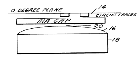
As shown in Figure 6 immediately after printing
the circuit trace on the substrate, the resulting circuit
traces 14 on the circuit board are placed trace side down
to the face 16 of the magnet 18. The preferred distance
from the highest point on the printed circuit trace to the
magnet face is 0.008 inch and this is measured from the
center 20 of the magnet face 16. This is particularly
important when the magnet employed has a spherically formed
face so as to insure correct field strength across the
circuit trace. Dwell time, or exposure of the circuit
trace to the magnetic field can vary depending on the
viscosity of the resin matrix or binder. However, it has
been found that using a resin having a viscosity of 20,000
centipoises, a dwell or exposure period of 3 seconds is
sufficient to compact the magnetite spheres at the upper
level thereof in such a way to increase the conductivity
thereof to the desired levels.
The next step is to expose the circuit board to
a UV source of 380 nm for a period of 8 seconds. While it
is possible to cure the resin in as short a period as 3
seconds, it is imperative that complete polymerization
1335190
throughout the ink film thickness is achieved. In some
situations it may be desirable to irradiate the circuit
board from both the top and bottom thereof due to the
actual protrusion of the spheres through the ink film
thickness. This not only ensures complete polymerization
but it also causes some of the resin to shrink away from
the highest point of the spheres, thus enhancing the
solderability of the trace.
In a preferred embodiment of this second system
a samarium cobalt magnet 18 is employed which has the
following properties:
Peak Energy Density - (BdHd)~x X 10 = 24.0
Residual Induction - Gauss 10,200
Coercive Force - Oersteds 9,200
Saturation Magnetizing Force - Oersteds > 20,000
Where larger circuits are to be exposed to
magnetic levitation it is preferred to use a samarian
cobalt due to its greater peak energy density which is in
the range of from about 20.0 to 28Ø It is important that
when the magnet face is ground with abrasive wheels or the
like that liberal amounts of coolant are employed to
minimize heat cracking and chipping which have an adverse
effect on the uniformity of the magnetic field to which the
circuit trace is exposed.
Another embodiment of the magnetic device
employed in the present invention is shown in Figures 7 and
8.
The magnetic field to be used for levitating the
spheres must not be a uniform field. This is the reason
for the polepiece 22 being added versus a curved magnet 18
previously described. In this alternative device, there
must be a strong gradient of the field, in order that the
upward force on one of the induced poles exceed the
downward force on the other, otherwise there will be no
tendency for the spheres to rise in the ink film thickness.
- 45 -
1335190
.
Using this alternate device, it is much easier to
homogenize the flat magnet in order to achieve uniform peak
field density and use the yoke design with a cold roll
steel polepiece to create a certain area of non-uniformity.
This alternate design provides the necessary
field gradient since the levitating field is constructed in
a configuration that provides a uniform value of the
gradient of the vertical magnetic field along one
horizontal direction and passes the material to be
levitated horizontally through it in a direction
perpendicular to the first. Thus, the necessary gradient
is established by supporting the rare-earth magnet above
the path of the circuit while providing a steel polepiece
underneath that path to guide the field lines into the
return part of the magnetic field. This will subject the
spheres to a lifting force as they enter and again as they
leave the region of the magnetic field.
A vertical gradient in the magnetic field
necessarily is accompanied by a horizontal gradient,
however this alternate device minimizes this condition by
configuring the field such that the horizontal gradient is
in the direction of motion of the substrate. There will be
some horizontal displacement of the spheres, but, being
first forward and then backward along the line of travel,
it does not adversely affect the final resolution.
The maximum remanent magnetism of the magnetite
spheres is about 1.5 emu/gm. This compares with the
minimum value of the saturation magnetization of about 81
emu/gm. This means that there will be very little residual
magnetization in the cured conductive trace and will have
no effect on the ability of the cured trace to conduct an
electric current.
In both the first and second systems described
above adhesion of the printed circuit trace or pattern is
governed by the UV-curable ink composition and substrate
interactions.
- 46 -
1335190
Adequate wetting by close contact of the W -
curable ink composition with the substrate is essential for
the attainment of satisfactory adhesion. Substrate/ink
composition interactions can be both chemical and physical
in nature. Either ions or covalent bonding between the ink
composition and substrate can evolve powerful adhesion
forces. However, owing to the transient time gap and
relatively low temperature, covalent bonding forces are not
easy to create for photo-polymerizable systems.
Generally speaking, adhesion is not a problem for
the curing on porous substrates such as paper and plastics.
Compared to free-radical polymerization, cationic
photo-polymerization does show some advantages on adhesion:
(i) Ionic bonds between the ink composition and
the substrate are more likely formed.
(ii) After curing, the saturated epoxide system
will have less shrinkage than the polymer cured from
unsaturated compounds. Sometimes these shrinkage stresses
in a high-density cross-linked ink composition are strong
enough to tear the coating off the substrate.
Ink compositions for non-porous substrates, such
as steel and copper, will require the addition of a wetting
agent.
In case adhesion is a problem, post-bake may be
required to anneal the film while cooling, thereby relaxing
the residual cure stress.
The present invention also relates to a
composition for use in shielding enclosures housing
electronic equipment and to the enclosure provided with
this shielding composition.
Prior to 1975 most enclosures for business
machines were constructed of metallic materials, such as
die cast zinc or aluminum or sheet metal aluminum or steel.
In the mid-1970's plastics processors developed as a
potential challenger to the metal enclosures, a structural
foam moulded cabinet using some of the newer engineering
- 47 -
1335190
resins. The structural foam process was developed by Union
Carbide in the 1960's and by the mid-1970's the technology
had been developed to the point where foamed units could
offer comparable strength and lighter weight to cold rolled
steel. By the early 1980's the continued miniaturization
of electronic components reduced many of the enclosures to
a size where straight injection moulded units could be used
instead of metal or structural foam.
Further, the conversion from metal to plastic
enclosures is of direct concern to the EPA because it is
certain to increase the incidence of emissions of volatile
organic compounds (VOC's) into the environment from the
surface coatings of these plastic parts. Metal enclosures
are coated either to improve their appearance or to protect
them from environmental stresses. The coatings normally
used on metal cabinets and cases are not high in solids or
VOC's. Plastic parts, on the other hand, are coated for
three major reasons:
a) to improve their appearance;
b) to protect the plastic part from physical and
chemical stress; and
c) to attenuate EMI/RFI.
Because of the nature of plastic and the
different requirements of conventional coatings to ensure
long-term adhesion to the plastic substrate, these surface
coatings are high in solids in an organic solvent
formulation. It can be assumed that the level of VOC
emissions will increase as the conversion from metal to
plastic proceeds and as electronic equipment manufacturers
specify an ever growing amount of surface coatings for
decorative and more importantly EMI/RFI attenuation
purposes.
The major problem observed by the shift from
metal enclosures is the absence of inherent EMI/RFI and ESD
capabilities. Where cold rolled steel or die cast zinc was
used for an enclosure these metals provided the
- 48 -
1335190
conductivity to deal with EMI entering or exiting the
enclosure. Only the apertures where emissions could leak
in or out (e.g. seams, air vents, cable entry points etc.)
had to be shielded for EMI. In the case of non-conductive
plastics, every square inch of surface as well as the
apertures, have to be shielded for EMI, as well as treated
for ESD.
To overcome the disadvantages associated with the
use of a plastic enclosure for electronic equipment the
inventor has discovered that the composition of the present
invention, i.e. a W -curable composition comprising a
suspension of silver-coated magnetic particles in a
cycloaliphatic epoxy resin binder and a cationic photo-
initiator provides an effective shield against EMI
(electromagnetic interference), RFI (radio frequency
interference) or ESD (electrostatic discharge).
While the term "EMI shielding" may be somewhat
loosely employed in the plastics and electronics industry,
nonetheless, the following is an explanation of what this
term means in this field.
There is both natural and man-made
electromagnetic radiation (EMR), and any man-made piece of
digital electronic equipment with a clock emits in
operation an amount of electromagnetic energy; the faster
the clock setting, the greater the amount of energy
emitted. Digital devices utilizing small integrated
circuits and microprocessors can generate a significant
amount of EMR. This EMR can travel out to come into
contact with the conductors of another digital device such
as the power cable, printed circuit boards, and various
connecting wires within the device. The EMR generates a
current independent of the operating current by inducing
current flow in the conductors. A circuit board will
receive and respond to this current just as if it were
receiving the regular operating current. In other words,
this random signal is giving extraneous electrical
- 49 -
1335190
"instructions" to the device that can cause unwantedprogram or data changes. In this example EMR becomes EMI.
10 KHz is the lower boundary for regulations
enforced by the FCC. The problem of emission of and
susceptibility to EMR in this frequency range is referred
to as radio frequency interference (RFI). This is the
range that United States and international regulatory
agencies such as the FCC and VDE are concerned with and is
the range that the composition of the present invention has
been found to control.
Static is a natural phenomenon where a rapid flow
of electrons moves from an electrically charged object to
another object to equalize the potential difference between
them. The rapid flow of electrons can also induce current
flow in conductors by creating EMR. For example, under low
humidity conditions a person walking across a room can act
as a capacitor and build up a charge potential of 10,000
volts or more. This phenomenon is known as electrostatic
discharge (ESD).
Any piece of electrical or electronic equipment
when put into operation generates electromagnetic waves
composed of electrical (E vector) and magnetic (H vector)
impulses. The magnetic impulses can penetrate all plastic
and metal materials except ferrous materials. But magnetic
signals terminate fairly rapidly over a short distance.
Electric fields, on the other hand, can penetrate plastics,
but not grounded metals. These signals can travel much
greater distances. Thus, in electromagnetic energy the
electrical field is the more potent and potentially more
disruptive force.
Computing devices generate timing signals and
pulses at rates of over one million pulses per second in
order to carry out control and logic functions quickly and
efficiently. This electromagnetic and radio frequency
energy is radiated into space and conducted as well through
media such as power lines. This energy has the potential
- 50 -
133Sl9O
to interfere with all forms of conventional electrical and
electronic-radio, telephone and television reception.
The most common form of ESD can generate EMI,
such as walking across a carpet and touching an object like
an electronic device. The conductivity required of the
receptor to protect against ESD is not as great as that
required against EMI from a computing device. So that even
a plastic enclosure which is inherently insulative can
protect against some mild forms of ESD. But nevertheless,
charges can build up in plastic and they will remain there
until sufficient charge is accumulated to be discharged to
a grounded susceptor. If the unit is not properly
grounded, a sufficient charge may build up and the
cumulative electron flow can arc to the circuitry and cause
an EMI problem.
To achieve electromagnetic compatibility (not
generating nor being susceptible to EMI, RFI, or ESD) an
electronic unit has to be designed in such a way to
minimize these emissions or susceptibility. The enclosure
also has to be conducted in such a way as to trap any
residual inward or outward EMI emissions.
The control of electromagnetic interference
involves essentially a shield to contain or envelop the
signals. When an electromagnetic wave encounters a shield,
it will be reflected back to some extent if the impedance
of the wave and that of the shield differ significantly.
Highly conductive metals have a low impedance and they
serve to reflect back the electromagnetic wave. In
contrast, a low impedance magnetic wave encountering metal
with a close match in impedance will result in a transfer
of energy through the metal. Magnetic waves can be very
difficult to shield. Over greater distances the electric
field component dominates, and it is this factor which has
to be dealt with through EMI/RFI shielding.
Electromagnetic waves pass through space or
through non-conductive solid materials at 3 x 10⁸ m/sec.
1335190
When shielding on a non-conductive material, such as most
plastics, is employed, these waves strike the shield and
some of their energy is reflected back just as light
reflects off a mirror. The rest of the energy may be
absorbed in the shield, further attenuating the waves
strength. Technically, there may be a further loss of the
fields strength when the residual energy reaches the
external perimeter of the shielding.
It is an important point to note that in the
context of comparing the various shielding methods to the
shielding composition of the present invention, the
relative thickness of the shielding material has little
effect on the reflected element of the wave, but it has a
strong effect on its absorption. At higher frequencies
reflection decreases and absorption increases. So the
greater attenuation of thicker barriers is important when
dealing with higher frequency outputs.
It is also important to note at this stage that
the absorption effect of an EMI shield will differ
depending on whether the shielding material is entirely or
partly conductive. This is an important distinction
concerning the comparison of the shielding effectiveness of
solid metal surfaces (e.g. zinc arc spray) and metal-filled
coatings (e.g. nickel-based acrylic binders) and the
composition of the present invention.
In summary, electromagnetic energy is an energy
field radiating from an electrical or electronic source
containing both electric and magnetic field components.
The field surrounding a highly electrically charged object
is an electric field. Its presence is manifested by
opposite charge objects clinging together or like charged
objects separating. The field surrounding a highly
magnetically charged object is a magnetic field. Its
presence is manifested by the attraction of other magnetic
materials in the same way that iron filings cling to a
magnet.
- 52 -
1335190
In each case the electric and the magnetic fields
are static; their intensity is constant and there is no
change in either their strength or their position.
However, this can cause arcing. This arcing or
electrostatic discharge (ESD) is a serious problem in
switching electrical circuits since the separation of the
switch or circuit breaker establishes an arc which must be
extinguished in order to break the circuit. Static
discharge can also cause problems through temporary delays
in the transmission of signals.
While metal cabinets or enclosures provide
effective protection against the build-up of static due to
their natural conductivity, plastics will not. Effective
dissipation of ESD is dependent on the placement of the
electronic components within the cabinet and other design
considerations. However, in the area of EMI shielding
which is potentially far more serious, the solutions have
tended to center around providing a metallic coating or
infrastructure to the non-conductive plastic to reduce the
ESD to a minimum.
The static nature of ESD leads to relatively
straightforward solutions to the problem; the level of
shielding required to eliminate ESD is generally fairly
low. Electromagnetic fields, on the other hand, are not
static; their intensity varies and their polarity
alternates. The rate at which the field alternates is the
frequency, measured in cycles per second or Hertz; this
applies to both the electric and the magnetic field
components.
The effectiveness of an EMI shield, as measured
by dB, is referred to as attenuation. Each 10 dB increment
of attenuation or dissipation of energy provides a 10 fold
improvement in shielding effectiveness. A 10 dB
attenuation results in a 90% attenuation of the force
field; 20 dB yields a 99% reduction; 30 dB yields a 99.9%
reduction and so on. In the area of computing devices
- 1335190
generally EMI shielding in the range of from about 1 to
1000 MHz with an attenuation of from about 30 to 40 dB is
sufficient to comply with government regulations in 95% of
all existing business machine applications.
For electric fields reflection is very large
relative to absorption and it occurs primarily on the
surface of the part. This is why thin shields, such as
those obtained by electroless plating, vacuum deposition,
and other thin film metal deposition technologies are very
effective in attenuating electric fields. Conversely, the
primary reflection of magnetic fields is re-reflection
within the shield. Thus, the attenuation of magnetic
fields is best accomplished through thick skin shields,
such as those produced by conductive coatings and zinc arc
spray, and by high magnetic permeability of the shield
material. An important point is that prior to the
development of the shielding material of the present
invention there was no one "perfect" shielding material.
Unique to the shielding material of the present invention
is the high conductivity of the silver coating and the high
magnetic permeability of the magnetite spheres.
The proliferation of EMI and the response to this
growth by various regulatory agencies is attributable to
three basic forces. First, it is due to the tremendous
growth of electronics as an enhancement to productivity in
every aspect of modern life. Secondly, the typical piece
of electronic equipment is more powerful - in other words,
the clocks are working at a faster pace to input and output
the data. Thirdly, there has been a very significant
conversion from metal to plastic enclosures for this
equipment. And, whereas most metals offer a high level of
inherent conductivity, plastics are insulative in nature,
so they are transparent to EMI.
While there has been significant activity in the
development of inherently conductive plastics, nonetheless,
those developed thus far while exhibiting modest amounts of
- 54 -
- 1335190
conductivity, suffer from, inter alia, the following
disadvantages:
a) the materials are only available in sheet
form; and
b) they are highly sensitive to moisture and
air.
Hence, at this time, one principal way to render
a plastic material conductive is to metallize it - either
by the incorporation of metal fillers into a plastic
compound or by surface treatment using pure metal or metal
based coating. While plastics may have replaced metals in
the structure of the enclosures, they still have to rely on
the metals in a plastic/metal marriage to provide all the
properties required of an enclosure that will comply with
EMI/RFI regulations.
As can be seen from the data in the table below,
the shielding composition of the present invention exhibits
significant advantages as an RFI and EMI absorber.
Metal Relative Relative
Conductivitya Permeabilitya
20 Silver 1.05
Iron 0.17 1,000
Relative to copper
Further, the shielding material of the present
invention contains no volatile organic compounds (VOC's),
and it has been demonstrated that a two mil coating of the
shielding composition of the present invention provides the
same shielding effectiveness as a three mil coating of zinc
arc spray or three mils of nickel acrylic coating. This
range is in the neighbourhood of 40-60 dB.
- 55 -